RF Modules
Products (20)

ADAR4002 - 0.5-19GHz Bidirectional TDU | Analog Devices
The ADAR4002 is a low power, broadband, bidirectional, single-channel IC designed for applications requiring programmable time delay and/or attenuation. It operates from 0.5 GHz to 19 GHz, with both RF1 and RF2 ports internally matched to 50 Ω. The device integrates a true time delay unit (TDU) and a digital step attenuator (DSA) in a single package, providing flexible digital control via SPI or shift register interface. The ADAR4002 is available in a 14-lead WFDFN exposed pad package (ACPZ), making it suitable for compact RF front-end designs. A true time delay unit (TDU) is a component that introduces a controlled delay to an RF signal, independent of frequency, which is essential for phased array beamforming and time-domain applications. Unlike phase shifters that only adjust phase, a TDU preserves signal integrity across wide bandwidths, making it critical for wideband systems. The ADAR4002 combines TDU and DSA functions, reducing component count and simplifying system design. Key features include a wide operating frequency range of 0.5 GHz to 19 GHz, bidirectional operation, and low power consumption. The device supports both SPI and shift register control, with on-chip memory for 32 TDU and DSA states. The integrated sequencers allow fast bidirectional memory advance via the UPDATE pin, enabling rapid state changes. The 50 Ω matched ports simplify system integration, and the compact 14-lead WFDFN package supports space-constrained designs. Technically, the ADAR4002 uses a combination of switched delay lines and attenuator stages to achieve precise time delay and attenuation. The bidirectional design allows signal flow in either direction, making it versatile for T/R modules. The SPI interface enables daisy chaining of multiple devices, and the shift register mode provides a simple parallel control option. The device operates over a wide temperature range, ensuring reliability in demanding environments. Typical applications include phased array radar, electronic warfare, 5G beamforming, and test and measurement equipment. The wideband operation and bidirectional capability make it ideal for T/R modules in defense and communication systems. The low power consumption is beneficial for portable and battery-operated systems. When designing with the ADAR4002, ensure proper RF layout and decoupling to maintain performance. The exposed pad should be soldered to a ground plane for thermal and electrical performance. The control interface should be configured according to system requirements, and the memory states should be programmed to achieve the desired delay and attenuation values.
ADMV4821-EVAL - 24-29.5GHz 5G Beamformer Eval Board | Analog Devices
The ADMV4821-EVAL is an evaluation board from Analog Devices designed to evaluate the ADMV4821, a silicon germanium (SiGe), 24 GHz to 29.5 GHz, dual-polarization 5G beamformer. The board integrates the ADMV4821 with low dropout (LDO) regulators, level shifters, and an EVAL-SDP-CS1Z (SDP-S) controller board, enabling simplified and efficient evaluation of the beamformer's 16 transmit and 16 receive channels. The ADMV4821 supports the n257, n258, and n261 5G NR bands in a single footprint, with matched 50-ohm single-ended RF inputs and outputs for both horizontal and vertical polarizations. A beamformer is a highly integrated RF front-end component that electronically steers antenna beams by adjusting the phase and amplitude of signals across multiple antenna elements. In massive MIMO systems, beamformers like the ADMV4821 are essential for achieving the high data rates and spectral efficiency required by 5G networks. The ADMV4821 belongs to the class of millimeter-wave (mmW) beamformer ICs, which are part of the broader category of RF front-end modules used in base stations and user equipment. Key features of the ADMV4821 include 16 selectable TX channels and 16 selectable RX channels, dual polarization support, and a frequency range covering 24 GHz to 29.5 GHz. The evaluation board simplifies testing by providing all necessary power regulation and control interfaces, allowing engineers to focus on RF performance validation. The board is designed for use with the SDP-S controller, which provides a USB interface for software control of the beamformer's settings. The ADMV4821 is fabricated in a SiGe process, offering a good balance of performance and integration for mmW applications. The device includes on-chip LDO regulators to ensure clean power delivery to the RF circuitry, reducing external component count. The evaluation board's layout is optimized for 50-ohm impedance matching, ensuring accurate measurements of gain, phase, and beamforming performance. Typical applications for the ADMV4821-EVAL include 5G NR base station development, phased array antenna prototyping, and beamforming algorithm validation. The board is also useful for evaluating the ADMV4821 in test and measurement setups, where its wide frequency coverage and dual-polarization capability are advantageous. When using the ADMV4821-EVAL, ensure proper power sequencing and control via the SDP-S board. The evaluation board requires a 5V supply and a USB connection to the controller. For accurate RF measurements, use calibrated test equipment and follow the guidelines in the user guide UG-1564.
ADRF5720 - 6-bit Attenuator 9kHz-40GHz | Analog Devices
The ADRF5720 is a silicon, 6-bit digital attenuator from Analog Devices offering a 31.5 dB attenuation control range in 0.5 dB steps. It operates from 9 kHz to 40 GHz with better than 4.5 dB of insertion loss and excellent attenuation accuracy. The device comes in a 24-terminal, 4 mm × 4 mm, RoHS compliant, land grid array (LGA) package and operates from −40°C to +105°C. The RF ports are designed to match a characteristic impedance of 50 Ω. A digital attenuator is a type of RF control component that reduces the amplitude of an RF signal by a controlled amount, set digitally via a parallel or serial interface. It belongs to the broader family of RF signal-conditioning components that includes switches, phase shifters, and variable gain amplifiers. Digital attenuators are essential in applications such as automatic gain control (AGC), signal leveling, calibration, and gain compensation in communication, radar, and test-and-measurement systems. Key features of the ADRF5720 include its ultra-wideband frequency coverage from 9 kHz to 40 GHz, which is rare among digital attenuators, and its high attenuation accuracy. The device is pin-compatible with the ADRF5730, the fast switching version that operates from 100 MHz to 40 GHz. This allows designers to upgrade or downgrade between the two parts without PCB changes. The ADRF5720 also features a serial interface for setting attenuation, and it operates from a single 3.3 V or 5 V supply. The ADRF5720 is fabricated using a silicon process, which provides high linearity and low power consumption. The device includes an on-chip driver and a serial-to-parallel interface, simplifying integration into digital control systems. The LGA package is designed for high-frequency performance, with low parasitic inductance and capacitance. The exposed pad provides a low thermal resistance path, enabling efficient heat dissipation at up to 500 mW RF power handling. Typical applications for the ADRF5720 include AGC loops, signal leveling in test equipment, radar calibration, gain compensation in communication systems, and power control in satellite ground terminals. Its wide frequency range makes it suitable for both low-frequency baseband and high-frequency microwave applications up to 40 GHz, including 5G mmWave bands. The device is also commonly used in RF front-end protection and broadband transceiver power leveling. When designing with the ADRF5720, it is important to provide adequate grounding and decoupling. The RF input and output ports should be matched to 50 Ω, and the control lines should be properly terminated to avoid spurious responses. The device's serial interface should be programmed according to the datasheet timing requirements to ensure accurate attenuation settings.
ESP32-C5-WROOM-1 - Dual-Band Wi-Fi 6 BLE Zigbee Module | Espressif
The Espressif ESP32-C5-WROOM-1 is a general-purpose 2.4 and 5 GHz dual-band Wi-Fi 6 (802.11ax) module with Bluetooth 5 (LE), Zigbee, and Thread (IEEE 802.15.4) connectivity, built on a single-core RISC-V MCU clocked up to 240 MHz, housed in a 27.5 x 18 mm surface-mount castellated-pad module with a PCB trace antenna. A wireless module is a pre-certified, fully integrated subassembly that combines a microcontroller SoC, RF front end, antenna, crystal, and flash memory on one small PCB, so designers add connectivity to a product without designing a radio from scratch. In the system hierarchy, a module sits above the SoC level (SoC -> module -> development board) and below complete end products, drastically shortening time-to-market for IoT devices and reducing RF certification effort. Key features include industry-first 5 GHz dual-band Wi-Fi 6 support in a RISC-V MCU, multi-protocol operation spanning 802.11ax, Bluetooth 5 LE, Zigbee, and Thread, and flash options ranging from 4 MB to 32 MB QuadSPI depending on the ordering code. The dual-band capability lets products use the less congested 5 GHz band for higher throughput and lower interference, a decisive advantage in dense smart-home deployments. Technically, the module is built around the ESP32-C5 SoC, which Espressif describes as the industry's first RISC-V MCU supporting 2.4/5 GHz dual-band Wi-Fi 6 alongside IEEE 802.15.4. This allows Matter-over-Thread and Zigbee 3.0 devices to coexist with Wi-Fi on a single chip, simplifying border-router and hub architectures. The ambient operating temperature range is -40 to +85 C per the module datasheet family table. Typical applications include smart-home devices (Matter, Thread, Zigbee), industrial automation nodes, healthcare and consumer electronics, where the rich peripheral set and multi-protocol radio reduce external component count. For design-in, note that strapping pins and the antenna keep-out area must follow Espressif's hardware design guidelines; the module requires a clean 3.3 V supply with adequate peak current capability for Wi-Fi 6 TX bursts. This page synthesizes datasheet specifications, family variants, drop-in alternatives, and practical design guidance not consolidated in the manufacturer datasheet alone.
ESP32-C5-WROOM-1U-N8R8 - Dual-Band Wi-Fi 6 BLE Module | Espressif
The Espressif Systems ESP32-C5-WROOM-1U-N8R8 is a general-purpose 2.4 GHz and 5 GHz dual-band Wi-Fi 6 (802.11ax) module with Bluetooth 5 (LE), Zigbee, and Thread (802.15.4) connectivity, built around a 32-bit RISC-V single-core processor running at up to 240 MHz, with 8 MB Quad SPI flash and 8 MB Quad SPI PSRAM in an 18.0 x 21.2 x 3.3 mm surface-mount package with an IPEX (U.FL) connector for an external antenna. A wireless module is a pre-certified, self-contained circuit board that integrates a microcontroller SoC, RF front end, crystal, flash memory, and antenna interface into a single castellated-edge surface-mount unit. Modules sit above bare SoCs in the electronics hierarchy - embedded system, wireless connectivity module, SoC, silicon - and let designers add certified radio connectivity without in-house RF design or regulatory re-certification. Key features include simultaneous dual-band Wi-Fi 6 support in the 2.412-2.484 GHz and 5.18-5.885 GHz bands, which reduces congestion in dense IoT deployments; 802.15.4 radio for Zigbee and Thread, enabling native Matter and Thread mesh networks; Bluetooth 5 LE for phone provisioning and beacons; and a low-power coprocessor that can monitor peripherals while the main CPU is powered off. At the core is the ESP32-C5 SoC, a single-core 32-bit RISC-V processor clocked up to 240 MHz with a rich peripheral set including SPI, I2C, UART, I2S, PWM, and ADC. The N8R8 variant pairs 8 MB flash with 8 MB PSRAM, providing ample headroom for TLS stacks, display buffers, and Matter applications. Typical applications include smart home hubs that must bridge Wi-Fi, Thread, Zigbee, and BLE simultaneously; industrial automation gateways using the 5 GHz band to avoid 2.4 GHz factory interference; and healthcare or consumer electronics requiring dual-stack wireless provisioning. For design, keep the IPEX antenna feedline at 50 ohms impedance and follow Espressif hardware design guidelines for module keep-out zones. Note that the 1U variant has no onboard PCB antenna, so an external antenna is mandatory. This page synthesizes verified datasheet specifications, drop-in same-family alternatives, and practical design notes not found on distributor listing pages.
ESP32-WROOM-32E - WiFi + BT 4.2 MCU Module | Espressif
The Espressif Systems ESP32-WROOM-32E is a 2.4 GHz Wi-Fi and Bluetooth/Bluetooth LE combination module built around the ESP32-D0WD-V3 dual-core Xtensa LX6 SoC, delivering up to 240 MHz clock speed, 520 KB SRAM, and 4 MB SPI flash in a compact 18 x 25.5 x 3.1 mm castellated-pad module with an integrated PCB antenna. A Wi-Fi + Bluetooth MCU module is a surface-mount system-in-package that combines a microcontroller, radio transceiver, RF matching network, flash memory, crystal, and antenna onto a single certified PCB assembly. Such modules sit at the top of the embedded hierarchy: semiconductor -> wireless SoC -> RF-certified module -> end IoT device, letting engineers add wireless connectivity without RF design expertise or regulatory re-certification of the radio section. Key differentiating features include dual-core processing that separates Wi-Fi protocol stacks from user applications, 802.11 b/g/n with a data rate up to 150 Mbps, Bluetooth v4.2 BR/EDR and BLE Class 1/2/3 operation, and 38 castellated edge pads that allow both hand soldering and automated assembly. The castellated half-hole pads also enable mounting the module as a sub-PCB on a carrier board. Technically, the ESP32-D0WD-V3 silicon inside is the bug-fixed revision 3 die, improving RF transmit spectrum cleanliness and resolving the well-known strapping-pin flash-voltage issue found in older revision 1 silicon used in the original ESP32-WROOM-32. The module integrates a 40 MHz crystal, flash memory, and a PCB inverted-F antenna tuned during production. Typical applications include low-power sensor networks, voice encoding and MP3 streaming devices, smart-home nodes, and industrial IoT gateways, where integrated dual-radio connectivity and sufficient compute headroom are required in one certified package. For design, respect the strapping pins (GPIO0, GPIO2, GPIO12, GPIO15) at boot and keep the antenna area of the host PCB free of copper and components for best RF performance. This page synthesizes datasheet specifications, drop-in replacement options, and practical design notes not found on standard distributor listings.
ESP32-WROOM-32E-H4 - WiFi BT4.2 Module 4MB | Espressif
The Espressif Systems ESP32-WROOM-32E-H4 is a 2.4 GHz WiFi and Bluetooth 4.2 +BR/EDR/BLE combination module built on the ESP32-D0WD-V3 dual-core Xtensa LX6 SoC with 4 MB of embedded SPI flash, a PCB antenna, and a 25.5 x 18 x 3.1 mm castellated SMD package rated from -40C to +105C. A WiFi module is a self-contained embedded system that integrates a microcontroller, radio transceiver, antenna, flash memory, and power management into a single surface-mount unit, eliminating the RF design effort of discrete solutions. Within the wireless connectivity hierarchy, the ESP32-WROOM-32E-H4 sits at the system-in-package (SiP) module level: SoC (ESP32-D0WD-V3) -> module (WROOM-32E family) -> IoT device. Modules are pre-certified for radio regulatory domains, shortening time to certification for end products. Key features include dual-core 32-bit LX6 CPUs clocked up to 240 MHz, 520 KB on-chip SRAM, 802.11 b/g/n WiFi with up to 150 Mbps PHY rate and -98 dBm receive sensitivity, Bluetooth v4.2 BR/EDR and BLE, and 26 GPIOs with UART, SPI, I2C, SDIO, I2S, PWM, and 12-bit ADC peripherals. The -H4 suffix denotes 4 MB SPI flash; supply range is 3.0 V to 3.6 V with typical TX current around 112 mA and peak around 239 mA at 20 dBm output. The ESP32-D0WD-V3 silicon (ECO V3) incorporates the bug fixes and cleaner WiFi RF spectrum of the revised ESP32 revision, improving coexistence and reliability compared with original ESP32-WROOM-32 modules. The onboard PCB antenna is tuned for 2.4 GHz to 2.5 GHz operation, and the metal shield plus castellated edge pads simplify reflow assembly onto standard PCB footprints. Typical applications include smart-home devices and sensors, industrial automation and control nodes, and battery-powered IoT endpoints where integrated dual-protocol wireless reduces BOM cost and development risk. A key design consideration: the module is 3.3 V only - do not feed 5 V logic into GPIOs without level shifting, and keep copper keep-out clearance under and around the PCB antenna per Espressif hardware design guidelines. This page adds value beyond the datasheet by synthesizing distributor pricing tiers, drop-in same-footprint alternatives across flash densities, and practical engineering design notes in one place.
ESP32-WROOM-32E-N8 - WiFi/BT4.2 Module, 8MB Flash | Espressif
The Espressif Systems ESP32-WROOM-32E-N8 is a 2.4 GHz Wi-Fi and Bluetooth 4.2 + EDR combo module built on the ESP32-D0WD-V3 SoC with a dual-core 32-bit Xtensa LX6 processor running up to 240 MHz, 8 MB of SPI flash, and an onboard PCB antenna, housed in a 38-pin surface-mount castellated package measuring 18 x 25.5 x 3.1 mm. A Wi-Fi/BT module is an RF transceiver subsystem that integrates the radio, antenna, crystal, flash memory, and power management into a certified, ready-to-embed unit. Within the wireless connectivity hierarchy, it sits above bare SoCs (which require external RF design) and below finished development boards, serving as the standard connectivity building block for IoT products. Key features include 802.11 b/g/n Wi-Fi with Class 1, 2 and 3 Bluetooth transmit capability, 26 usable GPIOs, a rich peripheral set (SPI, I2C, UART, I2S, CAN, touch sensors, ADC/DAC), and support for simultaneous Wi-Fi and Bluetooth operation. The 8 MB SPI flash supports large application images, OTA updates, and embedded assets. Technically, the module integrates the ESP32-D0WD-V3 silicon revision 3 chip, which fixes earlier RF spectral spur issues for a cleaner Wi-Fi spectrum. The ESP32-WROOM-32E family offers 4/8/16 MB flash options; the -N8 variant is the 8 MB member. The PCB antenna is tuned for the 2.400-2.4835 GHz ISM band. Typical applications include IoT sensor nodes and smart-home devices, industrial wireless control and monitoring, and wearable or battery-powered connected products. Design consideration: keep at least 5 mm of clearance around the PCB antenna region on the host board and follow the Espressif layout guidelines to avoid detuning RF performance; supply 3.0-3.6 V with adequate peak-current capability for Wi-Fi TX bursts. This page synthesizes distributor pricing, drop-in alternatives within the same footprint, and practical design notes not found in the manufacturer datasheet.
ESP32-WROOM-32E-N8R2 - WiFi/BT 4.2 Module, 8MB Flash | Espressif
The Espressif Systems ESP32-WROOM-32E-N8R2 is a 2.4 GHz Wi-Fi and Bluetooth v4.2 + EDR combo module built around the ESP32-D0WD-V3 SoC with Xtensa dual-core 32-bit LX6 processors, 8 MB of SPI flash and 2 MB of PSRAM, delivered in a shielded surface-mount package with an onboard PCB trace antenna. A Wi-Fi MCU module is a self-contained wireless system that integrates a microcontroller, radio transceiver, antenna, RF matching network, flash memory and power management on one certified PCB. Within the product hierarchy it sits between a bare SoC and a full development board: it offers complete radio certification and shielding without the overhead of a carrier board, making it the standard building block for power management, connectivity and edge computing in IoT endpoints. Key features of the N8R2 variant include 802.11 b/g/n Wi-Fi with 150 Mbps PHY rate, Bluetooth v4.2 BR/EDR and BLE, dual-core LX6 operation for concurrent application and protocol processing, and 26 GPIOs with a rich peripheral set (SPI, I2S, I2C, UART, ADC, DAC, PWM, touch). The 8 MB flash plus 2 MB PSRAM configuration gives headroom for OTA update partitions, larger TLS stacks and display frame buffers that smaller N4/N8 variants cannot support. Technically, the module integrates antenna switches, RF balun, power amplifier, low-noise receive amplifier, filters and power management on the embedded ESP32-D0WD-V3 silicon, achieving higher stability and safety performance than the original ESP32-WROOM-32. The V3 die revision adds security features such as flash encryption and secure boot support. Typical applications include smart-home devices, industrial controllers and wireless sensor nodes where both Wi-Fi and Bluetooth connectivity and extra RAM are required in a single certified footprint. Design-wise, supply the module from a clean 3.3 V rail capable of delivering 500 mA peaks, and keep the antenna region free of copper and enclosures with high dielectric constants. This page synthesizes distributor pricing, memory-variant drop-in options and practical design notes not found in the manufacturer datasheet. Pricing references are as of 2026-09-15.

HMC649A - 6-Bit Digital Phase Shifter 3-6 GHz | Analog Devices
The HMC649A is a GaAs MMIC 6-bit digital phase shifter designed for operation from 3 GHz to 6 GHz, manufactured by Analog Devices. It provides 64 phase states with a typical RMS phase error of 4 degrees and extremely low insertion loss variation of ±0.5 dB across all phase states. The device is controlled with positive control logic of 0/+5V and is housed in a compact 6x6 mm plastic leadless SMT package (28-QFN). It is internally matched to 50 Ohms, requiring no external components. A digital phase shifter is a critical component in RF and microwave systems that alters the phase of an incoming signal by a discrete amount, controlled by digital bits. It is used in phased array antennas, radar systems, and communication systems to steer beams electronically. The HMC649A belongs to the category of RF phase shifters, which are essential for beamforming and signal conditioning in modern wireless infrastructure. Key features of the HMC649A include 6-bit resolution providing 64 phase states, a frequency range of 3 GHz to 6 GHz, and a typical insertion loss of [DATA_NEEDED: insertion loss] dB. The device operates with a supply voltage of Vdd=+5V and Vss=-5V, and control voltage of 0/+5V. It is recommended for new designs and is available in a 28-QFN (6x6 mm) package, suitable for surface mount assembly. The HMC649A utilizes GaAs MMIC technology, offering high performance and reliability for demanding RF applications. The device's low RMS phase error and consistent insertion loss across all states ensure accurate beamforming and signal integrity. Its compact package and 50 Ohm internal matching simplify PCB design and reduce external component count. Typical applications include phased array radar, satellite communications, and 5G beamforming systems. The HMC649A is also used in test and measurement equipment for phase calibration and in electronic warfare systems for signal manipulation. When designing with the HMC649A, ensure proper power supply decoupling and control logic interfacing. The device requires both positive and negative supply rails, and the control lines should be driven with appropriate logic levels to achieve accurate phase states.
HMC649ALP6E - 6-Bit Digital Phase Shifter 3-6GHz | Analog Devices
The HMC649ALP6E is a GaAs MMIC 6-bit digital phase shifter from Analog Devices, operating from 3 to 6 GHz. It provides 360 degrees of phase coverage with a least significant bit (LSB) of 5.625 degrees, enabling precise phase control for radar and communication systems. The device is housed in a compact 6x6 mm plastic leadless SMT package (28-QFN) and is internally matched to 50 Ohms, requiring no external components. A digital phase shifter is a critical RF component that alters the phase of an incoming signal by discrete steps, controlled by digital logic. It is a subset of phase shifters, which are essential in phased-array antennas, beamforming networks, and radar systems. The HMC649ALP6E belongs to the family of RF/microwave ICs, specifically within the category of phase shifters, which are used to steer antenna beams electronically without moving parts. Key features include extremely low insertion loss variation of ±0.5 dB across all phase states, high accuracy with a phase error of ±4 degrees, and positive control logic of 0/+5V. The device operates over a wide temperature range and is RoHS compliant. Its 6-bit resolution provides 64 distinct phase states, allowing fine-grained beam steering. Technically, the HMC649ALP6E uses GaAs MMIC technology, which offers high electron mobility and low noise, making it suitable for high-frequency applications. The phase shifter is designed for use in radar systems, satellite communications, and test equipment. Its 50-ohm internal matching simplifies integration into RF chains, reducing design complexity and component count. Typical applications include phased-array radar, electronic warfare systems, and 5G beamforming. The device's wide bandwidth and precise phase control make it ideal for these demanding applications. When designing with this component, ensure proper grounding and decoupling to maintain performance. The control logic inputs should be driven with a 0/+5V signal, and the RF input/output should be AC-coupled to prevent DC bias issues.
HMC649ALP6ETR - 6-Bit Digital Phase Shifter 3-6GHz | Analog Devices
The HMC649ALP6ETR is a 6-bit digital phase shifter from Analog Devices, designed for RF applications operating from 3 GHz to 6 GHz. It provides 64 phase states with a 5.625° step, covering 0° to 360° with low insertion loss and high accuracy. The device is housed in a compact 28-lead QFN (6x6 mm) package, making it suitable for space-constrained radar and communication systems. A digital phase shifter is a critical RF component that adjusts the phase of a signal passing through it, controlled by digital logic bits. It is used in phased-array antennas, beamforming networks, and radar systems to steer the antenna beam electronically without moving parts. The HMC649ALP6ETR integrates the phase-shifting network and digital control interface into a single MMIC, simplifying system design and reducing board space. Key features include a frequency range of 3 GHz to 6 GHz, 6-bit resolution with 64 phase states, low insertion loss of typically 6 dB, and RMS phase error of less than 3 degrees. The device operates with a single +5V supply and a -5V supply, with control voltages of 0/+5V. It is fabricated using GaAs MMIC technology, ensuring consistent performance across temperature and process variations. The HMC649ALP6ETR uses a switched-line phase shifter architecture, where different path lengths are selected by PIN diodes or FET switches to achieve precise phase shifts. This design provides wideband performance and high power handling capability. The digital control interface is compatible with TTL/CMOS logic levels, allowing direct connection to microcontrollers or FPGAs. Typical applications include phased-array radar, satellite communications, 5G beamforming, and test equipment. The device's wide frequency range and high phase accuracy make it ideal for both military and commercial systems. Its small package and low power consumption enable integration into portable and handheld devices. When designing with this device, ensure proper decoupling of the Vdd and Vss supplies and provide adequate ground vias under the exposed pad for thermal and electrical performance. The control lines should be kept short to minimize parasitic inductance and maintain fast switching speeds.
QPM1002 - 8.5-10.5GHz GaN X-Band T/R FEM 3W | Qorvo
The Qorvo QPM1002 is a Gallium Nitride (GaN) MMIC front-end module (FEM) for X-Band radar applications covering 8.5 GHz to 10.5 GHz, integrating a T/R switch, a low-noise amplifier, and a power amplifier in a 5 x 5 mm QFN surface-mount package with over-mold encapsulant. A front-end module (FEM) is a highly integrated RF building block that sits between the antenna and the transceiver in a radar system. In an X-Band phased array radar, the FEM performs three critical functions: amplifying weak received echoes (LNA path), amplifying transmitted pulses (PA path), and switching between the two (T/R switch). Integrating all three on a single GaN-on-SiC die reduces board area, assembly variation, and lattice-spacing constraints compared to discrete multi-chip solutions. According to the Qorvo datasheet, the receive path delivers 25 dB of small-signal gain with a low noise figure of 2.2 dB, maximizing radar detection range against small targets. The transmit path provides 33 dB of small-signal gain and can deliver 3 W of saturated output power with a power-added efficiency (PAE) of 32%. The ANT port tolerates up to 2 W of input power, eliminating the need for an external limiter diode and its associated insertion loss. The module is fabricated on Qorvo's QGaN25 0.25 um GaN-on-SiC process. The high thermal conductivity die-attach, combined with the over-molded QFN package, allows reliable operation in high-temperature environments typical of airborne and ground-based phased array antennas. Typical applications include X-Band phased array radar transmit/receive (T/R) channels, marine and weather radar, and airborne surveillance systems where compact size and high power density are mandatory. Design consideration: the high power density of GaN requires a well-designed thermal path; the exposed package paddle must be soldered to a low-thermal-resistance via array in the PCB. This page synthesizes distributor sourcing data, drop-in alternative guidance, and practical design notes not found in the manufacturer datasheet.
QPM1002SR - X-Band 3W GaN T/R FEM 8.5-10.5GHz | Qorvo
The Qorvo QPM1002SR is an 8.5-10.5 GHz GaN MMIC front-end module (FEM) integrating a T/R switch, low-noise amplifier, and power amplifier in a 5 x 5 mm over-molded QFN surface-mount package. The receive path provides 25 dB of gain with a 2.2 dB noise figure, while the transmit path delivers 33 dB small-signal gain, 3 W of saturated output power, and 32% power-added efficiency (PAE). A transmit/receive module is a bidirectional RF front end that shares a single antenna between a transmitter and a receiver using a T/R switch. In the system hierarchy, it sits above individual MMIC amplifiers, combining switching, LNA, and PA functions into one module, and is a core building block of power management for radar front ends. Modules like the QPM1002 reduce component count, footprint, and assembly tolerance compared to discrete chains. Key differentiating features include the integration of three functions (switch, LNA, PA) on a single die-level module, which minimizes interconnect losses and lattice pitch. According to Qorvo, the part is fabricated on the QGaN25 0.25 um GaN-on-SiC process, whose wide bandgap supports high power density and ruggedness. The over-mold encapsulant combined with a proprietary high-thermal-conductivity die-attach allows operation in elevated-temperature environments, and the compact 5 x 5 mm footprint supports the tight lattice spacing required by X-Band phased array radar. Technically, the GaN-on-SiC construction offers superior thermal conductivity relative to GaAs, enabling higher channel temperatures to be tolerated and higher power density per millimeter of gate periphery. The 0.25 um gate length of the QGaN25 process supports X-Band frequencies with good efficiency, and the integrated T/R switch eliminates the insertion loss of an off-module circulator or switch in compact arrays. Typical applications include X-Band phased array radar transmit/receive channels, military and commercial radar front ends, and airborne or ground-based surveillance radar systems. In phased arrays, the module's small size directly determines achievable element pitch at 8.5-10.5 GHz. When designing with this module, thermal management is the primary consideration: the GaN die dissipates substantial heat at 3 W RF output, so the PCB ground vias and heat-spreading copper must be designed for the high-thermal-conductivity die-attach to work as intended. Bias sequencing and switch control timing should follow the manufacturer datasheet. This page synthesizes distributor availability, verified datasheet parameters, and practical design guidance for the QPM1002SR not consolidated in the manufacturer datasheet.
RS9116N-DB00-CC1-B2A - Dual-Band Wi-Fi + BT5 Module | Silicon Labs
The Silicon Labs RS9116N-DB00-CC1-B2A is a dual-band (2.4 GHz and 5 GHz) multi-protocol wireless connectivity module delivering 802.11 a/b/g/n Wi-Fi and dual-mode Bluetooth 5 in a surface-mount castellated CC1 module package with no external antenna included. A wireless connectivity module is a self-contained RF subsystem that integrates the radio transceiver, RF front end, crystal, and regulatory-certified antenna matching network into one certified unit. Modules sit above discrete SoCs in the system hierarchy (module -> RF subsystem -> connectivity IC -> wireless SoC) because they shorten time to market: the RF design is pre-validated, and FCC, IC, and ETSI/CE certifications carry over to the host product, eliminating costly in-house regulatory testing. Key features include simultaneous 2.4 GHz and 5 GHz band support for 802.11n clients and access points, dual-mode Bluetooth 5 for classic and low-energy links, and host interfacing over SDIO or USB. The module is FCC, IC, and ETSI/CE certified, and Silicon Labs supplies drivers for Linux and other high-level operating systems. Power-optimized performance extends battery life in portable designs while maintaining extended range. The -B2A suffix denotes the factory-preloaded firmware version, per the ordering information in the RS9116 CC1 datasheet; -B2B variants differ only in firmware. The RS9116N targets n-Link deployments, where the networking stack runs on the host Linux application processor and the module handles the wireless PHY/MAC. Operating modes include Wi-Fi Client, Wi-Fi Access Point, and Simultaneous Client plus Access Point, with up to 50 Mbps Wi-Fi application throughput per Silicon Labs n-Link documentation. Typical applications include industrial gateways and routers, Linux-based embedded systems needing certified dual-band connectivity, medical and instrumentation devices streaming data over Wi-Fi with a Bluetooth 5 provisioning path, and smart-building infrastructure. Design consideration: the module does not include an antenna, so an external antenna with matching 50-ohm feed must be selected and placed per the Silicon Labs layout guidance to preserve certification limits. This page adds value beyond the datasheet by synthesizing distributor availability, drop-in firmware-variant alternatives, cross-brand comparison candidates, and practical design notes in one reference.

RTAX4000SL-CQ352PROTO - 4M-Gate Radiation-Tolerant FPGA | Microchip
The Actel (Microchip/Microsemi) RTAX4000SL-CQ352PROTO is a radiation-tolerant, one-time-programmable FPGA with 4,000,000 equivalent system gates, 60,480 logic cells, and 40,320 CLBs, housed in a 352-pin ceramic CQFP (CQ352) metal-sealed cofired package. The PROTO suffix denotes a prototyping-oriented ordering option within the RTAX-S/SL space-flight family. A radiation-tolerant FPGA is a field-programmable gate array engineered to survive the total ionizing dose (TID), single-event latchup (SEL), and single-event upset (SEU) environment encountered in Earth-orbiting and deep-space missions. Within the power-management hierarchy of spacecraft avionics, such devices occupy the top tier of programmable logic, sitting above commercial FPGAs and below full rad-hard ASICs in cost and flexibility. Key differentiating features include true single-chip form factor enabled by antifuse programmability, live-at-power-up operation with no configuration device required, low static power consumption, and embedded SRAM blocks with built-in FIFO control logic. The RTAX-S/SL architecture derives from the commercial Microsemi Axcelerator family, inheriting segmentable clocks, chip-wide highway routing, and dedicated carry logic for arithmetic. Architecturally, each cluster contains logic cells built around register-rich C-cells and R-cells, with a maximum CLB combinatorial delay of 1.1 ns per the Microchip USA product listing. The CMOS process, combined with the ceramic metal-sealed CQFP352 package, supports operation across a military/space temperature range of -55C to +125C in surface-mount assembly. Typical applications include satellite payload data processing, spacecraft bus command and data handling, telecommunication transponder control, and launch-vehicle avionics, where single-chip integration and SEU robustness are decisive. A key design consideration is that antifuse RTAX devices are one-time programmable: engineers typically validate logic on an Aldec flash-based prototyping adaptor (e.g., ACT-H3Ki-CQ352) before committing to flight silicon, which is precisely the role the PROTO ordering option targets. This page synthesizes distributor listings, drop-in alternatives, and practical design notes not found in the manufacturer datasheet.
RUBY-W2 - Automotive Tri-Band Wi-Fi 7 + BT 5.4 Module | u-blox
The u-blox RUBY-W2 is an automotive-grade, host-based wireless module featuring tri-band Wi-Fi 7 (802.11be) and Bluetooth 5.4 Dual-Mode (BR/EDR + LE), engineered for high-reliability in-vehicle infotainment (IVI) and telematics applications requiring high throughput, such as in-car hotspots, smartphone display integration (Apple CarPlay), and multi-client video streaming. A host-based wireless module is a communication component that offloads the Wi-Fi/Bluetooth protocol stack to a companion application processor rather than running it on-chip. In the system hierarchy, it sits below the vehicle's infotainment SoC within the connectivity layer of the automotive electronics architecture, connecting to host processors running Linux or Android through standard host interfaces. Key features include Wi-Fi 7 Multi-Link Operation (MLO) with Dual Band Simultaneous (DBS) capability, which raises throughput, supports more concurrent clients, and reduces latency versus prior Wi-Fi generations. Bluetooth 5.4 dual-mode support covers high data rates, extended advertising, long-range (coded PHY), and isochronous channels for LE Audio, operating fully simultaneously with Wi-Fi. Automotive qualification targets the harsh reliability and quality requirements of in-vehicle deployments, including extended temperature operation and rigorous testing per u-blox automotive workflows. The RUBY-W2 family includes variants such as the RUBY-W272 and RUBY-W273, which implement Dual Band Simultaneous Wi-Fi 7 operation. Host processors communicate with the module over its supported high-speed interfaces, allowing OEMs to keep the wireless stack and driver software on the IVI host and update connectivity features over the vehicle lifecycle. According to u-blox product documentation, the modules are designed, built, and tested specifically for advanced infotainment and telematics use cases. Typical applications include in-car Wi-Fi hotspots serving multiple passengers, wireless Apple CarPlay and Android Auto projection displays, rear-seat video streaming, telematics control units with high-bandwidth uplink assist, and OTA software update distribution over Wi-Fi 7 links. A key design consideration is that this is a host-based module: the designer must allocate host CPU resources and memory for the wireless stack and validate RF coexistence and antenna integration within the vehicle, rather than treating the module as a fully autonomous connectivity appliance. This page adds value beyond the manufacturer datasheet by consolidating verified sourcing links, same-family drop-in alternatives, application guidance, and practical design notes for automotive wireless integration.
SIM800C - Quad-Band GSM/GPRS Module | SIMCom
The SIM800C is a complete Quad-Band GSM/GPRS module in a compact LCC (Leadless Chip Carrier) package, designed by SIMCom Wireless Solutions. It operates on 850/900/1800/1900 MHz frequencies and supports GPRS data transfer up to 85.6 kbps. The module measures 17.6 x 15.7 x 2.3 mm, making it suitable for space-constrained IoT and embedded applications. It requires a supply voltage of 3.4V to 4.4V and features a 42-pin SMD interface. A GSM/GPRS module is a cellular communication module that enables devices to connect to GSM networks for voice, SMS, and data services. It integrates a baseband processor, RF transceiver, and power management into a single package, allowing developers to add cellular connectivity to their products without designing complex RF circuitry. The SIM800C sits within the hierarchy of cellular modules, which includes 2G, 3G, 4G LTE, and NB-IoT categories, and is specifically a 2G GSM/GPRS module. Key features of the SIM800C include support for Quad-Band frequencies, GPRS multi-slot class 12, and a rich set of interfaces including UART, USB 2.0, GPIO, SPI, and I2C. It also integrates an audio codec with speaker and microphone amplifiers, making it ideal for voice applications. The module supports AT command control, enabling easy integration with microcontrollers. Its low power consumption in sleep mode (around 1 mA) is beneficial for battery-powered devices. Technically, the SIM800C is built on a mature GSM/GPRS platform, offering reliable performance in 2G networks. It supports SMS, voice calls, and data transmission, with a maximum GPRS downlink speed of 85.6 kbps. The module includes a power management unit that handles over-voltage and under-voltage protection, ensuring safe operation. It also features a PWRKEY pin for power-on/off control and supports normal power-off via AT command 'AT+CPOWD=1'. Typical applications include remote monitoring, asset tracking, alarm systems, smart metering, and IoT gateways. Its compact size and low power consumption make it suitable for portable devices, while its robust interface set allows for flexible system integration. The SIM800C is widely used in industrial and consumer applications where 2G connectivity is still available. When designing with the SIM800C, ensure a stable power supply within 3.4V to 4.4V and adequate decoupling. The module requires a proper antenna connection and careful PCB layout to minimize RF interference. Also, consider the lifecycle status, as 2G networks are being phased out in many regions, which may affect long-term deployment.
SIM800C - Quad-Band GSM/GPRS Module | SIMCom | IoT & M2M
The SIM800C is a complete Quad-Band GSM/GPRS module in a compact LCC (Leadless Chip Carrier) package, designed by SIMCom Wireless Solutions. It operates on 850/900/1800/1900 MHz frequencies and supports GPRS data transfer up to 85.6 kbps. The module measures only 17.6 x 15.7 x 2.3 mm, making it ideal for space-constrained IoT and M2M applications. It provides a rich set of interfaces including UART, USB 2.0, GPIO, and an audio codec with speaker and microphone amplifiers, enabling voice, SMS, and data communication. A GSM/GPRS module is a self-contained cellular communication device that integrates a baseband processor, RF transceiver, and power management into a single package. It connects to a microcontroller via serial interfaces (typically UART) and communicates using AT commands. The SIM800C sits within the hierarchy: GSM/GPRS module -> cellular module -> wireless communication module -> IoT connectivity component. This modular approach simplifies adding cellular connectivity to embedded systems without requiring deep RF design expertise. Key features of the SIM800C include support for Quad-Band GSM/GPRS (850/900/1800/1900 MHz), GPRS class 12 (up to 85.6 kbps), and a wide operating voltage range of 3.4V to 4.4V. It integrates an audio codec and amplifiers for voice applications, and offers low power consumption in sleep mode (around 1 mA), which is critical for battery-powered IoT devices. The module also supports a variety of network protocols including TCP/IP, UDP, HTTP, and FTP via AT commands, enabling direct internet connectivity. Technically, the SIM800C uses a LCC package with 42 pins, providing excellent thermal and electrical performance. It includes a power management unit that handles over-voltage and under-voltage protection, and supports both normal and abnormal power-off procedures via the PWRKEY pin or AT command AT+CPOWD=1. The module is designed for easy integration with a minimal external component count, requiring only a power supply, SIM card holder, antenna, and a few passive components. Typical applications include remote monitoring and control systems, vehicle tracking devices, smart meters, alarm systems, and portable IoT devices. Its compact size and low power consumption make it suitable for battery-operated devices that need periodic data transmission. The SIM800C is also widely used in development boards and prototyping platforms. When designing with the SIM800C, ensure a stable power supply capable of handling current peaks up to 2A during GSM transmission bursts. Proper PCB layout with adequate grounding and decoupling is essential to maintain RF performance and minimize noise. Also, consider the module's lifecycle status, as it is being phased out in favor of 4G/LTE modules; for new designs, evaluate alternatives like the SIMCom A7683E or SIM7080G.
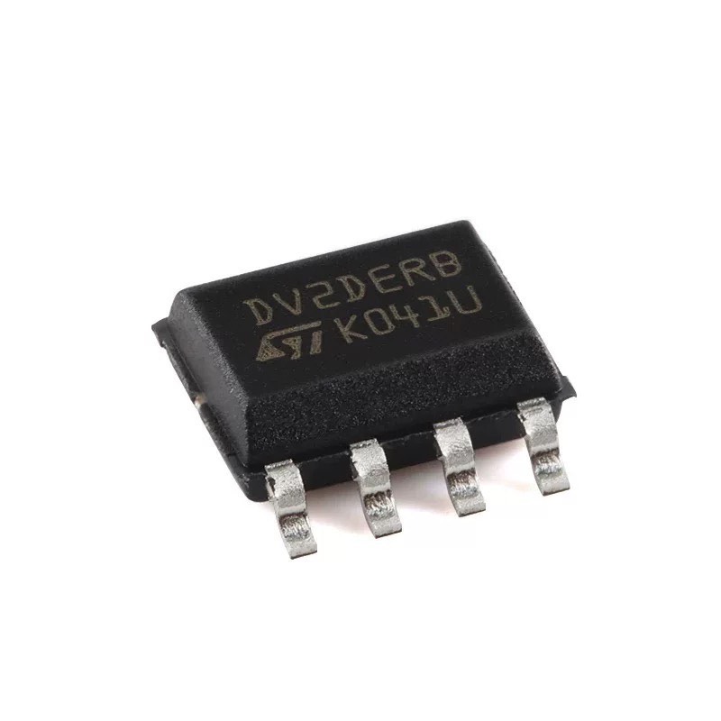
ST25DV04K-IER6S3 - 4Kbit Dynamic NFC/RFID Tag IC | STMicroelectronics
The ST25DV04K-IER6S3 is a dynamic NFC/RFID tag IC from STMicroelectronics, offering 4 Kbit of EEPROM memory with an I2C interface and an ISO 15693 / ISO 18000-3 Mode 1 compliant RF interface. It operates at 13.56 MHz and supports data rates up to 53 kbit/s in the RF interface, while the I2C interface supports up to 1 MHz. The device is housed in an SO-8 package (NXP-style) and is designed for applications requiring contactless data transfer and configuration, such as smart home devices, industrial equipment, and consumer electronics. Data verified as of 2026-08-05. What is a dynamic NFC/RFID tag IC? A dynamic NFC/RFID tag IC is a type of RFID transponder that combines a contactless RF interface with a wired interface (typically I2C) to allow a microcontroller to read and write the tag's memory both over the air and via the wired bus. This category sits within the broader hierarchy: NFC/RFID tag IC -> RFID transponder -> RFID/NFC integrated circuit -> wireless communication IC -> semiconductor. The dynamic nature means the tag can be updated in real time by the host MCU, enabling use cases like wireless configuration, data logging, and product authentication. Key features include 4 Kbit EEPROM organized in 128-byte pages, an I2C interface with a 1 MHz clock, an RF interface compliant with ISO 15693 and ISO 18000-3 Mode 1, a 64-bit unique identifier (UID), and an energy harvesting function that can power external circuits. The device supports a wide supply voltage range of 1.8V to 5.5V on the I2C side, and it includes an interrupt output to signal RF activity. The SO-8 package is compact and suitable for surface-mount assembly. Technically, the ST25DV04K-IER6S3 integrates an RF front-end with an analog-to-digital converter for energy harvesting, a state machine for protocol handling, and a memory controller for EEPROM access. The EEPROM is organized into 32 pages of 128 bits each, with a data retention of 10 years and an endurance of 1 million write cycles. The device supports both static and dynamic memory mapping, allowing the host to control which memory areas are accessible over RF. Typical applications include smart home devices (e.g., smart locks, thermostats), industrial equipment configuration, consumer electronics pairing (e.g., Bluetooth speakers, wearables), and medical device calibration. The energy harvesting feature enables battery-less operation for low-power sensors, and the I2C interface allows seamless integration with microcontrollers. When designing with this device, ensure proper antenna matching for the RF interface and place decoupling capacitors close to the VCC pin. The energy harvesting output should be buffered with a capacitor to provide stable power to external circuits. Also, consider the I2C address configuration via the RF field to avoid conflicts in multi-tag systems. This page synthesizes distributor pricing, drop-in alternatives, and practical design notes not found in the STMicroelectronics datasheet, providing a comprehensive resource for engineers evaluating the ST25DV04K-IER6S3.