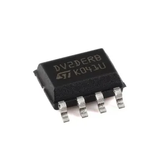
ADAR4002 - 0.5-19GHz Bidirectional TDU | Analog Devices
MPN: ADAR4002 ✓ Active| Qty | Unit Price | Extended |
|---|---|---|
| 1 | $150 | $150.00 |
| 10 | $135 | $1,350.00 |
| 100 | $120 | $12,000.00 |
| 500 | $105 | $52,500.00 |
| 1,000 | $90 | $90,000.00 |
ADAR4002 Overview
A true time delay unit (TDU) is a component that introduces a controlled delay to an RF signal, independent of frequency, which is essential for phased array beamforming and time-domain applications. Unlike phase shifters that only adjust phase, a TDU preserves signal integrity across wide bandwidths, making it critical for wideband systems. The ADAR4002 combines TDU and DSA functions, reducing component count and simplifying system design.
Key features include a wide operating frequency range of 0.5 GHz to 19 GHz, bidirectional operation, and low power consumption. The device supports both SPI and shift register control, with on-chip memory for 32 TDU and DSA states. The integrated sequencers allow fast bidirectional memory advance via the UPDATE pin, enabling rapid state changes. The 50 Ω matched ports simplify system integration, and the compact 14-lead WFDFN package supports space-constrained designs.
Technically, the ADAR4002 uses a combination of switched delay lines and attenuator stages to achieve precise time delay and attenuation. The bidirectional design allows signal flow in either direction, making it versatile for T/R modules. The SPI interface enables daisy chaining of multiple devices, and the shift register mode provides a simple parallel control option. The device operates over a wide temperature range, ensuring reliability in demanding environments.
Typical applications include phased array radar, electronic warfare, 5G beamforming, and test and measurement equipment. The wideband operation and bidirectional capability make it ideal for T/R modules in defense and communication systems. The low power consumption is beneficial for portable and battery-operated systems.
When designing with the ADAR4002, ensure proper RF layout and decoupling to maintain performance. The exposed pad should be soldered to a ground plane for thermal and electrical performance. The control interface should be configured according to system requirements, and the memory states should be programmed to achieve the desired delay and attenuation values.
Drop-in alternatives for ADAR4002 — same package, pin-to-pin compatible. Different-package parts requiring PCB rework are excluded.
Quick Comparison Tool — Select alternative parts for side-by-side comparison:
ADAR4002ACPZ-CSL
✅ Drop-In📋 Reference alternative (not in catalog)
ADAR4002 Specifications (manufacturer-published)
| Frequency Range | 0.5 GHz to 19 GHz |
| Type | True Time Delay Unit (TDU) with Digital Step Attenuator (DSA) |
| Channels | 1 |
| Bidirectional | Yes |
| Impedance | 50 Ω |
| Control Interface | SPI or Shift Register |
| Memory States | 32 TDU and DSA states |
| Package | 14-WFDFN Exposed Pad, CSP |
| Mounting Type | Surface Mount |
| RoHS Status | Compliant (per Analog Devices) |
ADAR4002 Pin Configuration
| Pin 1 | RF1 — RF port 1 |
| Pin 2 | GND — Ground |
| Pin 3 | RF2 — RF port 2 |
| Pin 4 | VDD — Power supply |
| Pin 5 | SCLK — SPI clock |
| Pin 6 | SDI — SPI data input |
| Pin 7 | SDO — SPI data output |
| Pin 8 | CS — Chip select |
| Pin 9 | UPDATE — Update pin for memory advance |
| Pin 10 | GND — Ground |
| Pin 11 | GND — Ground |
| Pin 12 | GND — Ground |
| Pin 13 | GND — Ground |
| Pin 14 | GND — Ground |
Typical Applications
ADAR4002 is suitable for 6 applications: Phased Array Radar, Electronic Warfare, 5G Beamforming, Test and Measurement, Satellite Communication, Radar Test Systems.
Phased Array Radar
The ADAR4002 provides true time delay for beam steering in phased array radar systems. Its wideband operation (0.5-19 GHz) and bidirectional capability make it ideal for T/R modules. The low power consumption is beneficial for large arrays. The SPI interface allows precise control of delay and attenuation for each element.
Recommended
Electronic Warfare
In electronic warfare, the ADAR4002 is used for signal delay and attenuation to simulate or counter threats. Its wideband frequency range and fast state switching via the UPDATE pin enable rapid response. The bidirectional operation supports both receive and transmit paths, making it versatile for EW systems.
Recommended
5G Beamforming
The ADAR4002 is suitable for 5G beamforming, where true time delay is required to maintain signal integrity across wide bandwidths. Its 0.5-19 GHz range covers sub-6 GHz and mmWave bands. The compact package and low power consumption are ideal for small cell and massive MIMO systems.
Recommended
Test and Measurement
The ADAR4002 can be used in test equipment to introduce precise time delays and attenuation for calibration and characterization. Its SPI interface allows automated control, and the 50 Ω matched ports simplify integration into test setups. The wideband operation supports a variety of RF measurements.
Recommended
Satellite Communication
In satellite communication, the ADAR4002 provides time delay and attenuation for beamforming and signal conditioning. Its wideband operation covers C, X, Ku, and Ka bands. The low power consumption is critical for space-constrained satellite payloads.
Recommended
Radar Test Systems
The ADAR4002 is used in radar test systems to simulate target echoes with precise time delay and attenuation. Its bidirectional operation allows testing of both transmit and receive paths. The memory states enable pre-programmed scenarios for automated testing.
Recommended
Recommended Products Summary
Engineering reference data for ADAR4002 — comparison, design guidance, and compliance information.
Selection Guide
Comparison with Alternatives
| Parameter | This Product | ADAR4002ACPZ-CSL | ADAR4001 |
|---|---|---|---|
| Package | 14-WFDFN Exposed Pad, CSP | 14-WFDFN Exposed Pad, CSP | Different package |
| Brand | Analog Devices | Analog Devices | Analog Devices |
| Channels | 1 | 1 | 4 |
Key Differentiators
- Wideband operation up to 19 GHz (vs ADAR4001)
- Single-channel design (vs ADAR4001)
- Bidirectional operation (vs ADAR4001)
Design Notes
Ensure proper RF layout with 50 Ω controlled impedance traces for RF1 and RF2 ports. Place decoupling capacitors close to the VDD pin and use a solid ground plane. The exposed pad should be soldered to the ground plane for thermal and electrical performance.
The ADAR4002 is a low power device, but ensure the supply voltage is within the recommended range. Use a low-noise LDO to power the device to avoid noise coupling into the RF path. Decouple the supply with 100 nF and 10 µF capacitors.
Avoid exceeding the maximum frequency range of 19 GHz. Ensure the control interface (SPI or shift register) is correctly configured to avoid unintended state changes. The UPDATE pin should be used carefully to advance memory states only when needed.
Compliance Information
RoHS compliance per Analog Devices product page. Other compliance data not specified in provided data.