ADC/DAC
بەرهەمەکان (3,600+)
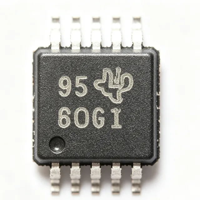
ADS1115IDGSR - 16-Bit I2C ADC with PGA | TI | Sensor Nodes
The Texas Instruments ADS1115IDGSR is a precision, low-power, 16-bit delta-sigma analog-to-digital converter (ADC) with an I2C-compatible interface, supplied in a 10-pin VSSOP (DGS) package. It integrates a programmable gain amplifier (PGA), a low-drift voltage reference, an internal oscillator, and a digital comparator, enabling compact high-resolution measurement systems with minimal external components. An analog-to-digital converter (ADC) is a mixed-signal device that translates continuous analog voltages into discrete digital codes that microcontrollers and processors can interpret. The ADS1115 operates as a sigma-delta ADC, using oversampling and noise shaping to achieve 16-bit resolution at conversion rates up to 860 samples per second (SPS). Within the signal-chain hierarchy, it belongs to precision data-acquisition ICs and eliminates the need for an external reference or clock source. Key features include four single-ended or two differential input channels via an input multiplexer, a PGA with gains from 2/3 to 16 V/V, an I2C interface supporting four bus addresses (0x48 through 0x4B), and an onboard comparator with ALERT/conversion-ready output. The device operates from a 2.0V to 5.5V supply over -40C to +125C, drawing only about 150 uA of supply current in continuous mode. The ADS111x architecture uses a delta-sigma modulator followed by a digital decimation filter for high accuracy at low power. The integrated PGA amplifies small sensor signals before conversion to improve effective resolution, while the low-drift internal reference keeps industrial measurements stable over time and temperature. The lead-free VSSOP-10 package (3.00mm width) suits space-constrained PCB layouts. Typical applications include battery voltage and current monitoring, portable instrumentation, IoT sensor nodes, temperature and pressure measurement, and industrial process control. Because no external reference or oscillator is required, the ADS1115IDGSR reduces BOM complexity in designs needing 16-bit accuracy on an I2C bus. For best performance, place a 0.1uF decoupling capacitor close to VDD and use the ADDR pin to avoid I2C bus conflicts. Keep source impedance low enough to charge the sampling capacitor; a low-noise LDO such as TPS7A26-Q1 further improves measurement stability.

ADS1115IDGSR-Q1 - 16-Bit I2C ADC, 860SPS | Texas Instruments
The Texas Instruments ADS1115IDGSR-Q1 is a precision, low-power, 16-bit, I2C-compatible delta-sigma analog-to-digital converter (ADC) in a 10-pin VSSOP (DGS) package, qualified to AEC-Q100 for automotive applications. It integrates a 4-channel input multiplexer, a programmable gain amplifier (PGA), a low-drift internal voltage reference, an internal oscillator, and a digital comparator, enabling compact single-chip signal acquisition. An ADC (analog-to-digital converter) is a mixed-signal device that converts continuous analog voltages into discrete digital values. Within the converter hierarchy, the ADS1115 is a delta-sigma (over-sampling) ADC, a topology prized for high resolution and low noise at modest sample rates, sitting above SAR ADCs in resolution and below integrating ADCs in speed. It connects to any host MCU or processor via an I2C bus, making it a power-management and sensor-measurement building block. Key features include 16-bit resolution with up to 860 samples per second (SPS) conversion rate, an I2C interface supporting four selectable addresses, and a PGA with gain settings that allow full-scale ranges down to the +/-256 mV range for direct connection of small signals. The integrated digital comparator supports alert-based operation, reducing host polling overhead. Conversion rate and duty cycling support low average power consumption in battery-backed systems. The delta-sigma architecture oversamples the input and applies digital decimation filtering, yielding excellent linearity and noise performance without external precision components. Because reference, oscillator, and PGA are on-chip, external BOM count stays minimal and channel-to-channel measurements remain consistent. Typical applications include automotive battery-voltage and current monitoring, sensor measurement in body and chassis modules, battery management systems (BMS) auxiliary sensing, factory automation analog input modules, and precision portable instrumentation. The Q1 qualification makes it a natural fit alongside TI automotive power and monitoring devices. Design tip: the input pins must not exceed VDD + 0.3V; for measuring rails above the supply, use a resistive divider and match the source impedance to the PGA input requirements to preserve accuracy.

ADS1118IDGSR - 16-Bit 860-SPS 4-Channel ADC | TI
The Texas Instruments ADS1118IDGSR is a 16-bit, 860-SPS, 4-channel delta-sigma analog-to-digital converter with a programmable gain amplifier, integrated voltage reference, oscillator, temperature sensor, and SPI interface, housed in a 10-VSSOP package. It is designed for low-power precision measurement systems and supports analog sensor inputs as well as temperature sensing. An ADC converts continuous analog voltage into a numeric value for processing, measurement, or control. The ADS1118 belongs to the delta-sigma ADC class, where an internal modulator and digital filter shape the conversion result. Its integrated PGA allows low-level sensor signals to be amplified before conversion, while the internal reference, oscillator, and temperature sensor reduce the number of external support components required in compact measurement designs. The main headline specifications are 16-bit resolution, conversion rates up to 860 samples per second, four analog input channels, and operation across a -40°C to +125°C temperature range. The device supports SPI-compatible serial communication and is offered in a small 10-pin VSSOP package. The integrated reference and temperature sensor are especially useful for sensor measurements, thermocouple-related monitoring, and systems requiring a compact analog front end. The delta-sigma architecture provides high resolution for low-frequency and slowly changing signals, while the programmable gain amplifier supports a range of input amplitudes. The internal oscillator allows operation without an external clock, which can simplify PCB design and reduce component count. The ADC is suitable when deterministic digital readout, modest conversion speed, and low power consumption are more important than very high sample rates. Typical applications include industrial process monitoring, temperature sensing, pressure and strain-signal acquisition, portable instrumentation, environmental measurement, and low-power embedded sensing. The integrated temperature sensor can provide a local temperature reading, while the analog channels support external sensors such as thermistors, resistive bridges, potentiometers, and other slowly varying analog sources. A key design consideration is analog signal conditioning and PCB layout. The sensor input must stay within the ADC input range, and the PGA gain must be selected so that the conditioned signal uses the converter’s available resolution without overloading the input. Decoupling capacitors should be placed close to the power pins, and the analog and digital return paths should be arranged to minimize noise coupling into the measurement channels. The 860-SPS maximum rate also means that applications requiring faster sampling need a different ADC architecture. This page combines the manufacturer’s published ADS1118 features, distributor pricing and availability signals, package information, application guidance, and drop-in replacement analysis for engineers evaluating the ADS1118IDGSR.

ADS1118QDGSRQ1 - 16-bit 860SPS Automotive Delta-Sigma ADC | TI
The Texas Instruments ADS1118QDGSRQ1 is an automotive-qualified, precision, low-power, 16-bit, 860-SPS, 4-channel, delta-sigma analog-to-digital converter (ADC) that integrates a programmable gain amplifier (PGA), voltage reference, internal oscillator, high-accuracy temperature sensor, and an SPI-compatible serial interface in a 10-pin VSSOP (DGS) package. It provides 4 single-ended or 2 differential input channels, supports a wide 2.0 V to 5.5 V analog supply range, and delivers up to 16 bits of effective resolution across data rates from 8 SPS to 860 SPS, with an integrated PGA offering gains of 1, 2, 4, 8, 16, 32, 64, and 128 to accommodate low-level sensor signals. A delta-sigma ADC is a type of oversampling converter that uses noise shaping and digital filtering to achieve high resolution and excellent noise rejection at low frequencies. In the broader taxonomy it sits under: ADC -> data converter -> signal chain IC -> mixed-signal semiconductor. The ADS1118-Q1 is the automotive (-Q1) variant of the industrial ADS1118 family, designed for AEC-Q100 qualified applications where robust thermal, EMI, and reliability performance is mandatory. Key features include an integrated low-drift voltage reference (typically 4.096 V with 0.01 %/°C drift), an on-chip temperature sensor with 0.5 °C typical accuracy, a low quiescent current of typically 150 µA in continuous-conversion mode, and a power-down current below 1 µA. The internal PGA eliminates the requirement for an external instrumentation front-end in many bridge sensor applications. The SPI-compatible interface supports up to 4-wire connections and allows daisy-chaining of multiple devices. Typical applications include automotive sensor monitoring (battery management systems, cabin climate, occupant detection), industrial process control (4-20 mA loop digitization, RTD/thermocouple digitization), portable instrumentation, and temperature-compensated measurement chains. The wide supply range and small footprint make it ideal for space-constrained designs. When designing with this device, place the supply decoupling capacitor within 5 mm of the AVDD pin and keep digital traces away from analog inputs. The -Q1 suffix guarantees operation from -40 °C to +125 °C and AEC-Q100 Grade 1 qualification for automotive use cases.

ADS1130IPW - 18-Bit, 80SPS Bridge-Sensor ADC | Texas Instruments
Texas Instruments ADS1130IPW is a precision 18-bit, single-channel delta-sigma analog-to-digital converter optimized for resistive bridge sensors, with an 80 SPS conversion rate and a 16-pin TSSOP package. It integrates a low-noise gain amplifier, onboard oscillator, and precision 18-bit delta-sigma ADC to form a complete front end for strain gauges, weigh scales, and similar bridge-sensor systems. A sigma-delta ADC is a voltage-regulating data-converter category that uses continuous-time oversampling and digital filtering to provide high resolution and excellent rejection of low-frequency noise. The ADS1130 belongs to the ADC hierarchy, combining a low-noise analog gain stage with a delta-sigma conversion core and serial interface. This integration reduces the number of external precision components required in a bridge measurement circuit. The principal operating characteristics include 18-bit resolution, 80 SPS throughput, one differential input channel, and a programmable low-noise gain amplifier. The integrated oscillator supports a complete measurement front end without an external clock source. According to the Texas Instruments ADS1130 datasheet, the device is specifically designed for resistive bridge sensors and weigh-scale applications rather than general-purpose high-speed waveform conversion. The delta-sigma architecture prioritizes resolution and noise performance over conversion latency. Digital filtering suppresses broadband and low-frequency noise while averaging successive conversions, making the converter appropriate for slowly changing force, pressure, or strain signals. The onboard gain amplifier conditions the small differential output generated by a Wheatstone bridge before conversion, while the internal reference and oscillator support repeatable measurement operation. Typical uses include electronic weighing systems, strain-gauge instrumentation, industrial force sensing, pressure transmitters, and laboratory measurement equipment. In a weigh-scale design, the bridge output can be connected directly to the differential input, with the excitation voltage and signal ground referenced carefully to minimize common-mode errors and thermoelectric offsets. A critical design consideration is the relationship between bridge excitation, input range, gain, and allowable overvoltage. Confirm the selected gain and excitation voltage against the maximum bridge output and the device electrical limits before calibration. Place filtering and protection components where they will not disturb sensitive bridge routing, and route analog and digital return currents separately to reduce measurement error. This product page combines the manufacturer's key device characteristics with practical application guidance, package information, sourcing instructions, and a careful review of drop-in replacement evidence. The replacement analysis deliberately distinguishes confirmed interchangeability from devices that merely use a similar package or function, helping engineers avoid PCB, interface, and calibration risks.

ADS1131ID - 18-Bit Delta-Sigma ADC | Texas Instruments
Texas Instruments ADS1131ID is an 18-bit, single-channel delta-sigma analog-to-digital converter operating at 80 samples per second. Designed as a complete front end for resistive bridge sensors, it integrates a low-noise amplifier with a gain of 64, an internal oscillator, and a low-side power switch for bridge excitation. The device is supplied in a 16-pin SOIC package and is specified for an industrial temperature range of -40°C to +85°C. An analog-to-digital converter converts an analog input voltage into a numeric value for processing by a microcontroller or other digital controller. The ADS1131ID belongs to the delta-sigma ADC family and combines an analog signal-conditioning path with a precision 18-bit conversion stage. Its integrated bridge-switch feature is particularly useful in weighing systems because it can control the excitation current applied to a Wheatstone bridge while keeping the analog measurement path close to the sensor. The principal device characteristics include 18-bit resolution, an 80-SPS conversion rate, one analog input, and a single-ended or differential input architecture. The internal amplifier provides a gain of 64, reducing the need for external analog gain stages in typical bridge-sensor circuits. An internal oscillator reduces dependence on an external clock source, while dedicated configuration pins simplify control because the device has no digital registers to program. The converter outputs data through a serial interface suitable for connection to an MSP430 or another microcontroller. Dedicated pins control conversion timing and operating states, allowing the host processor to request data without writing a lengthy register sequence. This pin-programmed architecture can reduce firmware complexity and make the measurement interface easier to isolate on a mixed-signal printed circuit board. Typical applications include resistive weigh scales, industrial load cells, pressure transmitters, and other bridge-based measurement systems. The combination of an integrated bridge power switch, low-noise amplifier, internal oscillator, and 18-bit conversion result supports compact sensor modules where component count and PCB area are important. The device can also form the analog front end of portable weighing equipment when low power consumption and deterministic control are priorities. When designing the analog front end, verify the bridge excitation requirements, sensor input range, gain, conversion timing, and digital-interface voltage levels against the manufacturer datasheet. Pay particular attention to the power-switch configuration, analog input filtering, grounding, and the relationship between the bridge output and the converter input range. The 16-SOIC footprint requires adequate copper around thermal and return paths even though the principal measurement accuracy depends more heavily on the bridge, reference strategy, layout, and calibration than on package size. This product page combines the manufacturer's device description with practical application guidance, sourcing information, and a parameter-by-parameter comparison framework. It also identifies the uncertainty that remains when a complete public pin description, verified alternative list, and explicit quantity-break price are unavailable, allowing engineers to focus on the validated ADS1131ID function, resolution, conversion rate, package, and bridge-sensor role.
ADS1131IDR - 18-Bit Delta-Sigma ADC | Texas Instruments (Tape & Reel)
Texas Instruments ADS1131IDR is an 18-bit, single-channel delta-sigma analog-to-digital converter operating at 80 samples per second. Designed as a complete front end for resistive bridge sensors, it integrates a low-noise amplifier with a gain of 64, an internal oscillator, and a low-side power switch for bridge excitation. The device is supplied in a 16-pin SOIC package and is specified for an industrial temperature range of -40°C to +85°C. An analog-to-digital converter converts an analog input voltage into a numeric value for processing by a microcontroller or other digital controller. The ADS1131IDR belongs to the delta-sigma ADC family and combines an analog signal-conditioning path with a precision 18-bit conversion stage. Its integrated bridge-switch feature is particularly useful in weighing systems because it can control the excitation current applied to a Wheatstone bridge while keeping the analog measurement path close to the sensor. The principal device characteristics include 18-bit resolution, an 80-SPS conversion rate, one analog input, and a single-ended or differential input architecture. The internal amplifier provides a gain of 64, reducing the need for external analog gain stages in typical bridge-sensor circuits. An internal oscillator reduces dependence on an external clock source, while dedicated configuration pins simplify control because the device has no digital registers to program. The converter outputs data through a serial interface suitable for connection to an MSP430 or another microcontroller. Dedicated pins control conversion timing and operating states, allowing the host processor to request data without writing a lengthy register sequence. This pin-programmed architecture can reduce firmware complexity and make the measurement interface easier to isolate on a mixed-signal printed circuit board. Typical applications include resistive weigh scales, industrial load cells, pressure transmitters, and other bridge-based measurement systems. The combination of an integrated bridge power switch, low-noise amplifier, internal oscillator, and 18-bit conversion result supports compact sensor modules where component count and PCB area are important. The device can also form the analog front end of portable weighing equipment when low power consumption and deterministic control are priorities. When designing the analog front end, verify the bridge excitation requirements, sensor input range, gain, conversion timing, and digital-interface voltage levels against the manufacturer datasheet. Pay particular attention to the power-switch configuration, analog input filtering, grounding, and the relationship between the bridge output and the converter input range. The 16-SOIC footprint requires adequate copper around thermal and return paths even though the principal measurement accuracy depends more heavily on the bridge, reference strategy, layout, and calibration than on package size. This product page combines the manufacturer's device description with practical application guidance, sourcing information, and a parameter-by-parameter comparison framework. It also identifies the uncertainty that remains when a complete public pin description, verified alternative list, and explicit quantity-break price are unavailable, allowing engineers to focus on the validated ADS1131IDR function, resolution, conversion rate, package, and bridge-sensor role.

ADS114S08BIPBSR - 16-Bit 4kSPS 12-Ch Delta-Sigma ADC | TI
The Texas Instruments ADS114S08BIPBSR is a 16-bit, 4-kSPS, 12-channel delta-sigma (ΔΣ) analog-to-digital converter with an integrated programmable gain amplifier (PGA) and voltage reference, supplied in a 32-pin TQFP (PBS) package measuring 5x5 mm. It is optimized for low-cost sensor measurement applications and consumes as little as 280 µA of supply current, which makes it appropriate for battery-powered or thermally constrained systems. The integrated PGA accepts gains from 1 to 128 V/V, allowing direct interface to low-output sensors such as load cells, thermocouples, and bridge-type pressure transducers without external amplification. A delta-sigma ADC is a noise-shaping converter that oversamples the analog input at a rate many times higher than the Nyquist frequency of the output data rate, then shapes quantization noise out of the baseband and decimates the bitstream to produce a high-resolution result. Within the broader data-converter hierarchy, the ADS114S08B occupies the precision-low-speed node between successive-approximation register (SAR) ADCs and wider-bandwidth delta-sigma parts, positioning it as a power management and signal-chain IC for measurement-grade instrumentation. Key specifications include a maximum data rate of 4 kSPS, simultaneous 50 Hz / 60 Hz line-frequency rejection at data rates of 20 SPS or lower, a low-latency digital filter, on-chip temperature sensor, and an SPI-compatible serial interface. The internal voltage reference is selectable between an internal 2.5 V source and an external reference, supporting ratiometric and absolute measurement topologies. Twelve analog input channels can be configured as differential, pseudo-differential, or single-ended, providing flexibility for multi-sensor designs. The device architecture pairs a chopper-stabilized input front end with a second-order delta-sigma modulator and a programmable SINC3 digital filter. Chopper stabilization reduces the 1/f noise corner and corrects input-offset drift over temperature, while the SINC3 filter gives first-cycle conversion latency at low data rates, useful for closed-loop control applications. The internal PGA gain of up to 128 V/V combined with the low input-referred noise allows the ADC to resolve microvolt-level signals directly. Typical applications include weigh scales, strain-gauge bridge sensors, thermocouple temperature measurement, RTD signal conditioning, industrial process-control analog input modules, and portable medical instrumentation such as blood-pressure monitors and body-composition analyzers. The wide analog supply range of 2.7 V to 5.25 V and digital supply range of 2.7 V to 3.6 V let it pair directly with 3.3 V MCUs and 5 V analog signal chains. When designing with this ADC, evaluate total input-referred noise against the target data rate because the SINC3 filter trades bandwidth for resolution - selecting a 2.5 SPS or 20 SPS output rate improves effective resolution to 16-bit noise-free codes for weigh-scale applications. Decouple AVDD and DVDD with 1 µF and 100 nF ceramic capacitors placed within 2 mm of the supply pins to keep digital switching noise out of the modulator. This page synthesizes distributor pricing, same-brand drop-in alternatives, and practical design notes not found in the standalone manufacturer datasheet, providing engineers with a single reference for selection, replacement, and PCB layout decisions.

ADS114S08BIRHBR - 16-bit 4kSPS 12-ch Delta-Sigma ADC | Texas Instruments
The Texas Instruments ADS114S08BIRHBR is a 16-bit, 4-kSPS, 12-channel, delta-sigma analog-to-digital converter with integrated PGA and 2.5 V voltage reference, housed in a 32-pin VQFN (RHB) 5x5 mm package with exposed thermal pad. It delivers 16-bit resolution at up to 4 kSPS data rate, consumes as little as 280 µA, and provides programmable gain from 1 to 128. A delta-sigma ADC is a type of analog-to-digital converter that uses oversampling and noise shaping to achieve high resolution at low sample rates. Delta-sigma ADCs are a subset of integrating ADCs, which fall under the broader category of data converters, mixed-signal ICs, and finally semiconductors. The ADS114S08B sits in this taxonomy between precision SAR ADCs (single-shot, medium speed) and wideband pipeline ADCs (high speed, lower resolution). Delta-sigma converters dominate low-frequency precision measurement - sensor signal conditioning, weigh scales, temperature, strain gauge bridges - because their noise-shaping topology yields 16-24 effective bits at bandwidths below a few kHz. Key features include 12 analog input channels with low-noise PGA gains of 1, 2, 4, 8, 16, 32, 64, and 128, programmable data rates from 2.5 SPS to 4 kSPS, simultaneous 50-Hz and 60-Hz line rejection at data rates up to 20 SPS, an integrated 2.5 V low-drift voltage reference, and two matched excitation current sources for RTD and bridge sensor biasing. The device offers low-latency digital filter response, an SPI-compatible serial data interface, and an operating supply current as low as 280 µA in low-power mode. Architecture-wise, the ADS114S08B uses a 2nd-order delta-sigma modulator followed by a programmable SINC + FIR digital decimation filter. The modulator clock is derived from an internal oscillator; the digital filter provides both single-cycle and FIR modes. The integrated PGA delivers gains up to 128 V/V, allowing direct interface to thermocouples and strain-gauge bridges without external instrumentation amplifiers. The integrated low-drift 2.5 V reference eliminates an external reference IC for cost-sensitive designs. Typical applications include weigh scales and load cell digitizers, RTD and thermocouple temperature acquisition, strain-gauge bridge measurement, industrial process control analog input modules, factory automation sensor interfaces, and battery-powered portable sensor instruments. The 280 µA quiescent current makes it well suited for battery-powered or loop-powered 4-20 mA sensor transmitters where total analog-section power budget is constrained. When designing with the ADS114S08B, allocate GPIO on the host microcontroller for /DRDY, /CS, SCLK, DIN, DOUT/DRDY, and /RESET. Use a clean low-noise analog supply with a ferrite bead separating it from the digital 3.3 V rail. Place the 0.10 µF + 10 µF decoupling pair within 5 mm of the AVDD pin. The exposed thermal pad (pin 33) must be soldered to a continuous analog ground plane for thermal and EMI performance.
ADS1201U - 24-Bit 1 kSPS Delta-Sigma ADC | Texas Instruments
The Texas Instruments ADS1201U is a 24-bit high-dynamic-range delta-sigma modulator with a fully differential input, 1 kSPS conversion rate, and two-wire serial interface in a 16-pin SOIC package. It supports internal or external voltage references and includes on-chip switches for calibration, making it suitable for precision analog measurement systems requiring high dynamic range and low-noise signal acquisition. A delta-sigma ADC is a signal-conversion IC that uses oversampling, noise shaping, and digital filtering to convert an analog input into a high-resolution digital result. Within the ADC hierarchy, the ADS1201U belongs to the delta-sigma modulator family, provides analog-to-digital conversion, and ultimately functions as a precision data-conversion IC. Its fully differential architecture is particularly useful when the source has a small voltage across a common-mode range and benefits from rejection of common-mode noise. Key features include a nominal 24-bit resolution, a 1 kSPS data rate, and approximately 130 dB of dynamic range. The two-wire interface reduces the number of serial connections required between the converter and a controller. The differential input supports single-ended or differential source arrangements when paired with suitable front-end circuitry, while selectable internal or external references allow the reference voltage to be matched to the transducer and analog signal chain. The delta-sigma architecture trades conversion speed for resolution and noise performance. It is most effective for slowly changing or precision-oriented signals rather than high-bandwidth waveform acquisition. The on-chip calibration switches support system-level calibration, and the 16-pin SOIC package permits assembly using conventional surface-mount production methods. Maximum power dissipation is reported as 40 mW, making thermal design relatively manageable in typical precision-measurement equipment. Typical uses include pressure and load-cell signal conditioning, industrial sensor acquisition, instrumentation amplifiers, weigh systems, and low-frequency measurement front ends. A controller can read the serial output and perform digital filtering or scaling as required by the measurement system. The differential input can also front-end sensor bridges where preserving signal integrity and rejecting common-mode disturbances are priorities. Designers should verify the required analog bandwidth, digital-filter settling time, reference configuration, and serial timing before fixing the system sampling strategy. Input protection, reference bypassing, and a quiet ground layout are important because they can affect achievable resolution. The 40 mW maximum power dissipation rating provides a useful starting point, but actual board-level thermal behavior should be checked against the final operating conditions. This page consolidates verified manufacturer and distributor information, lifecycle context, candidate replacements, and practical selection guidance. It also distinguishes confirmed device attributes from parameters that still require verification, helping engineers shorten datasheet review and replacement-planning time without inventing unavailable electrical details.
ADS1201U-1 - 24-Bit 1ksps Modulator | Texas Instruments
The Texas Instruments ADS1201U-1 is a high-dynamic-range, single-channel 24-bit delta-sigma modulator with a maximum output data rate of 1 ksps, housed in a 16-pin SOIC package. It converts a differential analog input into a high-resolution serial bitstream suitable for precision measurement, signal isolation, and sensor-interface systems. A delta-sigma modulator is the first stage of a delta-sigma analog-to-digital conversion chain. It uses continuous-time oversampling and digital filtering to shape quantization noise away from the signal band. When paired with a suitable digital filter, this architecture can deliver high resolution and excellent noise performance from a low-bandwidth measurement such as pressure, temperature, load-cell, or industrial process control. The ADS1201U-1 belongs to the broader ADC/DAC and data-acquisition semiconductor hierarchy. The primary identified characteristics are 24-bit resolution, operation up to 1 ksps, a differential analog input, and a serial two-wire digital interface. These features make the device appropriate for compact measurement systems in which the host processor or dedicated digital filter performs subsequent decimation and data transfer. The 16-pin SOIC package supports conventional surface-mount assembly and provides a practical upgrade path from older ADS1201 configurations. The delta-sigma architecture prioritizes resolution and noise performance for low-frequency or narrow-bandwidth signals rather than high-rate waveform capture. Its 1 ksps ceiling limits throughput relative to SAR converters, but the architecture supports precise extraction of low-level information from a narrow measurement band. Digital decimation and sinc-type filtering are therefore central to obtaining the intended effective resolution and usable conversion speed. Typical applications include isolated current and voltage measurement, precision weighing systems, industrial process instrumentation, and low-bandwidth sensor conditioning. In each case, the differential input structure can support rejection of common-mode disturbance when paired with appropriate input circuitry, while the serial output can connect to a microcontroller, DSP, FPGA, or dedicated digital filter. Designers should follow the manufacturer datasheet for the exact input range, supply requirements, clocking method, digital-interface timing, and bypass-network values. Input filtering, reference stability, grounding, and digital-interface layout can materially affect achievable noise performance. Confirm that the required output rate and filter bandwidth fit the intended measurement bandwidth before committing the device to a precision signal chain. This page combines the verified ADS1201U-1 device identity and packaging details with replacement guidance, application-specific engineering context, and design considerations. It focuses on the practical role of the 24-bit, 1 ksps delta-sigma modulator while clearly separating confirmed characteristics from parameters that require confirmation from the manufacturer datasheet.
ADS1201U/1K - 24-Bit 1kSPS Delta-Sigma ADC | Texas Instruments
The Texas Instruments ADS1201U/1K is a 24-bit high-dynamic-range delta-sigma modulator with a 1 kSPS nominal sampling rate, housed in a 16-pin SOIC package. It is designed for high-resolution measurement systems that use an external digital filter to convert the serial modulator output into a filtered digital result. The device supports industrial instrumentation, precision sensor measurement, and isolated or noisy analog environments where oversampling and digital filtering improve signal-to-noise performance. A delta-sigma ADC is a type of analog-to-digital converter that uses oversampling, noise shaping, and digital decimation to achieve high resolution. In the broader hierarchy, the ADS1201U/1K belongs to the ADC/DAC category, specifically the high-dynamic-range delta-sigma modulator class. It is commonly positioned ahead of a digital filter or microcontroller in a measurement signal chain. The key specifications are 24-bit nominal resolution, a 1 kSPS sampling rate, and a serial interface. These features make the converter appropriate for slow, precision-oriented measurements rather than high-bandwidth waveform acquisition. The modulator architecture helps reduce the influence of quantization noise within the selected digital-filter bandwidth, while the serial output supports compact embedded systems and programmable filter implementations. The ADS1201U/1K is identified as an industrial-use component with a nominal 5 V supply and an operating temperature range of -40 °C to +85 °C. Its 16-pin SOIC package supports conventional surface-mount assembly. The device operates as a modulator rather than as a conventional standalone ADC with an integrated digital decimation filter, so system performance depends strongly on the selected digital filter, clocking arrangement, reference implementation, and analog input conditioning. Typical applications include precision bridge and load-cell measurements, industrial pressure and temperature acquisition, low-frequency sensor monitoring, and measurement systems requiring a clean serial output for later digital filtering. In each case, the 1 kSPS rate favors applications whose useful information bandwidth is much lower than the raw modulator clock rate. A critical design consideration is input and reference stability. Use appropriate low-noise decoupling, keep analog and digital return currents separated, and design the digital decimation filter for the intended output bandwidth. Confirm clock frequency, bit timing, and serial interface levels against the manufacturer datasheet before releasing the PCB. This page combines the component identity, verified distributor observations, package information, application guidance, and drop-in replacement analysis to support faster engineering evaluation and sourcing decisions.
ADS1201UG4 - 24-Bit 1 kSPS Delta-Sigma ADC | Texas Instruments
The Texas Instruments ADS1201UG4 is a 24-bit, 1 kSPS delta-sigma modulator ADC with a serial interface, supplied in a 16-pin SOIC package. It operates from 4.75 V to 5.25 V and is designed for precision signal conversion where high resolution, low power consumption, and compact implementation are more important than high-speed sampling. The industrial-temperature device uses a 0.295-inch, 7.50 mm-wide gull-wing package. A delta-sigma ADC is a type of analog-to-digital converter that oversamples its input and uses digital filtering and noise shaping to deliver high effective resolution. Within the data-converter hierarchy, the ADS1201UG4 combines a sigma-delta modulator with an integrated digital filter, making it suitable for sensors and instrumentation signals that can be sampled at relatively low rates. Its serial output reduces the number of PCB traces required in space-constrained designs. The principal characteristics are 24-bit nominal resolution, a 1 kSPS maximum sampling rate, a serial interface, and a single 4.75 V to 5.25 V analog supply range. These specifications suit bridge sensors, pressure transducers, temperature measurement systems, and other slowly changing analog signals. The industrial temperature grade supports use across extended commercial and industrial ambient conditions when the complete circuit is designed for the same environmental range. Technically, the converter prioritizes effective resolution and noise performance rather than conversion latency or multiplexing. A 1 kSPS conversion rate is sufficient for many instrumentation, weighing, process-control, and low-frequency sensor applications. The serial interface allows the converter to communicate with a microcontroller or digital signal controller while keeping the external footprint compact. Designers should treat the ADC as a precision measurement element whose usable accuracy also depends on reference quality, input conditioning, grounding, and digital filtering. Typical uses include industrial pressure and flow instrumentation, strain-gauge and load-cell signal chains, temperature measurement, low-frequency vibration monitoring, and embedded data-acquisition systems. The device can reduce the need for a separate low-noise front end when the input bandwidth is appropriately limited. Its 16-pin SOIC package also simplifies assembly compared with leadless packages requiring a thermal-pad land pattern. The principal design consideration is power-supply cleanliness. A 5 V analog rail should be decoupled close to the supply pins, the analog and digital return paths should be managed carefully, and the voltage reference must remain stable throughout measurement. Follow the pin-description and layout guidance in the manufacturer datasheet when assigning nets and grounding the exposed system board. This page combines the exact ADS1201UG4 package and conversion characteristics, procurement guidance, lifecycle context, replacement considerations, and practical PCB design notes to help engineers evaluate this precision delta-sigma ADC before integrating it into a measurement design.
ADS1208IPW - 10MHz Hall Sensor Modulator | Texas Instruments
Texas Instruments ADS1208IPW is a 10MHz second-order delta-sigma modulator with built-in current excitation for Hall sensors. It provides a specified differential input range of ±100mV, a ±125mV full-scale range, 95dB typical common-mode rejection, and 82dB typical signal-to-noise ratio. The device uses a 16-bit, 40kSPS serial output in a 16-pin TSSOP package. A delta-sigma modulator is an analog-to-digital conversion technique that shapes quantization noise toward higher frequencies and uses digital filtering to produce high-resolution data. The ADS1208 belongs to the special-purpose ADC hierarchy, combining a low-noise analog front end, Hall-element excitation circuitry, and a serial digital interface. Its architecture is intended to preserve weak magnetic-sensor signals while rejecting common-mode voltage and noise coupled into the sensor wiring. The principal features are adjustable excitation current for sensor biasing, digital output compatibility with the ADS1202 and ADS1203, and a separate digital supply operating from 2.7V to 5.5V. The specified ±100mV input range supports magnetic signals generated directly by Hall elements, while the 95dB typical common-mode rejection helps isolate small differential outputs from supply and environmental interference. The second-order delta-sigma signal path provides 16-bit resolution at a 40kSPS data rate. This combination favors current sensing, magnetic-field measurement, position detection, and industrial instrumentation rather than high-bandwidth waveform acquisition. Because the ADS1208 is a modulator rather than a conventional general-purpose ADC, downstream filtering, clocking, decimation, and digital signal processing are central to obtaining a useful measurement. Typical applications include magnetic position sensors, linear Hall-effect sensors, current-sensing systems, contactless position detection, and industrial measurement equipment. The built-in excitation current simplifies the analog interface by supplying a bias path for compatible Hall elements. Systems using long sensor cables should still consider cable-induced noise and common-mode transient protection at the board boundary. For PCB implementation, use the manufacturer pin-description table when assigning tracks and keep the sensor inputs and excitation return connections compact and symmetric. Place filtering and protection components where they cannot disturb the sensitive input loop. The analog and digital interfaces also require suitable bypassing close to their supply pins to preserve signal integrity. This page combines manufacturer specifications, interface guidance, drop-in-replacement analysis, and practical PCB design notes. It also organizes the ADS1208IPW for engineers searching for exact pin, package, Hall-sensor, excitation-current, and replacement information before beginning a board design or production sourcing review.

ADS1210P - 24-Bit Delta-Sigma ADC 16kSPS, DIP-18 | Texas Instruments
The Texas Instruments ADS1210P is a precision 24-bit delta-sigma analog-to-digital converter with 1 differential input channel, 23 bits of effective resolution at 10 Hz, and 20 bits at 1000 Hz. It provides up to 16 kSPS output data rate and is housed in an 18-pin PDIP (through-hole) package. The device operates from a single +5 V analog supply and a separate digital supply, with low noise and a programmable gain amplifier (PGA) on-chip. A delta-sigma ADC is a type of oversampling converter that achieves very high resolution by trading speed for noise averaging. The ADS1210P belongs to the precision-measurement ADC family, within the broader hierarchy: ADC -> data converter -> signal chain IC -> semiconductor. Its combination of a wide dynamic range, programmable gain, and integrated flexible serial interface (SPI/SSI-compatible with 2-wire mode) makes it suitable for instrumentation-grade front ends. Key features include: 23-bit effective resolution at 10 Hz, 20 bits at 1000 Hz, differential analog inputs, programmable gain amplifier with gain up to 128, programmable cutoff frequency, on-chip calibration, and a flexible SPI-compatible SSI interface that also supports a 2-wire mode. These features allow the ADS1210P to replace a complete discrete precision ADC front end with a single IC, simplifying high-accuracy measurement designs. Typical applications include weigh scales (load-cell digitizers), industrial process control sensors (pressure, strain, temperature via RTD/thermocouple conditioning), precision transducer readouts (e.g., weighing platforms, flow meters), and laboratory instrumentation. The internal PGA and single-cycle conversion settling make it well suited to multiplexed low-frequency, high-resolution systems. When designing with this part, observe careful grounding between the analog AVSS/AVDD pins and the digital DVSS/DVDD pins, and place the reference and input decoupling capacitors close to the package. The ADS1210/ADS1211 share a common footprint but differ on pins 1-3 and 22-24, so a layout that ties unused inputs to analog ground is needed for ADS1211 drop-in. This page synthesizes distributor pricing, drop-in alternatives, and practical design notes not found in the manufacturer datasheet.
ADS1210PG4 - 24-Bit Delta-Sigma ADC, 18-PDIP | Texas Instruments
The Texas Instruments ADS1210PG4 is a 24-bit precision delta-sigma analog-to-digital converter that operates from a single +5V supply, packaged in an 18-pin PDIP (through-hole) outline and rated for the -40C to +85C industrial temperature range. It delivers up to 16 kS/s effective sampling, supports differential bipolar/unipolar inputs, integrates a programmable gain amplifier (PGA), and exposes a serial SPI-compatible interface for microcontroller or DSP host connection. The delta-sigma modulator is followed by a digital SINC^4 decimation filter, giving 23-bit effective resolution at a 10 Hz data rate and 20-bit effective resolution up to 1 kHz, with 22 bits of no-missing-code performance. An ADC (analog-to-digital converter) is a mixed-signal integrated circuit that converts a continuous analog voltage into a discrete digital code; the delta-sigma architecture in particular uses oversampling and noise-shaping to push quantization noise away from the signal band of interest, then decimates to a lower-rate high-resolution output. The ADS1210PG4 sits in the precision data-acquisition tier, well below SAR ADCs in raw speed but well above them in noise-free resolution, making it the device of choice when measuring low-frequency transducer signals such as strain gauges, RTDs, thermocouples, and weigh-scale load cells. Key features include a differential front end with wide common-mode range, self-calibration of offset and gain, on-chip input buffers, and a flexible SINC^4 digital filter with programmable sample rates from 1 Hz to 16 kHz via an external reference and clock. The integrated PGA provides gains from 1 to 16 in binary steps, allowing small transducer signals (millivolts) to be amplified before conversion and eliminating the need for an external instrumentation amp in many designs. Calibration modes (self, system, background) compensate for drift and PC-board leakage. Typical applications include industrial weighing scales, process instrumentation (pressure, flow, temperature), smart sensor transmitters, portable medical instrumentation, and laboratory data loggers where single-supply +5V operation, high resolution, and a parallel-through-hole footprint simplify PCB and firmware design. When designing with the ADS1210PG4, treat the analog and digital grounds as split nets joined at a single point beneath the IC, place the 1 nF to 10 uF decoupling capacitors as close as possible to AVDD/DVDD pins, and drive the modulator clock with a clean low-jitter source. The 'G4' suffix denotes the Pb-free (RoHS) finish designation; the underlying silicon is identical to the legacy ADS1210P. This page synthesizes distributor pricing, drop-in same-package alternatives, and practical design notes that complement rather than duplicate the manufacturer datasheet.

ADS1210U - 24-Bit Delta-Sigma ADC | Texas Instruments
The Texas Instruments ADS1210U is a 24-bit precision delta-sigma analog-to-digital converter designed for low-level differential measurements, with a programmable gain amplifier, differential inputs, and an SPI-compatible serial interface supporting two-wire mode. The converter operates from a single +5 V supply and is available in an 8-SOIC package according to the supplied distributor data. An ADC is a semiconductor that converts an analog voltage into a digital number. Within the hierarchy of signal-chain components, the ADS1210U is a delta-sigma ADC, a precision ADC architecture used for high-resolution measurement. It sits between sensors or transducers and a digital controller, where it captures small voltage differences while rejecting common-mode noise through differential sampling. The ADS1210U provides up to 24-bit nominal resolution, 23 effective bits at a 10 Hz data rate, and 20 effective bits at 1000 Hz. Its programmable gain amplifier accommodates low-level sensor signals, while programmable cutoff frequencies allow the digital filter bandwidth to be matched to the measurement. The flexible SPI-compatible SSI interface supports conventional serial control and a two-wire mode for systems with limited connector pins. Internally, the ADS1210 uses a delta-sigma conversion architecture to achieve wide dynamic range and high linearity. The manufacturer describes the ADS1210 family as providing 22 bits of no-missing-code performance. Resolution alone should not be confused with useful measurement accuracy: effective resolution declines as the data rate increases because the converter trades noise performance for faster conversions. Filter settings, input noise, reference voltage, source impedance, and PCB layout therefore determine practical measurement resolution. Typical uses include bridge sensors, pressure and load-cell transducers, industrial instrumentation, low-level voltage acquisition, and embedded systems that require differential measurement with programmable gain. The differential input structure is particularly useful when the wanted signal is small relative to system noise or when the sensor is not referenced to the converter ground. For reliable operation, follow the manufacturer datasheet for input and reference decoupling, grounding, digital-interface timing, and analog-layout recommendations. Place the analog input and reference paths away from noisy switching nodes, provide local high-frequency bypass capacitance, and use a stable reference source when accurate ratio-independent results are required. This page combines the supplied manufacturer and distributor information with lifecycle, interface, selection, and design guidance. It also distinguishes verified drop-in interchangeability from related converters that cannot replace the ADS1210U without footprint, pin, or measurement-system changes.

ADS1210U/1K - 24-Bit 1-Channel Sigma-Delta ADC | TI
The Texas Instruments ADS1210U/1K is a 24-bit, single-channel sigma-delta analog-to-digital converter designed for high-resolution measurement systems. The device accepts differential analog inputs, includes a programmable gain amplifier, and supports SPI-compatible synchronous serial communication. It is identified in the manufacturer and distributor information as an 18-pin SOIC package, making it suitable for compact precision-instrumentation designs. An analog-to-digital converter is an interface IC that converts continuous analog voltage signals into digital data for processing by a microcontroller, PLC, or measurement controller. Sigma-delta ADCs belong to the ADC category, use an oversampling and digital-filtering architecture, and are commonly selected when high resolution and effective noise performance matter more than very high conversion speed. The ADS1210U/1K is therefore positioned for low-level sensor and transducer measurements rather than high-bandwidth waveform acquisition. The ADS1210 family is intended for applications such as industrial process control, smart transmitters, weigh scales, chromatography, and portable instrumentation. Its differential input architecture helps reject common-mode noise when the measured source is referenced to an analog ground. The integrated programmable gain amplifier allows the front end to accommodate signals of different amplitudes while preserving useful resolution. The manufacturer describes the converter as offering a maximum data rate of 16 kSPS in the associated product information, making it appropriate for slow, high-accuracy measurements. The serial interface provides a straightforward connection to embedded systems. SPI-compatible operation supports deterministic digital communication, while the family also offers two-wire control operation for isolated or cost-sensitive interfaces. System design should account for the analog input network, reference selection, bypass capacitors, digital interface timing, and the conversion-data latency associated with the digital filter. The ADS1210U/1K is a single-input device, so applications requiring multiple independent channels will need an additional converter or a multiplexing arrangement. For low-level sensor connections, use a front-end network that limits overvoltage and ESD events, while keeping the differential signal path short and away from switching nodes. The reference and supply bypass capacitors should be placed close to their associated pins, and the ground-return arrangement should minimize voltage drops in the measurement path. Verify the selected gain, data rate, digital filter setting, and input common-mode range against the operating conditions of the transducer. This product page consolidates the available technical identity, manufacturer application positioning, sourcing information, and practical integration guidance for the ADS1210U/1K. It also separates same-package alternatives from parts that require a footprint or interface review. When replacing an existing design, confirm the exact package, pin assignments, electrical limits, reference configuration, and interface mode in the manufacturer datasheet before approving the substitution.

ADS1211 - 24-Bit Delta-Sigma ADC, 4-Channel | Texas Instruments
The Texas Instruments ADS1211 is a precision, wide dynamic range, delta-sigma analog-to-digital converter (ADC) with 24-bit resolution, operating from a single +5V supply. It features a 4-channel input multiplexer and is available in 24-pin DIP, 24-lead SOIC, and 28-lead SSOP packages, targeting high-resolution measurement in smart transmitters, industrial process control, weigh scales, chromatography, and portable instrumentation. A delta-sigma ADC is a type of analog-to-digital converter that uses oversampling and noise shaping to achieve very high resolution, typically 16 to 24 bits. It is ideal for low-frequency, high-precision measurement where accuracy matters more than conversion speed. The ADS1211 belongs to the precision delta-sigma ADC family within the broader data-converter hierarchy, bridging analog sensors and digital processing systems. Key features include 24-bit resolution (23 bits effective at 10 Hz output rate, 20 bits effective at 1000 Hz), differential inputs, a programmable gain amplifier (PGA), and a programmable digital filter cut-off frequency. The flexible synchronous serial interface is SPI compatible and offers a two-wire control mode for low-cost isolation. Self-calibration ensures accuracy over time and temperature. Architecturally, the ADS1211 combines a delta-sigma modulator with an on-chip digital filter, producing high-resolution results from a single +5V supply at approximately 12mW power dissipation, suiting portable and battery-powered designs. The VBIAS reference-bias output supports biased sensors such as bridge transducers. Typical applications include smart transmitters, industrial process control, weigh scales, and chromatography instruments. The integrated 4-channel multiplexer lets multiple sensors share one ADC, cutting system cost and board area. When designing with the ADS1211, decouple analog and digital supplies carefully, use a low-noise stable reference to realize full 24-bit performance, and configure SPI timing to match the host microcontroller. Prices as of 2026-08-30; verify current distributor stock.

ADS1211E - 24-Bit 4-Input Delta-Sigma ADC | Texas Instruments
The Texas Instruments ADS1211E is a 24-bit delta-sigma analog-to-digital converter with four single-ended inputs, a programmable gain amplifier, an internal voltage reference, and a maximum data rate of 15.6 kSPS. The device operates from a single +5 V supply and is supplied in a 28-pin SSOP package rated for industrial temperature applications. A delta-sigma analog-to-digital converter is a signal-conversion device that oversamples its input and uses digital filtering and noise shaping to provide high resolution with good rejection of out-of-band noise. The ADS1211 belongs to the broader ADC hierarchy: analog-to-digital converter -> delta-sigma ADC -> precision data-converter IC. Its differential-input architecture is designed for low-level sensor signals, bridge transmitters, and industrial measurement systems where dynamic range and noise performance are more important than maximum conversion speed. Key features include 24-bit conversion resolution, four analog input channels, a 1.7 to 5.5 V nominal supply range as identified by the manufacturer family documentation, an internal reference, and selectable PGA gain. The product-page description identifies the ADS1211 family as an eight-channel delta-sigma ADC, while distributor and package data identify the ADS1211E configuration as a four-input device in a 28-pin SSOP. These different operating modes should be confirmed against the exact channel-configuration table in the manufacturer datasheet before layout is released. The single-converter delta-sigma architecture provides a programmable-gain front end and continuous internal offset and gain calibration functions. These features make the device suitable for precision acquisition systems in which sensor drift, amplifier offset, and reference stability influence overall measurement accuracy. The digital interface supports device configuration, data retrieval, and calibration commands through a serial control interface. Typical uses include industrial pressure and temperature acquisition, load-cell and strain-gauge measurement, current-sensing instrumentation, and low-level process-control monitoring. For battery-operated or isolated systems, the relatively low data rate of 15.6 kSPS allows more time for conversion, filtering, and low-power duty-cycling than a high-speed SAR ADC would permit. Design should begin by confirming the analog input range, PGA gain, supply tolerance, reference configuration, and digital-interface levels against the datasheet. Place the reference and analog-supply bypass capacitors close to their pins, route analog inputs away from high-current switching paths, and treat the exposed analog-ground and digital-ground connections according to the recommended layout in the manufacturer documentation. This page consolidates manufacturer specifications, distributor package and pricing information, verified orderable variants, and practical selection guidance. It also distinguishes documented drop-in device options from functionally similar but non-pin-compatible ADC families, preventing a footprint change from being mistaken for a true drop-in replacement.

ADS1211P - 24-Bit, 15.6-kSPS Delta-Sigma ADC | TI
Texas Instruments ADS1211P is a precision, 24-bit, delta-sigma analog-to-digital converter with eight channels, a 15.6-kSPS maximum conversion rate, an internal voltage reference, and a programmable gain amplifier in a 24-pin PDIP package. It operates from a single 5 V supply and supports differential inputs for low-level signals and transducers. A delta-sigma ADC is a data-converter category that uses oversampling, noise shaping, and digital filtering to achieve high resolution and excellent noise performance from relatively low-frequency measurements. Within the broader hierarchy of analog-to-digital converters, the ADS1211P occupies the precision, low-speed measurement segment between basic sampling ADCs and higher-speed SAR converters. Its low conversion rate is especially useful when measuring slowly changing bridge, pressure, temperature, and current signals. The converter provides 24-bit resolution and reports 23 effective bits at 10 Hz and 20 effective bits at 1000 Hz. Its programmable gain amplifier accommodates low-level differential inputs, while the internal reference reduces the need for an external precision reference. A programmable digital cutoff frequency supports filtering of noise and out-of-band content, and the flexible serial interface is compatible with SPI while also offering a two-wire control mode. Its architecture is designed for precision measurement rather than waveform capture. The 15.6-kSPS conversion rate, high-resolution output, differential input arrangement, internal voltage reference, and programmable filtering work together to improve the signal-to-noise ratio of low-frequency measurements. Four analog inputs are identified in the product listing, while the manufacturer describes the ADS1211 family as an eight-channel converter. Typical applications include industrial process measurement, load-cell and strain-gauge sensing, pressure and temperature instrumentation, portable measurement equipment, and low-level sensor acquisition. Differential excitation and measurement help reject common-mode noise when sensors and electronics share a grounded industrial environment. Design the analog input network to minimize thermal noise and keep routed traces away from switching converters and high-current digital return paths. Use the manufacturer pin-description table and serial-interface timing specifications when assigning connector and PCB nets. Confirm the selected gain, data rate, and digital cutoff setting against the required settling time before sampling rapidly changing signals. This page combines the device specifications, package details, application guidance, design cautions, and documented drop-in replacement analysis. The replacement list is intentionally limited to verified same-footprint choices because electrically similar converters in different packages cannot be soldered directly onto the ADS1211P footprint.

ADS1211U - 24-Bit, 15.6 kSPS Delta-Sigma ADC | TI
The Texas Instruments ADS1211U is a 24-bit, 15.6 kSPS delta-sigma analog-to-digital converter with eight-channel input multiplexing, a programmable gain amplifier, an internal reference, and a 24-pin SOIC package. It operates from a single 5 V supply and is designed for precision conversion of differential, low-level analog signals. According to the Texas Instruments ADS1211 product page, the device provides 24-bit nominal resolution, 15.6 kSPS maximum data rate, programmable gain, and an integrated voltage reference. A delta-sigma ADC is a type of analog-to-digital converter that uses continuous-time oversampling and digital filtering to provide high resolution and excellent noise performance. In the hierarchy of electronic components, the ADS1211U is a precision ADC, a data-conversion IC, and ultimately a semiconductor designed for measurement and instrumentation. Its low-noise architecture is useful when the input signal is small, slow, or generated by a sensitive transducer and does not require the very high sampling rates associated with SAR converters. Key features include differential inputs, a programmable gain amplifier, a flexible SPI-compatible synchronous serial interface, and a two-wire control mode. The verified feature data also identifies programmable cutoff frequency and 23 effective bits at 10 Hz, with 20 effective bits at 1000 Hz. These characteristics allow the converter to balance conversion speed, filtering, and usable resolution according to the measurement bandwidth required by the application. The ADS1211U uses a delta-sigma conversion architecture rather than a successive-approximation architecture. Digital filtering suppresses out-of-band noise, while the programmable cutoff frequency helps control bandwidth and the amount of averaging. The gain stage accepts low-level differential signals without requiring a separate instrumentation amplifier, although the complete signal chain still requires suitable source impedance, reference stability, and printed-circuit-board layout. The SPI-compatible interface supports conventional four-wire control, while two-wire mode can simplify isolated or pin-constrained systems. Typical applications include low-level bridge and load-cell measurement, industrial process instrumentation, precision temperature sensing, laboratory data acquisition, battery monitoring, and compact sensor interfaces. Its 24-bit conversion word and differential inputs are particularly valuable when the measured quantity is represented by a small voltage difference. The single 5 V architecture can simplify system power design compared with converters requiring separate analog and digital rails. Designers should verify the input voltage range, absolute maximum ratings, common-mode limits, PGA range, reference accuracy, and digital interface timing in the manufacturer datasheet before finalizing a circuit. Decoupling, grounding, and analog-versus-digital layout remain critical because they can affect the effective resolution otherwise provided by the converter. The available verified data does not include numeric timing values, pin assignments, or complete electrical limits, so those details should not be inferred from general ADC experience. This page consolidates the verified Texas Instruments and distributor information, distinguishes documented parameters from unavailable data, and provides engineering-oriented application and design guidance beyond a basic catalog listing. It also records why only one web-supported same-package alternative is presented instead of padding the replacement list with unverified parts.
ADS1212P - 22-Bit Sigma-Delta ADC, 1 Input, 18-PDIP | TI
The Texas Instruments ADS1212P is a 22-bit single-input sigma-delta analog-to-digital converter in an 18-pin PDIP package, optimized for precision low-level signal measurement. It converts one differential analog input at rates up to 6.25 kSPS and provides programmable gain, no missing codes, and an SPI-compatible SSI serial interface. The device is listed with 20-bit effective resolution at 10 Hz and 16-bit effective resolution at 1 kHz, while its low-power consumption is specified as 1.4 mW. A sigma-delta ADC is a voltage-regulating and signal-conditioning device that uses oversampling and digital filtering to provide high resolution and noise performance for low-frequency measurements. Its place in the broader hierarchy is analog-to-digital converter -> data converter -> mixed-signal integrated circuit. The ADS1212P is suited to transducer signals, sensor interfaces, industrial measurement systems, and precision instrumentation where the input bandwidth is modest but conversion accuracy and noise rejection are important. The ADS1212P includes a programmable-gain amplifier, differential inputs, and programmable conversion and data rates. These features allow the analog front end to be configured for different sensor ranges without changing the digital interface. The 22-bit converter is specified as having no missing codes, which supports consistent output-code behavior across the conversion range. The serial interface is compatible with SPI and SSI conventions, allowing connection to microcontrollers and other embedded processors. The 6.25 kSPS maximum data rate is appropriate for slow-changing signals rather than high-bandwidth waveform acquisition. At 10 Hz, the device provides 20-bit effective resolution; at 1 kHz, effective resolution is 16 bits. This relationship illustrates the usual conversion-speed versus noise-resolution tradeoff of a delta-sigma architecture. Lower output rates reduce filtering requirements and can improve usable resolution for slow sensor signals. Typical applications include bridge-based pressure and load-cell measurements, RTD and thermocouple signal conditioning, low-level voltage acquisition, and factory automation. Differential inputs help reject common-mode noise when the sensor is connected through shielded or twisted-pair wiring. The 18-pin PDIP package also favors through-hole prototyping, educational platforms, and industrial control assemblies where a socketed or leaded package is preferred. When laying out the circuit, place the input filtering and reference components close to the ADC pins, use a clean low-noise reference source, and keep the analog and digital return paths separated appropriately. The serial interface timing and data-rate configuration should be checked against the host processor requirements. This page combines the device specifications, package information, application guidance, and replacement considerations for engineers evaluating the ADS1212P.
ADS1212PG4 - 22-Bit Delta-Sigma ADC, 18-PDIP | Texas Instruments
The Texas Instruments ADS1212PG4 is a 22-bit, single-channel, delta-sigma analog-to-digital converter (ADC) housed in an 18-pin PDIP through-hole package. The device operates from a single 5V analog supply, delivers no missing codes at 22 bits, and provides 20 bits of effective resolution at a 10 Hz data rate while still maintaining 16 effective bits at 1 kHz. The architecture combines a fourth-order modulator with a programmable gain amplifier (PGA) and a digital filter, drawing only 1.4 mW of power in normal operation, which makes the part well-suited for low-power instrumentation front-ends. A delta-sigma ADC is a type of oversampling converter that trades speed for resolution by pushing quantization noise to high frequencies, where it is filtered out by a digital decimation filter. The ADS1212PG4 sits within the broader hierarchy of analog-to-digital converters -> precision ADCs -> delta-sigma ADCs -> data-acquisition ICs, and belongs to the power-management CMOS family of mixed-signal products. This category of converter is widely chosen over successive-approximation (SAR) ADCs in slow, high-resolution applications such as weigh scales, strain-gauge bridges, and temperature measurement, where noise rejection at 50 Hz and 60 Hz mains frequencies is required. Key features include 22-bit resolution with no missing codes, a low 1.4 mW power dissipation, differential analog inputs, an on-chip programmable gain amplifier with gain settings typically from 1 to 16, and an SPI-compatible synchronous serial interface (SSI) for host communication. The modulator sampling rate and digital filter characteristics are user-programmable through the serial interface, allowing trade-offs between resolution, data rate, and noise. An on-chip calibration engine supports both self-calibration and system-calibration modes to correct offset and gain errors. Typical applications include industrial weigh scales, precision load-cell readouts, RTD and thermocouple temperature measurement, chromatography and blood-gas analyzers, and other low-frequency precision instrumentation where wide dynamic range is needed. The combination of 22-bit resolution and a built-in PGA allows direct connection to low-output transducers without external instrumentation amplifiers. When designing with the ADS1212PG4, observe the decoupling requirements of the analog and digital sections: a clean 5V rail with separate AVCC and DVCC pins must be tied together at a single point with proper decoupling. The differential input pair must be kept away from digital switching traces on the PCB to preserve CMRR. Because the part is in a PDIP through-hole package, it is typically chosen for prototyping and industrial backplanes rather than high-density SMT designs. This page synthesizes distributor pricing, drop-in alternative listings, and engineering design notes not collected in a single place in the manufacturer datasheet.