ADC/DAC
بەرهەمەکان (3,600+)

ADS1253E - 24-Bit 20-kSPS 4-Channel Delta-Sigma ADC | Texas Instruments
Texas Instruments ADS1253E is a precision 24-bit delta-sigma analog-to-digital converter with four differential inputs, a maximum conversion rate of 20 kSPS, and a 16-SSOP package. It operates from a single +5 V supply and combines a wide input dynamic range with a no-missing-codes 24-bit conversion architecture. The device achieves 19-bit effective resolution at conversion rates up to 20 kSPS, corresponding to 1.8 ppm RMS input-referred noise. Its differential inputs support precise measurement of low-level sensor, bridge, and process-control signals while rejecting common-mode noise. A delta-sigma ADC is a category of data-converter IC that uses oversampling, digital filtering, and noise shaping to provide high resolution and excellent dynamic range. The ADS1253E belongs to the broader analog-to-digital converter, data-acquisition IC, and signal-chain semiconductor hierarchy. Compared with a SAR ADC operating at comparable conversion rates, this architecture favors precision measurement over very high throughput, making it appropriate for sensor instrumentation, industrial monitoring, and laboratory data acquisition. The ADS1253E provides 24-bit nominal resolution, 19-bit effective resolution at 20 kSPS, four differential input channels, and 1.8 ppm RMS noise. An integrated four-input multiplexer allows one converter core to service multiple analog sources. The device also includes an external reference input, power-down mode, and synchronization support. These features let a compact design acquire several low-level channels while controlling power and coordinating conversion timing with external equipment. Its delta-sigma conversion stage uses continuous-time sampling and digital filtering to trade conversion latency for noise performance and selectivity. A four-input differential multiplexer precedes the converter, allowing paired positive and negative analog inputs to be selected for conversion. The 20 kSPS rate is suitable for pressure, temperature, load-cell, chemical, and process-control signals that require high resolution but do not require megahertz sampling. The 1.8 ppm RMS noise specification supports stable measurements when the input-referred noise must remain well below the signal of interest. Typical applications include industrial pressure and flow measurement, strain-gauge and load-cell instrumentation, temperature sensing, laboratory measurement systems, and multichannel data-acquisition boards. The four differential inputs reduce the number of external converters needed when several sensors share a common reference. Synchronization support can also help align measurements across multiple converters when coordinated acquisition is required. Design the analog input network to preserve the converter’s differential performance. Keep input traces short, use a low-noise reference, provide local supply bypassing, and ensure source impedances are balanced across differential pairs. Confirm the required data rate, digital filter settling time, input range, and clock configuration with the manufacturer datasheet before fixing the system sampling schedule. External reference and input filtering components should be selected for the required bandwidth and noise target. This product record combines the ADS1253E conversion specifications, package details, application guidance, and replacement considerations into an engineering-oriented reference. It also distinguishes verified same-package family options from converters that require a different footprint, helping designers evaluate PCB reuse without confusing functional similarity with true drop-in compatibility.
ADS1253EG4 - 24-Bit, 20-kSPS Delta-Sigma ADC | Texas Instruments
The Texas Instruments ADS1253EG4 is a 24-bit, 20-kSPS, four-channel delta-sigma analog-to-digital converter with four differential inputs, a single 5 V supply, and an SPI-compatible serial interface. The converter is packaged in a 16-SSOP surface-mount package and is intended for precision analog measurement, industrial sensing, and instrumentation systems. Its 24-bit nominal resolution supports high-resolution digitization of low-frequency sensor signals while providing four differential channels in a compact footprint. A delta-sigma ADC is a voltage-to-digital converter category that uses oversampling, noise shaping, and digital filtering to achieve high resolution and excellent low-frequency noise performance. The ADS1253EG4 belongs to the hierarchy of analog-to-digital converters, data-converter ICs, signal-chain semiconductors, and integrated circuits. Differential inputs help reject common-mode noise when a sensor is referenced to a local analog ground or connected through shielded, balanced wiring. Key features include 24-bit resolution, an output data rate of 20 kSPS, four differential input channels, and a sigma-delta conversion architecture. The device operates from a single 5 V supply and exposes its data through a two-wire serial interface identified in the product information as SPI-compatible. A 20 kSPS maximum rate is appropriate for pressure, temperature, strain, load-cell, flow, and industrial process signals rather than high-bandwidth waveform acquisition. The four-channel differential architecture supports simultaneous analog monitoring from multiple sensors while reducing the number of external converters required. Because the input stage and digital filter determine signal fidelity, grounding, reference selection, input protection, and clock implementation require careful PCB planning. A stable voltage reference and correctly placed bypass capacitors are particularly important when the converter must preserve its nominal 24-bit resolution. Typical applications include precision pressure and temperature measurement, load-cell and strain-gauge instrumentation, battery-cell monitoring, laboratory data acquisition, process-control equipment, and portable industrial measurement systems. The 20-kSPS rate is especially suitable for slowly changing physical quantities that do not require high-frequency sampling. Design the analog input path with short traces, solid ground-plane continuity, and protection networks selected not to distort the intended measurement bandwidth. Use the manufacturer pin-description and recommended-application information when assigning differential inputs, reference terminals, bypass connections, and serial-interface signals. This page consolidates the verified product characteristics, same-package alternatives, and application guidance for faster component selection.
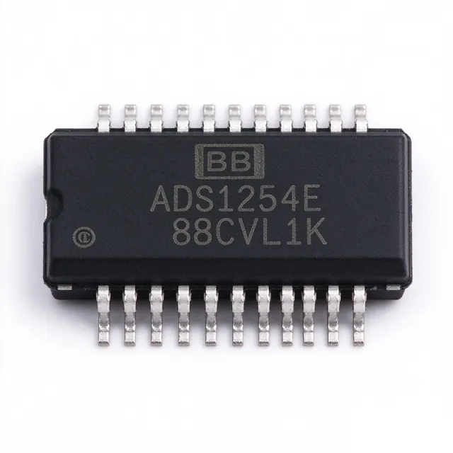
ADS1254E - 24-Bit 4-Channel 20-kSPS ADC | Texas Instruments
Texas Instruments ADS1254E is a 24-bit, 20-kSPS, four-channel delta-sigma analog-to-digital converter with separate AVDD and DVDD supplies, supplied in a 20-pin SSOP (DBQ) package. It provides four differential inputs, 19-bit effective resolution at 20 kSPS, low noise of 1.8 ppm, and maximum integral nonlinearity of 15 ppm. The converter supports an external reference, power-down operation, synchronization, and a low-power 20-kSPS operating mode. A delta-sigma ADC is a type of analog-to-digital converter that uses oversampling, digital filtering, and noise shaping to achieve high resolution and wide dynamic range. The ADS1254E belongs to the precision ADC hierarchy and is intended for industrial measurement systems requiring accurate conversion of low-bandwidth analog signals. Its differential inputs are suited to bridge sensors, strain-gauge measurements, and instrumentation-amplifier outputs. The principal features include a 24-bit conversion word without missing codes, four selectable differential input channels, and a maximum data rate of 20 kSPS. Effective resolution reaches 19 bits at that rate, while 1.8-ppm noise and 15-ppm maximum INL support precision measurements. Separate analog and digital supply domains help isolate sensitive analog circuitry from digital switching and interface loads. Internally, the device combines a precision delta-sigma conversion stage with programmable digital filtering and a synchronous serial interface. Synchronization permits coordinated sampling when multiple converters must acquire related analog signals. Power-down mode reduces consumption when measurements are not continuously required, while the low-power mode retains the stated 20-kSPS conversion capability. Typical applications include precision pressure and force measurement, industrial process monitoring, low-frequency data acquisition, laboratory instrumentation, and strain-gauge sensor interfaces. Four differential channels reduce the need for separate converter packages when several sensor outputs must be measured under common control. PCB design should keep analog input routing short, provide local bypass capacitance at AVDD and DVDD, and use a clean grounding strategy that minimizes converter digital-return current beneath sensitive analog traces. The external reference and input network must also be checked for thermal drift, settling time, and overdrive before choosing component values. This product page consolidates the verified manufacturer and distributor information, separates confirmed specifications from unavailable parameters, and provides practical guidance for evaluating the ADS1254E and its same-family drop-in alternatives.

ADS1254EG4 - 24-Bit 20-kSPS 4-Channel ADC | Texas Instruments
The Texas Instruments ADS1254EG4 is a 24-bit, four-channel, delta-sigma analog-to-digital converter rated for 20 kSPS conversion throughput and housed in a 20-pin SSOP package. It provides separate AVDD and DVDD supply connections, a flexible two-wire synchronous serial interface, and 19-bit effective resolution characterized by 1.8 ppm RMS noise. These characteristics position the ADS1254EG4 as a precision converter for industrial measurement, instrumentation, and low-frequency sensor acquisition systems. A delta-sigma ADC is a semiconductor data-conversion device that uses oversampling, digital filtering, and noise shaping to obtain high resolution from a relatively low-bandwidth signal chain. Within the converter hierarchy, the ADS1254EG4 belongs to the precision ADC category and uses a fourth-order sigma-delta modulator architecture. This method is particularly useful when measurement bandwidth is limited but input resolution and rejection of low-frequency noise are more important than very high sampling rates. The principal features include 24-bit nominal resolution, four single-ended input channels, a maximum conversion rate of 20 kSPS, and differential or single-ended analog input capability. Separate AVDD and DVDD pins allow the analog and digital portions of the circuit to use independently selected supply rails, helping reduce ground coupling between sensitive measurements and digital control signals. A programmable data rate, internal oscillator, and selectable input and reference voltages support adaptable measurement systems. The delta-sigma conversion architecture prioritizes narrow-band accuracy rather than waveform capture. Its digital decimation filter suppresses out-of-band noise, while the 19-bit effective resolution and 1.8 ppm RMS noise characterize the usable precision of the conversion chain. Because the input bandwidth is intentionally limited, applications must obey the datasheet's filter and settling requirements rather than treating the nominal 24-bit resolution as instantaneous across every possible input frequency. Typical uses include weighing systems, pressure and temperature measurement, laboratory instrumentation, process monitoring, and portable sensor interfaces. In each case, the device can acquire several low-frequency sensor channels through its serial interface while the host processor performs calibration, filtering, or unit conversion. The four-channel architecture also reduces the number of separate converters required when multiple slow-moving or multiplexed analog signals must be measured. PCB implementation should preserve the separation between analog inputs, the analog supply return, the digital interface, and the digital return path. Place the required input and decoupling capacitors close to their associated pins, use a quiet analog ground strategy, and route the serial clock and data lines away from sensitive analog nodes. Verify the selected data rate and digital filter settling time before using successive measurements in a control loop. This page combines manufacturer specifications, package and sourcing details, drop-in replacement analysis, application guidance, and design notes to support both component selection and board-level implementation. It is intended to help engineers evaluate the ADS1254EG4 against pin-compatible alternatives without overlooking the distinctions between resolution, conversion speed, filtering, interface behavior, and supply requirements.
ADS1255IDBR - 24-Bit 30kSPS Low-Noise ADC | Texas Instruments
The Texas Instruments ADS1255IDBR is a 24-bit, 30kSPS, very-low-noise delta-sigma analog-to-digital converter with two selectable inputs and a 20-SSOP package. It accepts differential or single-ended measurements through its flexible input multiplexer. The converter combines a fourth-order delta-sigma modulator with a programmable digital filter to support demanding precision instrumentation. A delta-sigma ADC is a voltage-regulating feedback modulator followed by digital filtering and decimation. It trades a relatively simple analog input stage for high resolution, strong noise suppression, and flexible conversion rates. The ADS1255 belongs to the ADC/DAC category within broader data-converter, signal-processing, and semiconductor hierarchies. Verified headline features include 24-bit resolution, no missing codes, a maximum output rate of 30kSPS, fast channel cycling, differential or single-ended input support, and programmable-gain operation. According to the Texas Instruments ADS1255 datasheet, every data-rate and PGA setting provides noise-free resolution to 23 bits. The published maximum nonlinearity is ±0.0010%. Technically, the fourth-order delta-sigma modulator shapes quantization noise away from the signal band, while the programmable digital filter removes that shaped noise and averages samples. A serial interface configures the converter and transfers conversion results. This architecture favors low-noise measurement rather than very high instantaneous throughput. Typical uses include precision pressure and load-cell front ends, industrial transmitters, laboratory instrumentation, temperature measurement, low-level sensor acquisition, and communication equipment. Differential input is valuable when sensor leads can pick up noise or when the source has meaningful common-mode variation. Design the analog front end around the selected PGA, reference voltage, input range, and desired data rate. Keep input and reference routing compact, decouple supply rails near the device, and provide a clean low-noise ground strategy. SSOP lead pitch also demands careful solderability and inspection planning. This page consolidates verified manufacturer information, distributor availability, procurement data, and engineering guidance. It also separates exact sourced facts from parameters requiring design confirmation instead of filling unsupported values with assumptions.

ADS1256IDBR - 24-Bit 30kSPS Delta-Sigma ADC | Texas Instruments
The Texas Instruments ADS1256IDBR is a 24-bit, 30kSPS, very-low-noise delta-sigma analog-to-digital converter with four differential and eight single-ended inputs, a programmable gain amplifier, and factory automation and process-control capability. It is supplied in a 28-pin SSOP package. The converter combines a fourth-order delta-sigma modulator with a programmable digital filter, enabling high-resolution measurement from low-frequency industrial sensors. A delta-sigma ADC is an analog-to-digital converter category that uses oversampling, noise shaping, and digital filtering to achieve high resolution. The ADS1256 belongs to the broader hierarchy of ADC, data-converter IC, signal-conditioning IC, and analog semiconductor devices. Its sigma-delta architecture is especially useful when high precision and noise performance matter more than very high bandwidth. The verified product information identifies a 24-bit conversion resolution, data rates up to 30kSPS, four differential or eight single-ended input choices, integrated PGA functionality, and a 28-SSOP package. These characteristics make the device suitable for precision current, voltage, resistance, and sensor measurements where the input bandwidth is limited. The manufacturer product page positions the device for factory automation and process control. The integrated PGA supports conditioning of low-level sensor outputs before conversion, while the programmable digital filter helps reject out-of-band noise. The four-wire serial interface supports digital control and data transfer, although signal timing, clocking, reference selection, and filter configuration must be implemented according to the manufacturer datasheet. The part is identified as a 28-SSOP device and is not a power semiconductor, so SOA data are not applicable. Typical applications include pressure and temperature measurement, industrial process monitoring, load-cell signal acquisition, laboratory instrumentation, and low-bandwidth sensor interfaces. The 30kSPS maximum data output rate is useful for many measurement loops, but it does not make the ADC suitable for high-frequency waveform acquisition. Input filtering, grounding, reference stability, and digital timing remain important for achieving predictable results. For PCB implementation, use a clean analog supply and ground structure, place input and reference components close to the converter, and keep digital communication traces away from sensitive analog nodes. Review the manufacturer datasheet for the exact pin names, recommended input network, reference requirements, and timing limits. This page combines the verified manufacturer and distributor information with application guidance and transparent data-gap markers. The main engineering tradeoff is that the ADS1256 prioritizes high-resolution, low-noise delta-sigma measurement over high-speed conversion. It is a strong fit for slow, precise industrial signals, but a different ADC architecture may be preferable when sampling many high-frequency points or handling substantially wider bandwidth.

ADS1258-EP - 16-Channel 24-Bit ADC | Texas Instruments
The ADS1258-EP is an enhanced product (EP) version of the ADS1258, a 16-channel (multiplexed), low-noise, 24-bit, delta-sigma (ΔΣ) analog-to-digital converter (ADC) from Texas Instruments. It provides single-cycle settled data at channel scan rates from 1.8k to 23.7k samples per second (SPS) per channel. The device operates from a unipolar 5-V or bipolar ±2.5-V analog supply and a digital supply compatible with interfaces ranging from 2.7 V to 5.25 V. It is available in QFN-48 and QFP-48 packages, specifically the 48-HTQFP (7x7) and 48-VQFN (7x7) variants. An analog-to-digital converter (ADC) is a device that converts continuous analog signals into discrete digital numbers. The ADS1258-EP is a high-resolution, multiplexed ADC designed for precision measurement applications. It belongs to the family of delta-sigma ADCs, which use oversampling and noise shaping to achieve high resolution. In the hierarchy of data converters, it sits under the category of analog-to-digital converters, which are essential in mixed-signal systems for interfacing real-world analog signals with digital processing. Key features of the ADS1258-EP include a flexible input multiplexer that accepts combinations of eight differential or 16 single-ended inputs, with a full-scale differential range of 5 V or true bipolar range of ±2.5 V. The device offers a 24-bit resolution with low noise, making it suitable for high-precision measurement. The enhanced product (EP) designation indicates a wider operating temperature range and higher reliability, as noted in TI's E2E forum. The ADS1258-EP is designed for applications requiring high accuracy and speed, such as industrial process control, medical instrumentation, and test and measurement equipment. Technically, the ADS1258-EP uses a delta-sigma modulator followed by a digital filter, achieving single-cycle settling, which is critical for multiplexed systems where each channel must be read quickly. The device includes an internal oscillator and a programmable gain amplifier (PGA) with gains of 1, 2, 4, 8, 16, 32, and 64, allowing direct connection to a variety of sensors. The digital interface is SPI-compatible, enabling easy integration with microcontrollers and DSPs. Typical applications include multi-channel data acquisition systems, industrial automation, medical monitoring, and precision instrumentation. The wide input range and high resolution make it ideal for measuring temperature, pressure, and strain gauge signals. The ADS1258-EP's enhanced temperature range (-55°C to +125°C) ensures reliable operation in harsh environments. When designing with the ADS1258-EP, ensure proper decoupling of the analog and digital supplies, and use a low-noise reference voltage. The multiplexer switching can cause settling issues; therefore, the single-cycle settling feature is essential. Also, consider the input impedance and use appropriate anti-aliasing filters to maintain accuracy.

ADS1262 - 32-Bit 38-kSPS Delta-Sigma ADC with PGA | TI
The Texas Instruments ADS1262 is a low-noise, low-drift, 38.4-kSPS, 32-bit delta-sigma analog-to-digital converter (ADC) with an integrated programmable gain amplifier (PGA), internal 2.5-V low-drift bandgap reference, and internal fault monitors, packaged in a 28-pin TSSOP and fully specified from -40C to +125C. A delta-sigma ADC is a type of ADC that uses oversampling and noise shaping to achieve very high resolution and low noise, making it the dominant architecture for precision sensor measurement. Within the signal-chain hierarchy, the ADS1262 functions as a complete analog front end (AFE): sensor -> PGA -> delta-sigma modulator -> digital filter -> SPI interface, replacing discrete amplifier-plus-ADC chains. Key features include 32-bit resolution, a maximum data rate of 38.4 kSPS, an integrated PGA with gains from 1 to 32, a 2.5-V internal reference with buffered output, and internal fault monitors for open and shorted sensor detection. A flexible input multiplexer supports 5 differential or 10 single-ended inputs, and the digital filter offers programmable data rates and filter modes for trading resolution against speed. A temperature sensor and GPIOs further reduce external component count and system cost. The device uses a chopper-stabilized delta-sigma modulator with a precision digital filter, delivering low drift and low offset without costly external auto-zero circuitry. Compared with the older ADS1256, the integrated reference removes the need for a precise external reference such as the REF5025, simplifying PCB layout. The integrated fault monitors continuously check sensor wiring, improving system reliability in industrial environments. Typical applications include weigh scales and load cells, RTD and thermocouple temperature measurement, and industrial process control front ends, where microvolt-level signals demand the ADS1262's resolution and noise performance. Price data from DigiKey and Mouser as of 2026-08-30. Design tip: power the analog supply from a clean 5-V LDO, bypass the reference with a 10-uF capacitor, and place decoupling close to the pins to realize the datasheet noise floor.

ADS1262IPW - 32-Bit 38-kSPS Delta-Sigma ADC | Texas Instruments (Tape & Reel)
The Texas Instruments ADS1262IPW is a 32-bit, 38.4-kSPS, low-noise delta-sigma (Sigma-Delta) analog-to-digital converter with an integrated programmable gain amplifier (PGA), voltage reference, and internal fault monitors, housed in a 28-pin TSSOP (PW) package. A delta-sigma ADC is a type of analog-to-digital converter that oversamples the input signal and applies digital filtering to achieve extremely high resolution, typically in the 24-bit to 32-bit class. Within the signal-chain hierarchy, the delta-sigma ADC sits between the analog front end (sensors, bridges) and the digital controller, and in this device the category is pushed further toward single-chip integration because the PGA and reference are built in, replacing several external precision components. Key features include 32-bit resolution with noise performance specified down to the nanovolt level at low data rates, an integrated PGA that amplifies small bridge and thermocouple signals directly, an on-chip low-drift voltage reference, and internal fault monitors for sensor diagnostics. The device is fully specified over the -40C to +125C industrial temperature range. Architecturally, the ADS1262 combines the delta-sigma modulator with programmable digital filtering, allowing trade-offs between output data rate (up to 38.4 kSPS) and noise. According to the TI ADS126x datasheet, the ADS1262 and ADS1263 family adds an auxiliary 24-bit delta-sigma ADC in the ADS1263 variant for background measurements, while both parts are pin and functionally compatible. Typical applications include weigh scales and load-cell front ends, factory automation and process-control analog inputs, and precision sensor measurement such as thermocouples and RTDs, where high accuracy and one-chip integration reduce board area and calibration effort. Design consideration: at the lowest data rates the device achieves its best noise floor, so select the output data rate and PGA gain together to match sensor sensitivity rather than defaulting to maximum speed. This page synthesizes distributor availability, drop-in family alternatives, and practical design guidance not consolidated in the manufacturer datasheet.
ADS1262IPWR - 32-Bit 38-kSPS Delta-Sigma ADC | Texas Instruments
The Texas Instruments ADS1262IPWR is a 32-bit, 38.4-kSPS, low-noise delta-sigma (Sigma-Delta) analog-to-digital converter with an integrated programmable gain amplifier (PGA), voltage reference, and internal fault monitors, housed in a 28-pin TSSOP (PW) package. A delta-sigma ADC is a type of analog-to-digital converter that oversamples the input signal and applies digital filtering to achieve extremely high resolution, typically in the 24-bit to 32-bit class. Within the signal-chain hierarchy, the delta-sigma ADC sits between the analog front end (sensors, bridges) and the digital controller, and in this device the category is pushed further toward single-chip integration because the PGA and reference are built in, replacing several external precision components. Key features include 32-bit resolution with noise performance specified down to the nanovolt level at low data rates, an integrated PGA that amplifies small bridge and thermocouple signals directly, an on-chip low-drift voltage reference, and internal fault monitors for sensor diagnostics. The device is fully specified over the -40C to +125C industrial temperature range. Architecturally, the ADS1262 combines the delta-sigma modulator with programmable digital filtering, allowing trade-offs between output data rate (up to 38.4 kSPS) and noise. According to the TI ADS126x datasheet, the ADS1262 and ADS1263 family adds an auxiliary 24-bit delta-sigma ADC in the ADS1263 variant for background measurements, while both parts are pin and functionally compatible. Typical applications include weigh scales and load-cell front ends, factory automation and process-control analog inputs, and precision sensor measurement such as thermocouples and RTDs, where high accuracy and one-chip integration reduce board area and calibration effort. Design consideration: at the lowest data rates the device achieves its best noise floor, so select the output data rate and PGA gain together to match sensor sensitivity rather than defaulting to maximum speed. This page synthesizes distributor availability, drop-in family alternatives, and practical design guidance not consolidated in the manufacturer datasheet.
ADS1263 - 32-Bit 38-kSPS Delta-Sigma ADC | Texas Instruments
The Texas Instruments ADS1263 is a low-noise, low-drift, 38.4-kSPS, 32-bit delta-sigma (ΔΣ) analog-to-digital converter with an integrated programmable gain amplifier (PGA) up to 32x, a 2.5V internal reference, and internal fault monitors. It is available in a 28-pin TSSOP package and is fully specified over the -40C to +125C temperature range. A key differentiator is its integrated auxiliary 24-bit ΔΣ ADC for background measurements, making it a complete, one-chip measurement solution for demanding sensor applications. A delta-sigma ADC is a type of analog-to-digital converter that uses oversampling and noise shaping to achieve very high resolution and excellent noise performance. Within the data converter hierarchy (ADC -> precision ADC -> delta-sigma ADC), the ADS1263 sits at the top precision tier, essential in data acquisition systems, sensor interfaces, and instrumentation. The integrated PGA and reference reduce external component count and simplify system design. Key features include 32-bit resolution, a maximum data rate of 38.4 kSPS, 5 differential or 10 single-ended input channels, PGA gains up to 32, and a 2.5V internal reference. The single-cycle settling digital filter provides 130-dB rejection of 50-Hz and 60-Hz line interference, ideal for weigh scales and load cells. The device also integrates IDAC excitation currents, an internal ADC test signal, and 8x multiplexed GPIO. Architecturally, the ADS1263 combines a delta-sigma modulator with a digital filter, delivering high resolution at low noise. The PGA connects directly to low-level sensor signals, while fault monitors (sensor burnout, supply, and reference monitoring) enhance system reliability. The auxiliary 24-bit ADC runs background measurements such as cold-junction temperature sensing without interrupting main conversions. Communication is via SPI in 4-wire or 3-wire modes. Typical applications include weigh scales, load cells, strain gauges, temperature sensing (RTD/thermocouple with IDACs), and precision industrial process control, where the low noise and integrated features reduce board space and design complexity. Design tip: decouple analog and digital supplies carefully, select PGA gain to match the sensor full-scale range to maximize dynamic range, and use the single-cycle settling filter for multiplexed channel scanning to eliminate filter settling wait states.
ADS1263IPW - 32-Bit Precision Delta-Sigma ADC | Texas Instruments
Texas Instruments ADS1263IPW is a 32-bit precision delta-sigma analog-to-digital converter with a 38 kSPS conversion rate, programmable gain amplifier, internal voltage reference, and auxiliary ADC in a 28-pin TSSOP package. It is designed for factory automation, industrial instrumentation, and sensor systems requiring high-resolution measurement from differential or single-ended inputs. A delta-sigma ADC is a category of data converter that uses oversampling, noise shaping, and digital filtering to achieve high resolution and excellent noise performance. The ADS1263 belongs to the ADC hierarchy, where it combines precision signal conditioning and conversion in one device. Its integrated PGA reduces the need for separate analog gain stages, while its reference and fault-monitor functions support sensor-ready measurement chains. The principal features include 32-bit resolution, a maximum conversion rate of 38 kSPS, and support for as many as 10 analog inputs. The device also includes an auxiliary 24-bit delta-sigma ADC for background measurements, allowing primary-channel and auxiliary measurements to share the same precision-converter family. A 5 V supply and operation from -40°C to +125°C support industrial temperature requirements. The low-noise, low-drift architecture is appropriate for slow but highly accurate sensor measurements. The programmable PGA can condition low-level bridge, thermocouple, strain-gauge, and pressure-sensor outputs before digitization. Integrated reference and internal fault-monitor functions help simplify system-level diagnostics, although the final accuracy of the complete measurement chain still depends on excitation, reference stability, input filtering, and PCB layout. Typical uses include weighing systems, factory sensors, pressure and temperature measurement, portable instrumentation, and multichannel data-acquisition systems. The auxiliary ADC can perform background diagnostics while the main ADC handles the primary measurement path, which is useful in systems that monitor sensor health or operating conditions without adding a separate low-speed converter. For PCB implementation, use a grounded analog plane beneath the converter, route the SPI interface away from sensitive analog inputs, place input and reference components close to their associated pins, and follow the manufacturer layout and grounding guidance. Verify the external reference arrangement, digital supply sequencing, and input common-mode limits before applying power. This page organizes the ADS1263IPW specifications, verified pricing context, same-package alternatives, application guidance, and design notes into an engineering-focused reference for evaluating and implementing this precision ADC.

ADS1271IPW - 24-Bit 105kSPS Delta-Sigma ADC | Texas Instruments | Industrial Measurement
The Texas Instruments ADS1271IPW is a 24-bit, single-channel sigma-delta analog-to-digital converter (ADC) with a maximum data rate of 105 kSPS, offered in a 16-pin TSSOP (PW) package and specified from -40 °C to +105 °C. It is designed for wide-bandwidth industrial measurement where both DC accuracy and AC performance across an extended temperature range matter. An ADC is the analog-to-digital converter, the device that turns a continuous voltage into a numeric code. The ADS1271 belongs to the delta-sigma (sigma-delta) sub-family: a high-order, chopper-stabilized modulator samples the input many times per output word, and an on-board decimation filter removes both modulator noise and out-of-band signal energy. Within the broader hierarchy, this part is a data-converter IC, that is, an integrated circuit in the interface IC class, sitting between a sensor or transducer and a digital processor. Key features include 24-bit resolution, a 105 kSPS maximum conversion rate, a single differential input channel, an SPI-compatible serial interface, and three selectable operating modes that let the designer trade speed against resolution and power. The chopper-stabilized modulator keeps drift low over the industrial temperature range, while the internal decimation filter suppresses out-of-band noise so external analog filtering can be minimized. A supply of approximately 4.75 V is indicated by the distributor part data. Technically, the ADS1271 combines a high-order modulator with an integrated FIR decimation filter and a chopper-stabilized front end. Three operating modes allow optimization of speed, resolution, and power dissipation, which lets a single design cover very different sampling needs. The result is an input stage usable directly with bridge sensors, thermocouple-style millivolt sources, and wide-dynamic-range industrial front ends without an external instrumentation amplifier. Typical applications include precision industrial process measurement, strain and load-cell bridges, vibration and condition monitoring, laboratory and test instrumentation, medical monitoring equipment, and low-rate high-resolution data acquisition such as temperature and pressure logging. A key design consideration is the decimation filter: the usable bandwidth and the noise performance are set by the selected operating mode, so the digital filter and averaging implemented in the host processor must match the data rate actually configured. Layout practice also matters for the differential input pair. This page consolidates the manufacturer datasheet and product-page parameters, distributor availability references, a parameter-by-parameter comparison against same-footprint TI converters, and practical design notes covering layout, filtering and pitfall avoidance that are not written out in the datasheet itself.

ADS1274IPAPT - 24-Bit 144kSPS Quad Delta-Sigma ADC | Texas Instruments
The Texas Instruments ADS1274IPAPT is a 24-bit, 4-channel, simultaneous-sampling delta-sigma analog-to-digital converter with data rates up to 144 kSPS per channel, housed in a 64-pin HTQFP (PAP) 10x10 mm package with exposed thermal pad. It delivers 111 dB SNR in high-resolution mode, -108 dB THD, and 62 kHz usable bandwidth, combining wideband audio performance with industrial-grade DC accuracy. The device features a chopper-stabilized modulator architecture that achieves very low offset drift of 0.8 uV/°C while maintaining flat passband response. A delta-sigma ADC is a type of oversampling converter that uses a high-frequency modulator followed by digital filtering to achieve very high resolution. The ADS1274 belongs to the wider category of precision ADCs, which sit in the signal chain hierarchy of analog front end -> analog-to-digital conversion -> digital processing. It is specifically optimized for applications that demand both wide bandwidth and excellent DC stability, two characteristics that are traditionally mutually exclusive in sigma-delta designs. Key features include four simultaneously-sampled differential inputs, selectable operating modes (High-Resolution, Low-Power, High-Speed, and Audio), a flexible serial interface (SPI-compatible or frame-sync), and an internal PLL for clock generation from an external reference. The wideband digital filter delivers low passband droop, eliminating the need for post-equalization in frequency-sensitive applications such as vibration analysis. Architecturally, the ADS1274 employs a 4th-order chopper-stabilized modulator per channel with proprietary decimation filtering. This design eliminates the traditional trade-off between DC precision (low drift, high DC CMRR) and AC performance (wide bandwidth, flat passband), making the part suitable for multisensor systems where each channel must accurately capture both static and dynamic signals without per-channel calibration. Typical applications include industrial vibration monitoring, condition monitoring of rotating machinery, seismic data acquisition, multi-channel data loggers, audio test equipment, and power-quality analyzers. The simultaneous sampling architecture preserves phase relationships between channels, which is critical for modal analysis in structural health monitoring. When designing with the ADS1274IPAPT, pay attention to PCB layout: the exposed thermal pad must be soldered to a ground plane with multiple thermal vias to dissipate heat from the digital core, and the analog supply (AVDD) should be heavily decoupled with separate 10 uF bulk and 100 nF ceramic capacitors close to the pin. Use a low-jitter master clock for best noise performance at maximum data rate. This page synthesizes distributor pricing, parametric comparison tables, drop-in alternatives, and practical design notes not found on the standalone TI datasheet, helping engineers shorten the selection and qualification cycle for high-channel-count precision acquisition systems.

ADS127L11 - 24-Bit 400-kSPS Delta-Sigma ADC | Texas Instruments
The ADS127L11 is a 24-bit, delta-sigma (ΔΣ), analog-to-digital converter (ADC) from Texas Instruments, offering data rates up to 400 kSPS with the wideband filter and up to 1067 kSPS with the low-latency filter. It combines excellent AC performance and DC precision with low power consumption of 18.6 mW in high-speed mode. The device integrates input and reference buffers to reduce signal loading and simplify front-end design. Available in a 20-pin TSSOP package (IPWR) and a 20-pin VQFN package (IRUKR), it operates over a wide supply range and is suitable for industrial, medical, and test and measurement applications. A delta-sigma ADC is a type of analog-to-digital converter that uses oversampling and noise shaping to achieve high resolution (typically 16 to 32 bits) with relatively low cost and power. It is part of the ADC family, which converts continuous analog signals into discrete digital values. Delta-sigma ADCs are widely used in precision measurement, audio, and industrial control where high resolution and low noise are critical. They differ from SAR ADCs in that they trade speed for resolution and often include digital filters for anti-aliasing. Key features of the ADS127L11 include a programmable digital filter (wideband or low-latency), a 24-bit resolution, and a maximum sample rate of 1067 kSPS. The device supports both SPI and frame-sync serial interfaces, and includes an internal reference buffer and input buffer. It offers a signal-to-noise ratio (SNR) of [DATA_NEEDED: SNR] dB and a total harmonic distortion (THD) of [DATA_NEEDED: THD] dB. The power consumption is 18.6 mW in high-speed mode, making it suitable for battery-powered and portable instruments. Technically, the ADS127L11 uses a fourth-order delta-sigma modulator with a digital decimation filter. The wideband filter provides a passband up to 0.45 × data rate, while the low-latency filter offers faster settling for multiplexed applications. The device includes a reference buffer that allows the use of external references with high impedance, and an input buffer that reduces the kickback from the switched-capacitor input stage. The ADC operates from a single 3.3V or 5V supply, with a digital I/O supply from 1.8V to 3.6V. Typical applications include vibration monitoring, industrial process control, medical instrumentation (e.g., EEG, ECG), and high-precision data acquisition systems. The high data rate and low latency make it ideal for closed-loop control and real-time monitoring. The integrated buffers simplify the analog front-end, reducing component count and board space. When designing with the ADS127L11, ensure proper decoupling of the AVDD and DVDD supplies, and use a low-noise reference. The input buffer requires a bias voltage, and the reference buffer should be bypassed with a capacitor. For best performance, keep the analog input traces short and shielded from digital noise.

ADS1281IPW - 31-Bit 4-kSPS Seismic ADC | Texas Instruments
Texas Instruments ADS1281IPW is an ultra-high-resolution, single-channel delta-sigma analog-to-digital converter designed for seismic and energy-exploration instrumentation. It converts one differential input at up to 4 kSPS, provides a 31-bit conversion result, and is packaged in a 24-pin TSSOP. The device integrates the analog front end, fourth-order inherently stable delta-sigma modulator, digital filter, and serial interface into one compact converter. A delta-sigma ADC is a voltage-sampling data-converter category that uses continuous-time modulation and digital noise shaping to obtain high resolution from low-speed measurements. In the broader electronics hierarchy, the ADS1281 belongs to the ADC family, then to delta-sigma converters, then to integrated data-converter ICs and semiconductors. Its architecture is especially appropriate for slow, high-precision measurements where narrow-band noise and integrated digital filtering are more important than high conversion throughput. The ADS1281's principal characteristics include one differential analog input, a maximum conversion rate of 4 kSPS, a 31-bit output resolution, and a fourth-order inherently stable modulator. A differential input supports rejection of common-mode noise when the source is balanced. The integrated digital filtering reduces the bandwidth of high-frequency noise before the conversion result is delivered, while the low-noise converter architecture helps preserve weak signals in geophone or other high-impedance sensing systems. Technically, the ADS1281 combines a fourth-order delta-sigma modulation stage with integrated filtering and a serial data interface. Because delta-sigma conversion trades conversion speed for resolution and noise shaping, it is better suited to vibration, seismic, energy-metering, and precision instrumentation signals than to high-bandwidth waveform conversion. The single-chip architecture reduces board area by consolidating the signal-conditioning and conversion functions, but careful analog grounding, reference design, supply bypassing, and digital-interface layout remain essential. Typical uses include seismic acquisition systems, vibration monitors, energy-exploration equipment, precision weighing, geophone interfaces, and industrial instrumentation with narrow-band sensor signals. Its differential input can simplify the connection of bridge-style or balanced sensors, while the digital filter supports measurements where slow-changing sensor information must be isolated from environmental noise. For PCB design, keep the analog input, reference, and supply paths compact and route digital clock and data traces away from sensitive sensor nodes. Use the application information in the TI datasheet for the recommended input and reference network. Confirm the selected external resistor, capacitor, and clock values against the operating mode because filter settings and digital decimation affect conversion latency. This product overview combines the device architecture, package details, practical use cases, and sourcing guidance to support design review. The comparison and selection notes emphasize the difference between true pin-compatible replacements and converters that merely share a similar resolution or package, preventing a footprint match from being mistaken for functional equivalence.

ADS1286P - 12-Bit 20kHz Micropower ADC | Texas Instruments
Texas Instruments ADS1286P is a 12-bit, 20kHz micropower sampling analog-to-digital converter with a differential input, sample-and-hold amplifier, and 250 uA supply current. The device uses an SPI- or SSI-compatible serial interface over a two-wire or three-wire connection and is packaged in an 8-pin PDIP. It is intended for low-power signal acquisition where compact conversion, differential input handling, and low supply demand are important. A sampling ADC belongs to the analog-to-digital converter hierarchy, which converts continuous analog voltages into digital data for measurement, control, and communication systems. The ADS1286P combines a successive-approximation-style sampling architecture with an integrated sample-and-hold stage. Its differential input can measure the voltage difference between two analog nodes, which helps reject common-mode interference when paired with suitable input filtering and reference design. The 12-bit conversion resolution provides 4096 digital codes, while the 20kHz sampling rate supports acquisition of relatively high-frequency analog signals. Low 250 uA supply-current demand makes the converter appropriate for battery-operated instruments, portable monitoring equipment, and remote sensor nodes. Its serial interface reduces the number of signal lines required between the converter and a host controller. The internal sample-and-hold amplifier acquires the differential input before conversion, simplifying the front-end signal path. Because accuracy and noise performance depend on reference and input conditioning, designers should follow the manufacturer datasheet when selecting external resistance, capacitance, grounding, and digital-interface arrangements. The serial interface supports SPI-compatible and SSI-compatible communication, allowing the device to be connected to microcontrollers, serial peripherals, and embedded control systems. Typical applications include portable medical instruments, industrial pressure and temperature monitoring, low-power environmental sensors, battery-powered data loggers, and precision process-control nodes. Differential inputs are especially useful when the measured signal is small relative to environmental noise. System partitioning should preserve the converter's differential-input architecture rather than converting the signal into a single-ended path unnecessarily. PCB design should keep analog input traces short, place filtering components close to the converter, and maintain a quiet return path for the analog and digital grounds. The manufacturer datasheet should be used to assign every pin and to select bypass capacitors because the supplied technical summary does not reproduce the complete electrical-characteristics table or pin-description table. This page organizes the device's core function, verified operating characteristics, package details, applications, and design considerations into an engineering-focused reference. It also distinguishes true same-footprint alternatives from family members offered in different packages, helping designers avoid replacements that require PCB changes.
ADS1286PA - 12-Bit, 37 kSPS Low-Power ADC | Texas Instruments
The Texas Instruments ADS1286PA is a 12-bit, single-input SAR analog-to-digital converter with a 37 kS/s conversion rate, differential input, and 250 µA nominal supply current in an 8-PDIP package. It operates from a 4.5 V to 5.25 V single supply and combines a sample-and-hold amplifier with an SPI or SSI-compatible serial interface for compact, low-power measurement systems. An ADC is an analog-to-digital converter, a semiconductor that samples a continuous voltage and converts it into a digital code for processing. The ADS1286 belongs to the sampling ADC and SAR ADC hierarchy, where successive approximation rounds the input voltage during each conversion. Its differential architecture measures the voltage between two analog inputs, improving rejection of common-mode interference when the signal source is balanced. Key characteristics include 12-bit resolution, a 37 kS/s conversion rate, and a nominal supply current of 250 µA. The converter offers 90 dB of spurious-free dynamic range, 1 LSB differential nonlinearity, and 2 LSB integral nonlinearity. Its SPI and SSI-compatible serial interface supports two-wire or three-wire communication, reducing the number of connections required in remote and distributed sensing equipment. The sampling architecture captures the analog input before conversion, while the internal sample-and-hold amplifier isolates the source during successive approximation. Differential input handling is useful for bridge sensors, instrumentation signals, and other systems in which common-mode noise can obscure a low-level signal. The 8-PDIP package is suitable for through-hole prototyping, educational instruments, and legacy industrial control systems where a surface-mount footprint is unnecessary. Typical applications include battery-powered portable instruments, pressure and temperature monitoring, industrial sensor interfaces, laboratory measurement equipment, and low-power remote data-acquisition nodes. The 250 µA nominal current and 4.5 V to 5.25 V supply range are particularly useful when system power is constrained and a regulated 5 V rail is already available. When designing around the ADS1286PA, preserve the input voltage range, provide a stable reference, and route the differential input pair symmetrically to minimize pickup from nearby switching circuitry. Input filtering, reference bypassing, and a quiet grounding strategy are central to achieving the converter's specified linearity and dynamic-range performance. This page organizes the principal electrical specifications, application guidance, package information, and verified substitute constraints for ADS1286PA. It also distinguishes true pin-compatible replacements from related devices that require a different footprint, helping engineers shorten component-selection and board-layout work without overlooking package-level compatibility.
ADS1286PAG4 - 12-bit 20kHz Micro Power SAR ADC | Texas Instruments
The Texas Instruments ADS1286PAG4 is a 12-bit, 20 kHz sampling analog-to-digital converter (ADC) with a differential input and integrated sample-and-hold amplifier that consumes only 250 µA of supply current. Housed in an 8-pin plastic DIP (PDIP-8) package, it operates from a single +5 V analog supply and communicates over an SPI/SSI-compatible two- or three-wire serial interface. The G4 designator indicates the device ships in tube packaging and is lead-free Pb-free, RoHS-compliant. An SAR (Successive Approximation Register) ADC is a type of Nyquist-rate data converter that uses a binary-weighted capacitor array and a comparator to converge on the analog input voltage in N clock cycles, where N is the resolution in bits. SAR ADCs occupy the middle ground between slow high-precision delta-sigma converters and flash ADCs; they deliver low latency (one conversion per cycle), deterministic throughput suitable for multiplexed acquisition, and modest power draw. The ADS1286PAG4 belongs to the broader hierarchy: ADC -> data converter -> data acquisition IC -> signal chain -> mixed-signal semiconductor. Key features include a guaranteed-no-missing-codes 12-bit transfer function, a 20 kHz maximum sampling rate, a 60 µs typical conversion time, only 250 µA of supply current during continuous conversion, and a low 0.0488 % linearity error (1 LSB). The differential input stage rejects common-mode noise on long analog runs, and the synchronous serial output minimizes MCU pin count. Operating temperature spans -40 °C to +85 °C, qualifying it for industrial-grade chassis-mount and remote-instrumentation designs. Architecturally, the ADS1286PAG4 combines a precision CMOS capacitor-DAC successive-approximation core with an on-chip clock and reference input path. Designers feed the reference from a stable 5 V rail (or an external low-drift reference) and digitize true-differential or single-ended bipolar signals up to ±VREF. The serial data frame is MSB-first, allowing direct hand-off to microcontrollers, FPGAs, or DSPs without glue logic. Typical applications include portable instrumentation, remote battery-powered data loggers, industrial process-control analog front ends, hand-held multimeters, and transducer/sensor signal conditioning where low power and small PCB area are required. Choose the ADS1286PAG4 when you need 12-bit precision at moderate speed from a single 5 V rail with deterministic conversion latency. Design tip: place the 0.1 µF supply bypass capacitor within 5 mm of the VDD pin and route the differential analog traces as a tightly-coupled pair to maximize common-mode rejection. The ADS1286PAG4 is pin-compatible with several 8-pin PDIP ADC descendants from the same TI family, simplifying PCB reuse across product variants.
ADS1286PC - 12-Bit 20kHz Micropower SAR ADC | Texas Instruments
The Texas Instruments ADS1286PC is a 12-bit, 20 kHz micropower sampling analog-to-digital converter with one differential input, a sample-and-hold amplifier, and an 8-pin PDIP package. It consumes only 250 µA of supply current and supports SPI- and SSI-compatible serial communication over two-wire or three-wire interfaces. A sampling ADC is an analog-to-digital converter that acquires an input voltage with a sample-and-hold circuit before conversion. The ADS1286 belongs to the ADC, data converter, and signal-processing semiconductor hierarchy. Its differential input allows a sensor output to be measured relative to a reference node, which can improve rejection of common-mode noise when the signal source, analog ground, and digital return paths are designed carefully. The converter provides 12-bit resolution and a maximum sampling rate of 20 kSPS. A differential input, integrated sample-and-hold amplifier, and low 250 µA supply current make the device suitable for compact, battery-powered measurement systems. The serial interface supports SPI and SSI-compatible operation, allowing the ADC to communicate with microcontrollers and other digital controllers over a small number of signal lines. The ADS1286 uses a successive-approximation-register conversion architecture. This approach supports a compact implementation and efficient conversion timing while avoiding the higher power and complexity commonly associated with continuously operating high-speed conversion architectures. Its two-wire or three-wire serial interface reduces board-routing requirements, which is valuable where connector pins, PCB area, and standby power are constrained. Typical applications include remote sensor acquisition, industrial process measurement, portable instrumentation, battery-operated data loggers, and low-power embedded monitoring systems. The ADS1286 is particularly appropriate when measurements must be captured locally and transferred through a serial interface rather than through a parallel data bus. The 250 µA supply-current characteristic also helps limit average system energy when the converter is operated intermittently. Designers should follow the manufacturer datasheet for analog input range, reference voltage, acquisition timing, bypass-capacitor values, and digital-interface timing. Input and reference grounds should be kept quiet, and the serial clock should be driven only while data is required if the host processor cannot shut down its output pins between conversions. This page combines the manufacturer device description, ordering information, package details, interface characteristics, drop-in replacement findings, and practical selection guidance to support faster engineering decisions for the ADS1286PC 12-bit micropower sampling ADC.
ADS1286PK - 12-Bit Micropower SAR ADC | Texas Instruments
The Texas Instruments ADS1286PK is a 12-bit, 20 kHz micropower sampling analog-to-digital converter with a differential input, an integrated sample-and-hold amplifier, and a supply current of 250 µA in an 8-pin PDIP package. The converter uses successive-approximation conversion and provides a single analog input channel suitable for precision, low-power signal acquisition. An ADC is an interface component that converts an analog voltage into a digital number for processing by a microcontroller, DSP, logger, or measurement instrument. The ADS1286 belongs to the sampling ADC hierarchy, which includes sample-and-hold front ends, differential analog inputs, and serial-output converters. Its differential architecture is useful when the measurement must reject common-mode noise or when the source is balanced and centered around a reference level. The ADS1286 provides 12-bit resolution, a maximum sampling rate of 20 kHz, and typical supply current of 250 µA. These characteristics make it suitable for low-power instrumentation where the converter must acquire sensor information while consuming little system energy. The serial interface is compatible with SPI and SSI protocols and supports communication over a two-wire or three-wire arrangement, allowing the device to operate with limited connector pins. Internally, the ADS1286 combines a differential input, sampling circuitry, a 12-bit successive-approximation converter, and a serial interface in one package. The differential input is conditioned by the integrated sample-and-hold amplifier before conversion. Serial data output reduces the number of signal connections required, while the compact PDIP-8 package supports conventional through-hole PCB assembly and prototype rework. The exact reference-voltage, input-range, timing, and dynamic-performance details should be confirmed in the manufacturer datasheet before final circuit design. Typical uses include portable environmental monitoring, remote sensing, industrial process measurement, low-power battery instrumentation, and small laboratory data loggers. A differential sensor such as a bridge, thermocouple interface, or current-sense element can feed the converter when its common-mode range and source impedance meet the device requirements. The 20 kHz sampling capability also permits measurement of slowly varying analog quantities without requiring a high-speed converter. Power-supply and reference design remain central to achieving useful accuracy. Decoupling capacitors should be placed close to the supply pins, and analog and digital return currents should be routed without sharing narrow paths with the input signal. The input source impedance must be checked against the sampling network, while the reference voltage determines the conversion scale and must remain within its permitted operating range. This page combines the manufacturer specifications, a structured pin-compatible substitute review, comparison parameters, application guidance, and practical layout considerations for engineers evaluating the ADS1286PK. The supporting information distinguishes confirmed device characteristics from parameters that still require datasheet confirmation during component selection and circuit sign-off.
ADS1286PL - 12-Bit 20kHz Micropower ADC | Texas Instruments
Texas Instruments ADS1286PL is a 12-bit, 20kSPS micropower sampling analog-to-digital converter with one differential input, a sample-and-hold amplifier, and an 8-pin PDIP package. It operates from a 5V supply and consumes only 250uA of supply current, combining low conversion rate with compact, low-power signal acquisition for industrial, medical, and remote sensor systems. A sampling ADC is a successive-approximation-register, or SAR, converter that acquires an analog voltage with a sample-and-hold circuit and converts it through successive bit decisions. The ADS1286 belongs to the ADC hierarchy within data-converter and signal-chain semiconductors. Its differential input accepts two related analog signals and converts their voltage difference, helping reject common-mode noise when the source is arranged as a bridge, sensor, or instrumentation amplifier. The device provides 12-bit conversion resolution, a 20kSPS conversion rate, and a serial interface compatible with SPI and SSI protocols. The interface uses either a two-wire or three-wire arrangement described in the manufacturer datasheet. Low 250uA supply consumption is the defining micropower feature, making the converter suitable for battery-operated and remotely powered equipment where each milliampere can influence the enclosure size or service interval. The ADS1286 uses a sample-and-hold amplifier ahead of the SAR conversion core. The analog input is sampled during the acquisition interval, after which the internal successive-approximation network resolves the sampled voltage to 12 bits. Serial data transfer reduces the number of interconnects required compared with a parallel ADC, although it also makes the host interface timing and signal-integrity design important in systems operating at higher clock rates. Typical uses include low-frequency pressure and temperature acquisition, low-current battery monitoring, industrial panel controls, portable medical instrumentation, and remote sensor nodes. The 20kSPS rate is appropriate for many slow or medium-bandwidth physical measurements, while the 250uA supply current favors low-duty-cycle acquisition. Differential operation is especially useful when the measured signal is small relative to environmental offsets. Designers should follow the manufacturer datasheet for input-range, reference, clock, and interface details. Keep analog and digital return paths separated, place input and reference bypass capacitors close to their pins, and account for source impedance during acquisition. The 8-pin PDIP package is through-hole and suits prototypes, legacy industrial equipment, and hand-assembled or leaded-production designs where a surface-mount footprint would be undesirable.

ADS1286U - 12-Bit 20kHz Micro Power ADC | Texas Instruments
The Texas Instruments ADS1286U is a 12-bit, 20 kHz micro-power sampling analog-to-digital converter (ADC) with a differential input, integrated sample-and-hold amplifier, and a high-speed SPI/SSI-compatible serial interface, housed in an 8-pin SOIC package. The device draws only 250 uA of supply current, operates from a single 4.5 V to 5.25 V supply, and guarantees no missing codes across the full temperature range. An analog-to-digital converter is a mixed-signal integrated circuit that converts a continuous-time, continuous-amplitude analog signal into a discrete digital code. The ADS1286 belongs to the successive-approximation-register (SAR) ADC product family within the broader signal-chain taxonomy that includes sigma-delta, pipeline, and flash converters. SAR ADCs are favored for low-power, single-shot, and multiplexed data-acquisition tasks because they offer deterministic latency, compact silicon area, and inherently low power consumption compared with higher-resolution delta-sigma parts. Key specifications of the ADS1286U include 12-bit resolution, a 20 kHz maximum sampling rate, an integral non-linearity of +/-1 LSB (max), and a SINAD of 72 dB. The differential input stage accepts a +/-Vref full-scale range (typically 0 V to 5 V single- or 5 V differentially) and is preceded by a sample-and-hold that eliminates the need for an external front-end amplifier in most applications. The serial interface is clock-synchronized and supports two- or three-wire operation with an external serial clock rate up to 4 MHz, easing isolation between the converter and the host microcontroller. Architecturally, the ADS1286 uses a charge-redistribution SAR core with a thin-film laser-trimmed input scaling network; this topology yields the very low 250 uA quiescent current while preserving 12-bit DC accuracy. The internal reference loop is designed for use with an external 2.5 V or 5 V reference, and the device does not include an on-chip reference. The wide-input-range CMOS input structure simplifies sensor-bridge and thermocouple front ends. Typical end-use applications for the ADS1286U include battery-powered instrumentation, remote data loggers, isolated industrial sensors, portable medical devices, and handheld meters. Its tiny 8-pin SOIC footprint and 250 uA supply current make it especially attractive for loop-powered 4-20 mA transmitters and other energy-harvested nodes where every microamp matters. A practical design consideration is the addition of an anti-aliasing RC filter ahead of the analog inputs: a 1 kohm/10 nF single-pole filter is sufficient for a 20 kHz Nyquist boundary. Decouple VDD with a 0.1 uF ceramic placed within 5 mm of the supply pin. This page synthesizes distributor pricing, verified drop-in alternatives, and practical layout notes not found on generic catalog summaries.
ADS1286U/2K5G4 - 12-Bit 20kHz Micropower SAR ADC | TI
The Texas Instruments ADS1286U/2K5G4 is a 12-bit, 20 kHz successive-approximation analog-to-digital converter (SAR ADC) with a differential input and integrated sample-and-hold amplifier, packaged in an 8-pin SOIC (0.154", 3.90 mm width) and consuming only 250 µA of supply current. It supports a single-ended or differential analog input over a 0 V to 5.3 V range and a 5 V nominal supply, providing SPI/SSI-compatible two- or three-wire serial communication for microcontroller, FPGA, or DSP hosts. This micropower combination of low supply current and a 20 kSPS sample rate makes it well suited to battery-powered and isolated data-acquisition front ends. A successive-approximation ADC (often abbreviated SAR ADC) is a type of data-conversion IC that walks an internal capacitive DAC from MSB to LSB each conversion cycle, producing a low-latency, deterministic sample output with no pipeline delay. SAR ADCs are widely used when a system needs a clean single-shot sample with simple control, low standby current, and modest resolution - they sit between slower sigma-delta ADCs (which trade latency for higher resolution) and flash ADCs (which trade power for speed). Within a system, the SAR ADC is positioned just after analog signal conditioning and ahead of a digital controller that consumes the conversion result. Key features include guaranteed no missing codes at 12 bits, 20 kHz maximum sampling rate, 250 µA typical supply current, an SPI/SSI-compatible serial interface, a single 5 V supply, and an industrial -40 °C to +85 °C operating temperature range. The 8-SOIC footprint and two-wire serial interface simplify board layout and reduce MCU pin overhead in space-constrained designs. The architecture combines an input sample-and-hold with a charge-redistribution SAR core and a precision internal reference path, giving deterministic latency of one conversion cycle and the absence of pipeline or integration delay. Because the digital interface is a simple shift-register readout, the part is straightforward to drive from virtually any microcontroller with an SPI peripheral. Typical applications include remote sensor data acquisition, isolated analog front ends, battery-powered instrumentation, industrial process-control transducers, and portable medical accessory boards. The DIP and SOIC footprints also support hand-soldered prototype or through-hole-style retrofit boards. When designing the analog front end, take care to bypass VDD with a 0.1 µF ceramic close to the pin and to keep the analog input traces short and guarded, since the 12-bit, 20 kSPS converter will expose any added noise or reference drift directly in the conversion result. This page consolidates distributor pricing, pin-compatible drop-in alternatives, and practical design guidance not found in the standalone manufacturer datasheet.