DC-DC Converters
بەرهەمەکان (770+)

TDA38826XUMA1 - 20A Synchronous Buck Regulator, 2.7-16V | Infineon
The Infineon TDA38826XUMA1 is a 20 A fully integrated, highly efficient synchronous DC-DC buck regulator housed in a 21-pin PowerUFQFN (QFN-21) package. It accepts an input voltage range of 2.7 V to 16 V (with an external bias supply supporting the upper end) and produces an adjustable output from 0.9 V up to roughly 5.5 V, making it well-suited for point-of-load conversion in computing and telecom hardware. The device uses a fast Constant On-Time (COT) control architecture that simplifies loop compensation while delivering sub-microsecond transient response to load steps. A 20 A continuous output current rating, integrated high-side and low-side MOSFETs, and 38-page datasheet (Rev 2.0, July 2023) define its core capability envelope. Per the Infineon datasheet, the standard pack quantity is 3000 units on tape and reel, and the orderable part number TDA38826XUMA1 identifies the reeled variant of the base TDA38826 die. A buck regulator (step-down switching converter) is a type of switched-mode power supply (SMPS) that uses an inductor and synchronous FET switches to convert a higher DC input voltage to a lower DC output voltage at high efficiency. Within the power management hierarchy, the buck converter sits between the linear regulator (low noise but inefficient at high step-down ratios) and the isolated converter (used for offline or safety-isolated rails). COT (Constant On-Time) control is a variant of hysteretic control in which the high-side switch is turned on for a fixed time each switching cycle, with the off-time determined by the output voltage crossing a feedback threshold; this yields fast transient response without requiring complex Type-II/III compensation networks. Key differentiating features of the TDA38826 include integrated MOSFETs (eliminating external switch selection), COT control (removing compensation engineering effort), 20 A continuous output current, adjustable output from 0.9 V, and a wide 2.7 V to 16 V input range with external bias. Infineon's IPOL (Integrated Point-of-Load) family targets server, telecom, and graphics-rack power rails where density and design simplicity outweigh the need for ultra-low-noise linear regulation. The COT control loop uses the output ripple to trigger switching events, achieving fast load-step response without external compensation components. This architecture is robust to ceramic output capacitor ESR variation and supports pre-biased startup, a useful feature when powering FPGAs or ASICs that already have residual charge on their rails at hot-plug events. Typical applications include 12 V-to-POL conversion for server core rails, ASIC/FPGA core and memory supplies, datacom and telecom cards, and graphics-card voltage rails. The wide input range also accepts 5 V or 3.3 V intermediate bus voltages in distributed power architectures. When designing with this regulator, place input capacitors as close as possible to the VIN and PGND pins to minimize switching-node parasitic inductance. A 2 x 22 µF ceramic input capacitor bank is typical for 20 A operation, and the output filter inductor should be sized to keep peak-to-peak ripple current below 30% of the load for best transient behavior. This page synthesizes Infineon datasheet specifications, distributor pricing, and drop-in alternative guidance for engineers evaluating the TDA38826XUMA1 against competing IPOL and DC-DC point-of-load parts.
TDA38827AUMA1 - 25A OptiMOS IPOL Buck Regulator | Infineon
The Infineon TDA38827AUMA1 is a fully integrated 25 A single-voltage synchronous buck regulator housed in a 22-pin PowerVQFN package. It combines an onboard PWM controller with Infineon OptiMOS 5 power MOSFETs (including integrated bootstrap diode), delivering adjustable output from 0.6 V up to a high current in a compact footprint. The part uses a fast constant on-time (COT) control scheme that simplifies the design effort and achieves fast control response for demanding point-of-load (POL) applications. A buck regulator is a switch-mode DC-DC converter that steps a higher input voltage down to a lower regulated output voltage with high efficiency. Within the power management hierarchy, a buck converter belongs to the broader family of switching regulators, which sit alongside linear regulators (LDOs) and charge pumps in the DC-DC converter category. Integrated POL (point-of-load) regulators such as the TDA38827 incorporate the controller, FETs, and often bootstrap drive into one IC, eliminating external MOSFETs and shrinking board area versus discrete buck designs. Key specifications include 25 A continuous output current, 0.6 V minimum adjustable output, constant on-time (COT) control for fast transient response, and integrated OptiMOS 5 FETs with built-in bootstrap diode. The COT architecture provides pseudo-fixed switching frequency, near-unity duty ratio operation at heavy load, and inherently stable output without external compensation network. The 22-pin PowerVQFN package (PG-IQFN-22) exposes a thermal pad that conducts heat from the integrated MOSFETs to the PCB copper pour. Typical applications include server and datacom POL rails, telecom card voltage rails, distributed bus converters in storage and networking hardware, FPGA/DSP core and I/O supplies, and high-current ASIC power delivery. The combination of 25 A capability and a compact package suits space-constrained boards where designers need high current density and reduced BOM count. When designing with this part, follow Infineon's recommended input/output capacitor values and observe the thermal pad layout guidelines. The COT control scheme depends on the output ripple for stable switching, so external ripple injection or a low-ESR output capacitor network may be required in some configurations.

TEA1721AT/N1 - 700V Flyback SMPS Controller, 5W | NXP
The NXP Semiconductors TEA1721AT/N1 is a compact, low-cost Switched Mode Power Supply (SMPS) controller IC with integrated 700V power MOSFET for low-power flyback converters up to 5W, housed in a 7-pin SO (SOT1175-1 / SOIC-7) package. The device operates directly from a rectified universal mains input (up to 700V drain rating), supports a switching frequency of 22.5 kHz to 50.5 kHz, and delivers ultra-low standby power consumption via a burst-mode frequency of 430 Hz. A flyback controller is a type of switched-mode power supply (SMPS) topology that stores energy in the primary-side transformer's magnetic field during the MOSFET on-time and releases it to the secondary winding during the off-time, providing galvanic isolation between mains and low-voltage outputs. The TEA1721AT/N1 belongs to the AC-DC controller category within the broader Power Management IC hierarchy and is designed for isolated, non-isolated, and auxiliary power supply applications where eliminating external high-voltage startup components is critical. Key features include a 700V integrated power switch, 22.5 kHz to 50.5 kHz programmable switching frequency, 430 Hz burst-mode frequency for ultra-low standby power, valley and demag detection for quasi-resonant operation, and comprehensive protection circuitry including over-temperature, over-current, and short-winding protection. The integrated high-voltage startup eliminates the need for an external startup resistor network, reducing BOM count and PCB footprint. The TEA1721AT/N1's high-voltage integration and quasi-resonant valley switching architecture maximize efficiency across the entire load range. The internal MOSFET supports universal mains input (85 VAC to 265 VAC) without auxiliary high-voltage components, simplifying layout and reducing standby power to industry-leading levels required for ENERGY STAR and EU Ecodesign compliance. Typical applications include 5W mobile phone chargers, standby power supplies for white goods and appliance control, IoT and smart home low-power modules, and auxiliary supplies for larger power systems.

TEA2017AAT/3 - Digital LLC + Multimode PFC Combo Controller | NXP
The NXP Semiconductors TEA2017AAT/3 is a digital configurable LLC and multimode PFC combo controller for high-efficiency resonant power supplies, integrating both the LLC controller and PFC controller functionality in a compact 16-pin SO (SO16) package, supporting applications from 90 W to 1000 W. An LLC + PFC combo controller is a power management IC that governs the two main power-conversion stages of a modern AC-DC supply: the power factor correction (PFC) front end and the LLC resonant half-bridge stage that provides isolated, regulated DC output. Within the power management IC hierarchy, it belongs to AC-DC controllers with integrated PFC, where combining both control loops in a single IC reduces component count, board area, and design complexity. Key features include a fully digital architecture built on a high-speed configurable hardware state machine ensuring reliable real-time performance, a PFC configurable for DCM/QR or CCM fixed-frequency operation, and integrated advanced functions such as active X-capacitor discharge and external OTP (over-temperature protection) sensing. The PFC control uses average current mode, delivering low input-current distortion and high power factor across the universal AC input range. Technical depth: because both control engines share one digital die, inter-stage coordination such as burst-mode operation at light load and PFC/LLC sequencing is handled natively, enabling very high efficiency from light load to full 1000 W output. Paired with the TEA2095T dual-channel LLC resonant synchronous rectifier controller, the TEA2017AAT forms a complete high-performance, cost-effective resonant power supply solution. Typical applications include server and telecom power supplies, LED street lighting drivers, audio amplifiers, notebook and desktop adapters, and open-frame industrial power supplies in the 90 W to 1000 W range. Design consideration: according to NXP, the TEA2017AAT/3 is a pin-compatible update of the TEA2017AAT/2, but a few small differences must be considered when replacing /2 with /3; for new designs the /3 version is preferred. Route the PFC current-sense network close to IC pin 4 GND near the PFC sense resistor and bulk capacitor ground. This page synthesizes distributor pricing, drop-in alternatives verified against NXP application note AN13140, and practical design notes not found in the manufacturer datasheet.
TEA2017ABT/2 - LLC + DCM/QR PFC Combo Controller | NXP
The NXP TEA2017ABT/2 is a digital configurable LLC and DCM/QR PFC combo controller IC for high-efficiency resonant power supplies, integrating an LLC controller and a PFC controller that operates in DCM/QR mode, housed in a low-profile, narrow-body 16-pin SO16 (SOIC 3.90 mm width) surface-mount package. A combo controller is a power management IC that merges two control functions on a single die: the power factor correction (PFC) stage, which shapes the AC input current to achieve near-unity power factor, and the LLC resonant converter stage, which provides isolated, high-efficiency DC conversion via a resonant tank. Within the power supply controller hierarchy, the TEA2017ABT belongs to the AC-DC controller family, sitting above discrete PWM controllers and below full digital power supervisory systems. Combo integration reduces board area, simplifies inter-controller handshake logic, and lowers the total component count of the complete resonant power supply. Key features include a digital architecture based on a high-speed configurable hardware state machine, which ensures very reliable real-time control performance without the latency or software-dependency of a microcontroller-based design. The PFC stage supports DCM (discontinuous conduction mode) and QR (quasi-resonant) operation only, while the LLC stage is identical to that of the TEA2017AAT variant. During power supply development, many operation and protection settings of both the LLC and PFC controllers are digitally configurable, giving designers flexibility typically reserved for digital power platforms. Technically, the state-machine-based digital architecture executes cycle-by-cycle control decisions deterministically, supporting valley switching, adaptive dead time, and multi-mode protection handling. Because the LLC engine and the PFC engine are coordinated on-chip, burst-mode operation and shutdown sequencing can be tightly coupled, improving light-load efficiency. Typical applications include AC-DC adapters for notebooks and high-power chargers, open-frame and enclosed industrial power supplies, and LED lighting drivers where high efficiency, low standby power, and a low component count are required. When designing with the TEA2017ABT, note that the PFC operates only in DCM/QR mode: for applications demanding continuous conduction mode PFC at higher power levels, evaluate the TEA2017AAT variant instead. This page synthesizes verified distributor pricing, drop-in family alternatives, and practical design notes not found in the manufacturer datasheet.

TEA2095T - GreenChip Dual LLC Synchronous Rectifier Controller | NXP
The NXP Semiconductors TEA2095T is a GreenChip dual synchronous rectifier (SR) controller IC for switched-mode power supplies, dedicated to secondary-side synchronous rectification in resonant (LLC) converters with center-tapped transformer outputs, housed in an 8-pin SO (SOIC-8) package with two integrated gate-driver stages. A synchronous rectifier controller replaces the lossy output rectifier diodes of an SMPS with MOSFETs that are actively gate-driven, drastically cutting conduction losses. In a center-tapped LLC converter, two SR MOSFETs alternately rectify the two half-cycles; a dual SR controller such as the TEA2095T senses the drain voltages of both MOSFETs and drives the correct gate at the correct time. This device family sits in the NXP secondary-side AC-DC controller hierarchy under power management ICs and is part of the GreenChip energy-efficiency portfolio. The defining feature of the TEA2095T is its adaptive gate drive method. Instead of a fixed minimum on-time, the controller continuously adapts the gate-drive window to the actual conduction interval of each SR MOSFET, maximizing energy savings at any load. This prevents both premature turn-off (body-diode conduction losses) and late turn-off (cross-conduction and reverse-current risks), which are the two classic failure modes of synchronous rectification in resonant converters. The TEA2095T provides two driver stages, one per SR MOSFET, with direct drain sensing on the DSA and DSB pins. NXP documentation notes an interlock delay time with a typical value of 200 ns, which guarantees non-overlap between the two gate outputs even under transient conditions, protecting the SR MOSFETs from shoot-through. Internal circuitry connected to the DSA and DSB pins should not be polluted with series resistors, as NXP's application guidance explains that added resistance can degrade the adaptive-drive regulation through voltage offset. Typical applications include LLC resonant converters in adapters and chargers for notebooks, high-power USB-PD chargers, LED driver power supplies, server and telecom auxiliary power stages, and TV power boards, wherever high efficiency across light and full load is mandated by energy regulations such as CoC and DoE. A key design consideration: when migrating from the older TEA1795T, note that the DSA/DSB inputs behave differently, and the NXP community guidance warns that series resistors on these pins can degrade regulation; a PCB review is advised. This page adds distributor sourcing context, drop-in alternative analysis, and practical design notes synthesized beyond the manufacturer datasheet for engineering and procurement teams.
TEA2095T-1-S30J - Dual LLC SR Controller, 38V | NXP
The NXP Semiconductors TEA2095T/1/S30J is a high-performance GreenChip dual synchronous rectifier (SR) controller IC for switch-mode power supplies, operating from a 4.75 V to 38 V supply with a typical supply current of 90 uA, housed in an 8-pin SOIC (0.154 inch, 3.90 mm width) surface-mount package. A synchronous rectifier controller is a specialized power management IC that replaces the output rectifier diodes of a switched-mode power supply with actively driven MOSFETs. Because a MOSFET channel exhibits a far lower voltage drop than a Schottky or fast-recovery diode, SR controllers dramatically reduce conduction losses and raise overall conversion efficiency. In the power-supply hierarchy, the TEA2095T belongs to the family of secondary-side power conversion controllers used alongside LLC resonant converters and other resonant topologies. The TEA2095T incorporates NXP's adaptive gate drive method, which evaluates the conduction state of the SR MOSFETs cycle by cycle and adjusts gate-drive timing to save the maximum amount of energy at any load. Its two integrated driver stages are dedicated to driving the SR MOSFETs that rectify the outputs of a center-tapped transformer secondary, which is the standard configuration for low-voltage, high-current LLC resonant converters. Architecturally, the device is a dedicated controller for synchronous rectification on the secondary side of resonant converters. The adaptive algorithm extends SR operation down to light load, where conventional fixed-timing SR controllers would turn the MOSFETs off prematurely, and it guards against reverse current at low load, improving both full-load efficiency and light-load standby power - key requirements of modern energy-efficiency regulations such as those addressed by NXP's GreenChip portfolio. Typical applications include the secondary side of LLC resonant converters in notebook adapters, server and telecom power supplies, LED TV power boards, and high-density USB-PD fast chargers, wherever a center-tapped secondary with low-output-voltage, high-output-current rectification demands minimal conduction loss. A key design consideration is correct placement and routing of the SR sense signals; because the controller drives two MOSFETs synchronously with the resonant half-cycle, layout symmetry between the two drive channels and short, low-inductance gate loops are essential to avoid spurious turn-on and to preserve the efficiency benefit at 100 kHz-class resonant frequencies. This page adds value beyond the manufacturer datasheet by synthesizing distributor pricing, availability, drop-in alternatives, and practical engineering design notes in one place. According to the NXP TEA2095T product page and distributor listings, pricing starts at approximately $1.0833 (as of 2026-09-13, LCSC), and the part is actively stocked.

TEA2208T/1 - Active Bridge Rectifier Controller | NXP
The NXP Semiconductors TEA2208T/1 is a full-wave active bridge rectifier controller that replaces the traditional diode bridge with low-ohmic high-voltage external MOSFETs, delivered in a 14-pin SOIC package. An active bridge rectifier controller is a power management IC that drives four external MOSFETs in an H-bridge configuration so that AC mains is rectified with conduction losses far below those of a conventional 4-diode bridge. In the power-conversion hierarchy it sits at the input stage of an AC-DC converter, ahead of the main switching stage, and directly determines end-to-end efficiency of desktop PC power supplies and notebook adapters. Key features include high-current rail-to-rail MOS output drivers that minimize driver dissipation and gate-charge losses to as low as 2 mW combined, elimination of rectifier diode forward-conduction losses, and a silicon-on-insulator (SOI) process for high-voltage robustness. According to NXP product data, converter efficiency improves by up to about 1.4% at 90 V AC mains input - a significant gain in high-volume, energy-regulated applications. Technically, the TEA2208T senses AC line polarity and sequences the four gate drivers so that only the diagonal MOSFET pair conducts in each half cycle. Because the external MOSFETs are selected by the designer, conduction loss scales with RDS(on) rather than a fixed diode Vf, allowing efficiency optimization across a wide power range. The SOI process isolates high-voltage domains on chip, supporting direct interfacing with the rectifier node. Typical applications include desktop and notebook PC power supplies, server and adapter AC-DC front ends, and high-density power converters subject to 80 PLUS and similar efficiency regulations. Design-wise, select external MOSFETs with low RDS(on) and adequate VDS rating for the applied mains; the controller itself dissipates very little, but MOSFET choice determines total rectifier loss. This page synthesizes distributor pricing, drop-in alternatives, and practical design notes not found in the manufacturer datasheet.
TEA2226AT/1 - Digital Configurable LLC Resonant Controller | NXP
The NXP Semiconductors TEA2226AT/1 is a digital configurable controller for high-efficiency resonant (LLC) power supplies, delivered in a 16-pin SO (SOIC) surface-mount package. It integrates a high-voltage silicon-on-insulator (SOI) controller for high-voltage start-up, integrated gate drivers, a level shifter, protection circuitry, and circuitry that ensures zero-voltage switching (ZVS). A resonant LLC controller is a type of switched-mode power-supply (SMPS) control IC that drives a half-bridge resonant converter operating at or near the resonant frequency of an LC tank. Within the power management hierarchy (AC-DC controller -> resonant converter controller -> power management IC), LLC topologies enable very high efficiency and low electromagnetic interference because switches toggle under zero-voltage switching conditions, minimizing switching losses. Key features of the TEA2226AT include fully digital configurability, which dramatically reduces external component count and simplifies power-supply design; integrated high-voltage start-up circuitry that removes the need for a separate auxiliary low-power start-up supply; built-in drivers and level shifting for the high-side and low-side bridge switches; and comprehensive protection functions. According to NXP, supplies built on this controller meet efficiency regulations including Energy Star, the US Department of Energy (DoE), the EU Eco-design directive, and the European Code of Conduct. The digital architecture allows designers to configure operating parameters in firmware or via configuration rather than hard-wired analog networks, enabling one controller platform to serve multiple power levels and output configurations. This shortens design cycles and supports platform strategies across product families. Typical applications include high-efficiency AC-DC adapters and power supplies for consumer electronics, audio power amplifiers, servers and set-top boxes, and industrial auxiliary supplies where efficiency regulations drive topology choice. The TEA2226AT is commonly paired with an upstream PFC controller such as the NXP TEA2376DT in two-stage designs. When designing with this controller, verify start-up behavior with the integrated high-voltage SOI stage and observe NXP application guidance for burst-mode operation at light load to maximize standby efficiency. This page synthesizes distributor availability, alternatives context, and practical design notes not found in the manufacturer datasheet, providing added selection value beyond raw specification listings.
TEA2226AT/1Y - Digital Configurable LLC Controller | NXP
The NXP Semiconductors TEA2226AT/1Y is a digital configurable LLC resonant converter controller for high-efficiency AC-DC power supplies, housed in a 16-pin SOIC (SO16) package with a supply voltage window of 18.2 V to 19.7 V. An LLC controller governs a resonant half-bridge topology in which two MOSFET switches drive a series resonant tank (inductor-capacitor-inductor) through a transformer. By modulating the switching frequency, the controller regulates the output while the tank naturally achieves zero-voltage switching (ZVS), dramatically cutting switching losses compared with conventional hard-switched PWM converters. LLC controllers sit at the heart of the power management IC hierarchy, above generic PWM controllers and alongside PFC controllers in complete AC-DC solutions. Key features of the TEA2226AT include a digital configurable architecture that enables power supply design with a very low component count, integrated gate drivers, and an internal level shifter for the high-side switch. The device contains a high-voltage silicon-on-insulator (SOI) controller stage for direct high-voltage start-up, eliminating the need for an auxiliary low-power startup supply. On-chip circuitry ensures zero-voltage switching under normal operation, and a suite of integrated protections guards the converter against fault conditions. Architecturally, the TEA2226AT combines digital configurability with the robustness of an SOI high-voltage process. Digital configuration allows the resonant control behavior to be tailored to the application without extensive external analog component tuning, shortening design cycles and improving consistency between units. Typical applications include notebook and desktop adapter power supplies, server and telecom rectifier stages, and consumer electronics adapters that must meet Energy Star, US Department of Energy (DoE), European Union Ecodesign, and European Code of Conduct efficiency regulations. Design-wise, verify that the SUPHS floating supply for the high-side driver stays within the 18.2 V to 19.7 V window, and follow the NXP datasheet guidance for bootstrap and protection component selection. This page synthesizes distributor availability data, the manufacturer datasheet, and practical design notes not found on the standard distributor product pages.
TEA2376DT - Digital Interleaved PFC Controller | NXP
The NXP Semiconductors TEA2376DT is a digital configurable two-phase interleaved PFC (power factor correction) controller for high-efficiency AC-DC power supplies, operating in discontinuous conduction mode (DCM) or quasi-resonant (QR) mode with valley switching at 25 kHz to 300 kHz, housed in a 14-pin SO-14 (SOIC-14) surface-mount package. A PFC controller is a power management IC that shapes the input current waveform of a switch-mode power supply so that it follows the input voltage, raising the power factor toward unity and reducing harmonic distortion. Within the power-supply control hierarchy - AC-DC converter, PFC pre-stage, PWM main converter - the PFC controller governs the boost converter front end and is essential for meeting international mains harmonics requirements in equipment above roughly 75 W. Key features of the TEA2376DT include digital configurability that reduces external component count, two-phase interleaved operation that halves input ripple current and spreads thermal stress across two boost switches, valley switching that minimizes MOSFET turn-on losses, and phase shedding with burst mode for high efficiency at light load. Technically, the device runs a digitally controlled regulation loop that can be tuned through configuration, supporting both discontinuous and transition conduction modes across a 25 kHz to 300 kHz switching range. NXP documents typical system power levels up to 1000 W, noting that high switching frequency and high power applications require attention to IC package thermal limits. The companion TEA2209T is used for the main converter stage in reference designs such as the 1 kW TEA2376DB1623 evaluation board. Typical applications include TV power supplies, computing and server power supplies, and industrial AC-DC power systems where efficiency standards such as 80 PLUS class targets and low standby power drive the architecture. When designing with the TEA2376DT, verify thermal dissipation of the SO-14 package at the target switching frequency and output power, and configure phase shedding thresholds to maximize light-load efficiency without audible noise. This page synthesizes distributor data, the NXP datasheet, drop-in alternatives, and practical design notes not found in the manufacturer datasheet alone.
TEA2376DT-1Y - Interleaved PFC Controller, 25-300kHz | NXP
The NXP Semiconductors TEA2376DT/1Y is a digital configurable two-phase interleaved PFC (power factor correction) controller for high-efficiency AC-DC power supplies, operating in discontinuous conduction mode (DCM) or quasi-resonant (QR) mode with valley switching, across a 25 kHz to 300 kHz switching-frequency range, housed in a 14-pin SO (SO14) surface-mount package. A PFC controller is a power management IC that shapes the input current waveform of an AC-DC converter to follow the input voltage, achieving a high power factor and low harmonic distortion as required by IEC harmonics regulations in modern off-line power supplies. Interleaved two-phase topologies split the PFC power stage into two parallel, phase-shifted branches, halving input ripple current and easing EMI filter design. Key features of the TEA2376DT include digital configurability via a high-speed configurable hardware state machine, which ensures reliable real-time control without firmware; valley switching in QR mode to reduce switching losses; and integrated protections such as cycle-by-cycle current limiting and overvoltage protection for robust operation. Under light load, the controller supports phase shedding, in which one interleaved phase is disabled, combined with burst mode operation to maintain high efficiency down to very low output power - a key requirement for energy-efficiency standards in TVs, computing and server PSUs. Typical applications include television power supplies, desktop PC and server power supplies, and industrial AC-DC systems. NXP's TEA2376DB1623 reference design demonstrates a 1 kW standalone two-phase interleaved PFC using the TEA2376DT paired with the TEA2209T X-capacitor discharge controller. Design consideration: with a two-phase interleaved stage, careful PCB layout balancing both phase current loops and routing the two gate-drive outputs symmetrically is essential to guarantee equal current sharing between phases. This page adds value beyond the manufacturer datasheet by synthesizing distributor pricing and stock data, drop-in family alternatives, and practical engineering notes in one place.
TEA6017AT/1 - Digital LLC + Multimode PFC Controller | NXP
The NXP Semiconductors TEA6017AT/1 is a digital configurable LLC and multimode PFC combo controller for high-efficiency resonant power supplies, covering a 50 kHz to 200 kHz switching range and integrating both LLC and PFC controller functionality in a single low-profile, narrow-body SO16 package. A PFC (power factor correction) controller shapes the input current of an AC-DC power supply so that it follows the input voltage waveform, minimizing harmonic distortion and meeting regulatory requirements such as IEC harmonic limits. In the broader power-management hierarchy, it sits within the class of power supply control ICs and power controllers. The TEA6017AT/1 combines this PFC function with an LLC resonant converter controller, the topology of choice for high-efficiency, low-EMI isolated DC-DC stages in modern AC-DC supplies. Key features include PFC operability in DCM/QR, CCM fixed-frequency, or multimode operation, allowing designers to optimize efficiency across the entire load range. The digital architecture is based on a high-speed configurable hardware state machine, delivering very reliable real-time performance without firmware. Complete resonant power supply functionality is achieved with a very low external component count, reducing BOM cost and board area. Technically, the device is the industrial-market equivalent of the TEA2017AAT with improved driver performance, improved ESD performance, and enhanced reliability, per NXP product information. The hardware state machine implements protection and control timing deterministically, which simplifies compliance-focused designs. Applications include notebook adapters, USB-PD fast chargers, TV power supplies, and industrial AC-DC systems where high efficiency and low standby power are mandatory. A key design consideration is configuring the PFC mode (DCM/QR, CCM, or multimode) to match the target power level and efficiency curve; multimode operation yields the best light-load efficiency. Ensure adequate creepage and gate-drive layout discipline around the LLC and PFC driver outputs. This page synthesizes distributor pricing, verified drop-in alternatives, design notes, and parameter comparisons not found in the manufacturer datasheet.
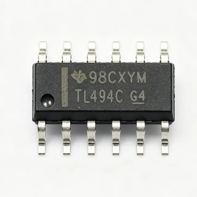
TL494CDT - PWM Controller IC | STMicroelectronics | SMPS
The TL494CDT is a fixed-frequency pulse-width modulation (PWM) control circuit from STMicroelectronics, designed primarily for switch-mode power supplies (SMPS). It integrates all the functions required for a single-ended or push-pull switching power supply, including an internal oscillator, error amplifiers, a 5V reference, and output control logic. The device operates from a supply voltage of 7V to 40V and is available in a 16-pin SOIC (SOP-16) package, making it suitable for compact power supply designs. A PWM controller is a specialized integrated circuit that generates a variable-duty-cycle square wave to regulate the output voltage of a switching power supply. It compares a feedback signal to a reference voltage and adjusts the duty cycle of the output transistors accordingly. The TL494 belongs to the family of voltage-mode PWM controllers, which are widely used in offline and DC-DC converters due to their simplicity and robustness. This category sits within the broader hierarchy of power management ICs, which also includes linear regulators, switching regulators, and battery management devices. Key features of the TL494CDT include a complete PWM power-control circuitry, an uncommitted output for single-ended or push-pull operation, an internal oscillator with a frequency range of 1kHz to 300kHz, and a 5V reference with 5% tolerance. It also provides an error amplifier with a common-mode voltage range of -0.3V to VCC-2V, a dead-time control comparator, and a standby current of typically 6mA. These features enable precise regulation and protection in various power conversion topologies. The TL494CDT uses a bipolar process technology, offering a proven and reliable architecture that has been in production for decades. It includes an internal 5V reference that can source up to 10mA for external use, and its output stage can sink or source up to 250mA. The device also features a shutdown control pin that can be used for overcurrent or overvoltage protection, and its dead-time control allows adjustment of the minimum off-time to prevent transformer saturation in push-pull designs. Typical applications include switch-mode power supplies for computers, telecom equipment, industrial systems, and battery chargers. The TL494CDT is also used in DC-DC converters, inverters, and motor control circuits. Its wide supply voltage range and flexible output configuration make it a versatile choice for both single-ended and push-pull topologies. When designing with the TL494CDT, it is important to properly set the oscillator frequency using external timing components (RT and CT) and to ensure adequate decoupling of the VCC pin. The dead-time control pin should be used to prevent shoot-through in push-pull stages, and the error amplifier compensation network must be designed for stable loop operation. This page synthesizes distributor pricing, drop-in alternatives, and practical design notes not found in the STMicroelectronics datasheet, providing a comprehensive resource for engineers selecting a PWM controller for their power supply design.

TL594INSR - 40V 0.2A 300kHz PWM Controller | Texas Instruments
The Texas Instruments TL594INSR is a 40 V, 0.2 A, 300 kHz pulse-width-modulation (PWM) controller with integrated undervoltage lockout (UVLO), housed in a 16-pin Small-Outline (SOP/NS) package supplied on tape and reel. The device integrates a precision reference, two error amplifiers, an adjustable oscillator, a dead-time control comparator, and uncommitted output transistors capable of sinking or sourcing up to 200 mA each for driving power stages directly. What is a PWM controller? A PWM controller is a power-management integrated circuit that generates switching signals whose duty cycle is modulated to regulate voltage or current in switching power supplies. The TL594 belongs to the voltage-mode PWM controller category, which sits in the hierarchy of PWM controller -> switching controller -> DC-DC controller -> power management IC -> semiconductor. Voltage-mode controllers regulate by comparing an error-amplifier output to a sawtooth waveform, making them robust, well-understood, and tolerant of noisy measurement environments. The TL594INSR supports buck, boost, flyback, forward, full-bridge, half-bridge, and push-pull topologies, giving designers a single IC for multiple converter architectures. Key features include 5 V (±5%) internal reference output, programmable dead-time control (DTC), programmable oscillator frequency up to 300 kHz via external RT and CT, and uncommitted 200 mA open-collector outputs that can be configured in common-emitter or emitter-follower mode for either single-ended or push-pull operation. At the architecture level, the TL594 uses a bandgap-derived 5 V reference feeding two identical error amplifiers with uncommitted inputs and outputs, allowing flexible feedback loop design. The oscillator section generates a sawtooth whose rise time is set by RT-CT and whose maximum frequency is 300 kHz, with internal circuitry that prevents simultaneous conduction of the output stages during transitions (dead-time control). Protection features include UVLO with typical 6 V turn-on threshold and thermal considerations for the SOP-16 (NS) thermal pad. Typical applications include DC-DC converters in industrial power systems, SMPS for telecom and networking equipment, battery chargers using buck or boost topologies, and motor-drive forward converters. Designers favor the TL594 for its topology flexibility and proven architecture in long-lifecycle designs. When designing with this part, ensure RT and CT values are selected to keep oscillator frequency below 300 kHz under all temperature and tolerance conditions, and add adequate bulk capacitance on VCC to prevent UVLO retriggering during start-up.

TLE8366EVXUMA1 - 1.8A 45V Step-Down DC/DC | Infineon
The Infineon TLE8366EVXUMA1 is a 1.8 A PWM step-down DC/DC converter with integrated high-side power switch, packaged in a small PG-DSO-8 (Exposed Pad) with 0.6 V to 16 V adjustable output from a 4.75 V to 45 V input. It belongs to Infineon's automotive-grade OPTIREG power management family and is offered in three variants: fixed 5.0 V (TLE8366EV50), fixed 3.3 V (TLE8366EV33), and adjustable 0.6 V to 16 V output (TLE8366EV, this part). The exposed thermal pad PG-DSO-8 (3.90 mm body width) provides low thermal resistance for sustained 1.8 A operation. A buck converter (also called step-down switching regulator) is a switched-mode power supply topology that uses an inductor, a synchronous or asynchronous switch, and a control loop to convert a higher DC input voltage into a lower, well-regulated DC output voltage with efficiencies typically above 90 %. Within the power management hierarchy, the TLE8366 sits between a high-voltage battery or bus rail and downstream point-of-load regulators, providing an isolated, regulated intermediate rail for analog, microcontroller, or sensor subsystems. Key features of this variant include 4.75 V to 45 V wide input range (suitable for 12 V and 24 V automotive buses with load-dump transients), adjustable output from 0.6 V to 16 V via external resistor divider, integrated 1.8 A power switch, PWM current-mode control, cycle-by-cycle current limiting, over-temperature shutdown, input undervoltage lockout, and an enable pin that drops quiescent current below 2 µA in shutdown. The switching frequency is fixed, allowing predictable EMI filter design. The TLE8366 uses current-mode control with internal slope compensation, providing excellent line and load transient response. The exposed thermal pad allows direct PCB heat-sinking, supporting continuous 1.8 A output across the automotive -40 °C to +150 °C junction temperature range with proper board layout. Typical applications include automotive ECUs, body control modules, instrument clusters, HVAC controllers, sensor power supplies, industrial 24 V bus systems, and any point-of-load regulation downstream of a noisy or wide-ranging input rail. The wide input voltage range also makes it suitable for battery-powered equipment with deeply discharged cells. When designing with this device, choose the inductor, output capacitor, and bootstrap capacitor per the manufacturer datasheet's reference design values. Place the input ceramic capacitor as close as possible to the VIN and PGND pins to minimize switching-node ringing, and use sufficient copper area on the exposed pad for thermal dissipation at maximum load. This page synthesizes Infineon product-page data, distributor pricing, parametric cross-references, and practical design considerations to give engineers a single, citable reference that complements the manufacturer datasheet.
TLE83862ELXUMA1 - 700kHz Boost Controller, 4.75-45V Input | Infineon
The Infineon TLE83862ELXUMA1 (die: TLE8386-2EL) is an automotive-grade, low-side-sense boost controller with built-in protection features, packaged in a 14-pin PG-SSOP-14-EP (exposed pad) outline. It operates from a 4.75 V to 45 V input range, drives an external N-channel MOSFET in a step-up (boost) topology, and supports an adjustable switching frequency from 100 kHz to 700 kHz that can be synchronized to an external clock source. A boost controller is a DC-DC switching controller that regulates an output voltage higher than the input by cycling an external power inductor through a low-side switch. The TLE83862ELXUMA1 belongs to the Infineon TLE8386 family of automotive-grade boost controllers, positioned within the broader power management IC hierarchy as a switching controller -> DC-DC controller -> voltage regulator -> power management IC -> semiconductor. Key features include 700 kHz adjustable switching frequency, 4.75 V to 45 V wide input range, low-side current sensing for simplified ground-referenced feedback, external synchronization capability, integrated protection such as overcurrent, overvoltage, and thermal shutdown, and AEC-Q100 automotive qualification. The exposed thermal pad on the PG-SSOP-14-EP package supports efficient heat removal from the controller IC, which is critical when operating at the upper end of the input range. The TLE83862ELXUMA1 uses a peak-current-mode control architecture with a low-side shunt resistor for current sensing, enabling cycle-by-cycle overcurrent protection and good transient response. The switching frequency is set by a single resistor at the RT pin, providing flexibility to optimize efficiency versus component size. The device integrates a high-side gate driver capable of driving logic-level N-channel MOSFETs in boost configurations for input voltages up to 45 V. Typical applications include automotive LED headlight boost converters, pre-boost supplies for downstream buck regulators in 12 V / 24 V automotive systems, USB-PD / Type-C adapter power stages, industrial 24 V to higher voltage rails, and battery-backed boost converters. The AEC-Q100 qualification makes it especially suited for harsh automotive environments subject to load-dump and cold-crank transients. When designing with this part, ensure the input capacitor is sized to handle the pulsating current of the boost topology, and route the low-side current-sense traces as a Kelvin connection to the shunt resistor to preserve current-mode control accuracy. The exposed pad must be soldered to a sufficiently large copper pour to keep junction temperature within the -40 C to +125 C operating range during load-dump events. This page synthesizes distributor pricing, drop-in alternatives from the Infineon TLE8386 family, application circuits, and practical PCB layout notes that go beyond the manufacturer datasheet.
TLF51801ELVXUMA1 - 10A Synchronous Buck Controller, 45V, AEC-Q100 | Infineon
The Infineon TLF51801ELVXUMA1 is a 10 A synchronous PWM step-down DC/DC controller with external n/n-MOSFET drivers, packaged in a 14-pin PG-SSOP with exposed thermal pad. It operates from 4.75 V to 45 V input, supports a 99% maximum duty cycle, and is rated for -40 C to +150 C junction temperature with AEC-Q100 automotive qualification. A PWM step-down (buck) controller is a type of switching voltage regulator that uses external MOSFETs as the power switches, a controller IC to drive those switches, and an LC output filter to deliver a lower regulated output voltage. Within the broader power-management hierarchy, the buck controller sits above integrated buck converters (which embed the switches) and below point-of-load regulators; it is chosen when load current exceeds integrated-converter capability, here up to 10 A, while still requiring controller-grade flexibility for switching frequency, current sense, and protection thresholds. Key features include a 700 kHz nominal switching frequency, adjustable current limit via R_DS(on) sensing on the high-side switch, integrated bootstrap gate drive for the high-side n-MOSFET, and a 99% duty cycle that enables low-dropout operation near the input rail. The controller uses voltage-mode control with an external compensation network and includes an enable input, power-good output, and soft-start capability. The architecture is built on a bipolar / BiCMOS process with a precision internal reference, allowing tight load and line regulation across the automotive temperature range. Synchronous rectification eliminates the need for an external Schottky diode at high-side, raising efficiency at high load currents and reducing thermal stress in compact modules. Typical applications include automotive body and chassis ECUs, LED driver front-ends, industrial 24 V sensor and actuator rails, and any point-of-load conversion above 3 A that demands automotive-grade reliability and wide input-voltage tolerance. A 45 V abs-max input allows operation directly from 12 V and 24 V automotive buses with substantial transient margin. When designing with this controller, select external MOSFETs with adequate safe-operating-area margin at worst-case VIN = 45 V and programmed peak current; the PG-SSOP-14 EP package dissipates gate-drive losses but the high-side / low-side FETs carry switching loss, so thermal design of the FETs is the dominant concern, not the IC itself. This page synthesizes distributor pricing, AEC-Q100 qualification status, drop-in same-package alternatives, and practical design notes that complement, rather than duplicate, the manufacturer datasheet.
TLS4125D0EPV50XUMA1 - 2.5A 5V AEC-Q100 Buck Converter | Infineon
The Infineon TLS4125D0EPV50XUMA1 is an OPTIREG Switcher synchronous step-down (buck) DC/DC converter delivering a fixed 5V output at up to 2.5A from a wide 3.7V to 40V automotive input bus, housed in a 14-pin TSDSO (PowerTSSOP, 3.90mm width) exposed-pad package. Key specifications include a 2.8 MHz nominal switching frequency, ±1.5% PWM-mode feedback accuracy, 34 µA quiescent current, integrated power MOSFETs, and configurable 320 kHz to 560 kHz or 1.6 MHz to 2.8 MHz operating ranges. The IC supports PFM light-load mode for high efficiency at low current, synchronization input, spread spectrum modulation, and an integrated reset function with adjustable undervoltage/overvoltage thresholds. A buck converter is a switched-mode DC/DC topology that steps a higher DC input voltage down to a lower regulated DC output by alternately storing energy in an inductor and releasing it to a load through synchronous MOSFETs. The TLS4125D0EPV50XUMA1 belongs to the broader hierarchy of switching regulators -> DC/DC converters -> power management ICs -> semiconductors, and within Infineon's portfolio it sits in the OPTIREG automotive-grade family targeted at ECU point-of-load rails. Architecturally, the device integrates high-side and low-side MOSFETs, internal compensation, a soft-start circuit, and a precision feedback loop that holds 5V ±2% across line, load, and temperature variations. Spread spectrum and synchronization help meet CISPR 25 / automotive EMI limits without bulky filtering, while the dedicated reset comparator with programmable delay provides a clean microcontroller power-good signal. Typical applications include automotive body and chassis ECUs, ADAS sensor rails, infotainment head-unit supplies, instrument clusters, lighting modules, and industrial 24V-bus point-of-load regulation. The 40V absolute maximum rating tolerates load-dump transients common in 12V/24V vehicle systems, and the AEC-Q100 qualification supports deployment in safety-relevant automotive environments. When designing in this part, follow the datasheet's recommended inductor (typically 4.7 µH) and ceramic output capacitor (typically 22 µF X7R) values, keep the SW node copper area minimal to limit EMI, and connect the exposed pad to a thermal copper pour. Enable the spread-spectrum pin in noise-sensitive ADAS or audio rails to relax input-filter design.

TLV61048DBVR - 14V Non-Sync Boost Converter | Texas Instruments
The Texas Instruments TLV61048DBVR is a non-synchronous boost converter housed in a 6-pin SOT-23-6 (DBV) package that delivers up to 14 V output voltage from a low-voltage input source such as a single-cell Li-ion battery or super capacitor. The device integrates a 3.7 A typical current-limit power switch and operates over a 2.65 V to 5.5 V input range with an adjustable output from 3.3 V to 14 V. A boost converter (also called a step-up DC-DC converter) is a switching regulator topology that produces an output voltage higher than its input voltage. Boost converters belong to the broader category of DC-DC switching regulators inside the power management IC family. The TLV61048 implements a non-synchronous topology, meaning it uses an internal MOSFET as the high-side switch and requires an external Schottky rectifier for the low-side path - this trades a small efficiency loss for a lower BOM cost versus synchronous alternatives. Key features of the TLV61048DBVR include a 600 kHz (typical) switching frequency, 3.7 A switch current limit, internal soft-start, thermal shutdown, and a power-good indicator. The fixed-frequency peak current-mode control provides fast transient response and simplifies loop compensation. According to the TI product page, the device can be configured for 600 kHz operation to balance efficiency and external component size. The SOT-23-6 package measures 2.9 mm x 1.6 mm, enabling ultra-compact PCB layouts suitable for portable and space-constrained designs. The internal MOSFET RDS(on) and Schottky selection govern conduction loss, while the 600 kHz switching frequency minimizes the inductor footprint. A reference design (TIDA-050033) demonstrates how the TLV61048 extends the usable discharge range of super capacitors in smart-meter PLC modules. Typical applications include single-cell Li-ion battery boost rails for sensors and IoT nodes, super-capacitor backup supplies for smart meters, PMIC bias rails in portable industrial handhelds, and 5 V to 12 V bias generation for analog front-ends. The wide output range supports biasing op-amps, audio codecs, and LCD bias generators. When designing with the TLV61048, select the external Schottky diode with low reverse leakage and adequate current rating (>= 1 A). Place the input capacitor (>= 4.7 uF X5R ceramic) and output capacitor (>= 4.7 uF X5R ceramic) close to the IC pins. Ensure the inductor saturation current exceeds the 3.7 A switch limit by at least 20% to avoid saturation at high load. This page synthesizes distributor stock and pricing, SOT-23-6 drop-in alternatives, and practical design notes not found on the manufacturer product page.
TNY277GN - 18.5W Offline Flyback Switcher | Power Integrations
The Power Integrations TNY277GN is an energy-efficient, off-line switcher IC from the TinySwitch-III family, designed for flyback power supplies. It integrates a 700 V power MOSFET, oscillator, high-voltage switched current source, user-selectable current limit, and thermal shutdown circuitry in a compact SMD-8C package. The device operates at a fixed switching frequency of 132 kHz and delivers up to 18.5 W output power from a universal input range of 85 VAC to 265 VAC, or 23.5 W from 230 VAC. Its simple ON/OFF control scheme eliminates the need for loop compensation, reducing external component count and system cost. An off-line switcher is a power management IC that converts AC mains voltage directly to a regulated DC output, typically using a flyback or buck topology. It integrates the power switch (MOSFET) and control circuitry into a single package, simplifying the design of AC-DC power supplies. The TinySwitch-III family is a specific series of off-line switchers from Power Integrations, known for their high efficiency, low standby power, and ease of use. These ICs are widely used in chargers, adapters, and auxiliary power supplies. Key features of the TNY277GN include a 700 V MOSFET for wide input voltage handling, a user-selectable current limit for design flexibility, and built-in thermal shutdown for protection. The device also features frequency jittering to reduce EMI, making it easier to meet electromagnetic compatibility standards. Its ON/OFF control scheme provides excellent load regulation without the need for an optocoupler in many designs, simplifying the feedback loop. Technically, the TNY277GN uses a current-mode control architecture with a high-voltage switched current source for startup, eliminating the need for a separate startup resistor. The device's EcoSmart technology ensures low standby power consumption, making it suitable for energy-efficient applications. The SMD-8C package is designed for surface-mount assembly, offering a compact footprint for space-constrained designs. Typical applications include AC-DC adapters, battery chargers, standby power supplies for TVs and monitors, and auxiliary power supplies for appliances. The TNY277GN is particularly well-suited for applications requiring high efficiency and low standby power, such as Energy Star compliant products. When designing with the TNY277GN, ensure proper transformer design and adequate PCB layout to minimize leakage inductance and EMI. The device's thermal shutdown feature protects against overtemperature conditions, but proper heat sinking through the PCB copper area is recommended for reliable operation at full load.
TNY277GN-TL - 18.5W Offline Flyback Switcher | Power Integrations
The Power Integrations TNY277GN-TL is an offline flyback switcher IC from the TinySwitch-III family, integrating a 700 V power MOSFET, oscillator, high-voltage switched current source, current limit (user selectable), and thermal shutdown circuitry in a compact SMD-8C (7-lead) package. It delivers up to 18.5 W output power from a universal input range of 85-265 VAC, and 23.5 W at 230 VAC, making it ideal for low-power AC-DC power supplies. TinySwitch-III is a family of energy-efficient, low-power offline switchers that use a simple ON/OFF control scheme, eliminating the need for loop compensation. This simplifies design and reduces component count, lowering system cost. The IC operates at a fixed frequency of 132 kHz with frequency jittering to reduce EMI, and includes a user-selectable current limit to optimize efficiency and power delivery. Key features include a 700 V power MOSFET, integrated oscillator, high-voltage switched current source for fast startup, current limit selection, and comprehensive protection features such as over-temperature protection, overvoltage protection, and line undervoltage detection. The EN/UV pin senses line undervoltage through an external resistor, and if absent, disables the line undervoltage function. The device also features leading edge blanking to prevent false triggering. The TNY277GN-TL is designed for high efficiency and low standby power, meeting energy efficiency standards. Its integrated 700 V MOSFET allows direct connection to the rectified AC line, simplifying the primary-side circuit. The SMD-8C package with gull-wing leads is suitable for automated assembly and provides good thermal performance. Typical applications include auxiliary power supplies for appliances, standby power for TVs and monitors, AC-DC adapters, and industrial control power supplies. The wide input voltage range and robust protection make it suitable for global applications. When designing with this device, ensure proper PCB layout with adequate creepage distances for high-voltage isolation, and follow the recommended transformer design in the datasheet to achieve optimal performance and EMI compliance.

TNY277PG - 23.5W Offline Switcher IC | Power Integrations
The Power Integrations TNY277PG is an energy-efficient, off-line switcher IC from the TinySwitch-III family, designed for flyback power supplies up to 23.5 W at 230 VAC or 18 W at 85-265 VAC. It integrates a 700 V power MOSFET, oscillator, high-voltage switched current source, user-selectable current limit, and thermal shutdown circuitry in an 8-pin PDIP-C package (7 leads). The device uses a simple ON/OFF control scheme that eliminates the need for loop compensation, reducing external component count and system cost. An off-line switcher is a power management IC that converts AC mains voltage directly to a regulated DC output, typically using a flyback or buck topology. It combines a high-voltage power switch, control logic, and protection features in a single package, simplifying the design of AC-DC power supplies. The TinySwitch-III family is part of the broader class of switched-mode power supply (SMPS) controllers, which are essential in applications ranging from chargers to industrial power supplies. Key features of the TNY277PG include a 700 V MOSFET for wide input voltage range, a 132 kHz switching frequency for compact magnetics, and selectable current limit for design flexibility. The ON/OFF control scheme provides excellent efficiency across load conditions, and the device includes auto-restart protection for output short-circuit and open-loop faults. The 8-PDIP-C package (7 leads) is through-hole mounted, making it easy to prototype and manufacture. Technically, the TNY277PG integrates the high-voltage power switch and control circuitry on a single die, reducing parasitic inductance and improving reliability. The high-voltage switched current source enables fast startup and low standby power, meeting energy-efficiency standards. The device also features a frequency jittering function to reduce EMI, simplifying filter design. Typical applications include AC-DC adapters, chargers, standby power supplies, and auxiliary power supplies for appliances and industrial equipment. The wide input range and high efficiency make it suitable for global markets. When designing with the TNY277PG, ensure proper heat sinking for the PDIP package at high output power, and follow the recommended PCB layout for the primary-side circuitry to minimize EMI and ensure stable operation.
TNY277PN - 18.5W Flyback Switcher IC | Power Integrations
The Power Integrations TNY277PN is an energy-efficient offline switcher IC from the TinySwitch-III family. It integrates a 700 V power MOSFET, a 132 kHz oscillator, a high-voltage switched current source, user-selectable current limit, and thermal shutdown circuitry into a through-hole 8-PDIP-C package. Under an 85-265 VAC universal input range, the device delivers up to 18.5 W output; at a fixed 230 VAC input it supports up to 23.5 W. These ratings make it suitable for open-frame adapter and auxiliary supply designs that require a simple two-terminal flyback converter stage. An offline switcher is a power-management integrated circuit that accepts rectified AC line voltage and performs high-frequency switching to provide one or more isolated DC outputs through a flyback transformer. The TinySwitch-III family is a subcategory of AC-DC converters, which sit above linear regulators and standard DC-DC converters in the power conversion hierarchy. By integrating the power MOSFET and controller on one chip, offline switcher ICs reduce BOM count, simplify PCB layout, and improve reliability compared to discrete controller-plus-MOSFET implementations. Key features of the TNY277PN include the built-in 700 V power MOSFET, which provides wide margin for line-voltage spikes and improves surge robustness. The integrated high-voltage switched current source accelerates startup and reduces no-load input power. The user-selectable current limit lets designers optimize transformer size for the target power level, while the 132 kHz switching frequency balances transformer size against switching losses. Thermal shutdown protects the IC against secondary-side overload or fault conditions. In operation, the IC uses a simple ON/OFF control scheme that requires no external loop compensation. The internal oscillator controls the power MOSFET duty cycle; when output feedback demands energy, the MOSFET switches, then enters a low-power state. This burst-mode operation at light load reduces standby losses and is especially useful for Energy Star-compliant adapters. The through-hole 8-pin DIP package simplifies assembly and helps transfer heat to PCB copper in moderate-power designs. Typical applications include AC/DC adapters and battery chargers, standby and auxiliary power supplies for appliances, LED drivers, industrial control supplies, and IoT smart-home power modules. The flyback topology pairs with inexpensive transformers and standard optocoupler/TL431 feedback networks. When designing with TNY277PN, pay attention to drain snubber selection, transformer leakage inductance, and BP/M pin decoupling. A well-laid-out PCB with tight loop areas is critical for meeting conducted EMI limits.