DC-DC Converters
بەرهەمەکان (770+)

SP6669EB - 600mA 1.5MHz Buck Converter Eval Board | MaxLinear
The MaxLinear SP6669EB is an evaluation board for the SP6669 synchronous step-down (buck) DC/DC converter, designed to demonstrate 600 mA continuous output current from a 2.5V to 5.5V (or 6.0V wide) input range at a fixed 1.5 MHz switching frequency. Housed as a single non-isolated output step-down demonstration PCB, the SP6669EB validates the SP6669 IC's synchronous current-mode PWM architecture, which integrates both high-side and low-side switches to eliminate the external Schottky diode and boost efficiency in portable, battery-powered systems. A buck converter (step-down switching regulator) is a switch-mode DC/DC topology that uses an energy-storage inductor to convert a higher DC input voltage into a lower regulated DC output voltage at high efficiency. Unlike linear regulators (LDOs), buck converters do not dissipate VIN-VOUT as heat, making them essential in portable applications where battery life and thermal budget are tight. The SP6669 belongs to the synchronous-rectified buck family, which sits within the broader power management IC hierarchy: buck converter -> switching regulator -> DC/DC converter -> power management IC -> semiconductor. Key features demonstrated on the SP6669EB include a 0.6V feedback reference voltage that supports low-output rails (such as 1.8V as configured on the eval board), 1.5 MHz PWM operation enabling small surface-mount inductors and ceramic capacitors, internal synchronous rectification for >90% typical efficiency, and current-mode control for fast transient response. The 1.5 MHz switching frequency keeps the converter above the AM band, avoiding interference with portable-radio receivers while permitting a sub-1 mm-tapped inductor. Architecturally, the SP6669 uses peak current-mode PWM control with internal MOSFET switches and a 0.6V reference. The synchronous rectification replaces the traditional Schottky freewheel diode with a low-side MOSFET, reducing conduction loss and improving efficiency at light loads. The wide 2.5V-6.0V input accommodates single-cell Li-ion (4.2V max), USB (5V), and 2-3 cell alkaline/NiMH stacks without a front-end boost. Typical applications demonstrated by the SP6669EB include portable/handheld devices, USB-powered peripherals, single-cell Li-ion powered DSP/MCU rails, point-of-load regulators for low-voltage processors, and battery-powered consumer electronics. The fixed 1.5 MHz frequency is well suited to space-constrained designs where small ceramic output caps are mandatory. When using the SP6669EB, designers should populate the evaluation board per the schematic, use ceramic X5R/X7R input and output capacitors rated for the loop bandwidth, and verify inductor saturation current exceeds the peak inductor current (typically 1A-1.2A for a 600 mA converter). The eval board's 1.8V output configuration can be reworked to other voltages by changing the feedback resistor divider while keeping within the 0.6V minimum reference. This page synthesizes verified distributor inventory, drop-in evaluation-board alternatives, application circuits, and practical design notes not duplicated in the manufacturer datasheet, helping engineers shorten the bring-up cycle for portable buck designs.
SP7650 - 3A 28V Wide-Vin 300kHz Sync Buck Regulator | MaxLinear
The MaxLinear SP7650 is a synchronous step-down switching regulator with integrated low-RDS(on) power switches, delivering 3A continuous output current from a 2.5V to 28V input rail with a fixed 300 kHz switching frequency. Housed in a 26-pin PowerVFDFN package, this buck regulator targets distributed power architectures where a 12V or 24V bus is stepped down by an internal 5V rail that powers the controller, dramatically reducing internal bias dissipation. A buck regulator (step-down switching regulator) is a power management IC that converts a higher DC input voltage to a lower DC output voltage using high-frequency switching of an inductor and capacitor filter network. Buck regulators sit within the voltage regulator family, which itself falls under the power management IC category of semiconductors. Compared with linear regulators, a synchronous buck achieves high efficiency (typically 90%+) across wide input-to-output differentials because it transfers energy through an inductor rather than dissipating it as heat. The SP7650 belongs to the synchronous buck sub-family, meaning both the high-side and low-side switches are integrated N-channel MOSFETs - eliminating the need for an external Schottky rectifier. Key differentiators include the wide 2.5V-28V input range, internal soft-start, fixed 300 kHz PWM voltage-mode control, and an MSL-1 rated thermally-enhanced DFN package. Protection features include undervoltage lockout (UVLO), thermal shutdown, and output short-circuit protection. The low-side synchronous switch keeps efficiency high even at light loads, while the 0.8V reference supports modern low-voltage ASIC, FPGA, and DSP cores. Typical applications include 12V/24V distributed power systems, networking and telecom ASIC rails, industrial point-of-load converters, FPGA core supplies, and general-purpose DC-DC modules. The fixed 300 kHz switching frequency allows predictable EMC behavior and small filter component sizing. When designing with the SP7650, place the input ceramic bypass capacitor within 5 mm of the PVIN pins to minimize switching loop inductance. Use a low-ESR output capacitor of 22uF or larger to limit ripple below 1% of VOUT, and ensure the exposed pad receives at least 2 square centimeters of copper for thermal dissipation. This page synthesizes distributor pricing, drop-in alternatives, and practical design notes not found in the manufacturer datasheet alone, providing an actionable engineering reference for sourcing the SP7650 today.
SP7650EB - 3A Buck Regulator Eval Board | MaxLinear
The MaxLinear SP7650EB is an evaluation board for the SP7650 wide-input synchronous buck regulator controller family, housed as a stand-alone PCB assembly designed for 3A continuous step-down conversion. According to the SP7650 datasheet, the underlying SP7650 device targets a 2.5V to 28V input range, delivers output voltages down to 0.8V, and switches at 300 kHz with built-in low-RDS(ON) power MOSFETs. The evaluation board provides a ready-to-use platform that demonstrates the controller's dual-supply architecture: a main VIN rail powers the switching stage while a separate 5V VCC rail biases the controller, minimizing driver losses and improving overall efficiency. A switching regulator controller is an integrated circuit that uses PWM control and external or internal power switches to step a higher DC input voltage down to a lower DC output voltage with high efficiency. Switching regulators are preferred over linear regulators when the input-to-output voltage differential is large or when output currents exceed roughly 0.5 A, because they dissipate far less power. The SP7650 belongs specifically to the synchronous buck controller family, characterized by an integrated high-side switch and low-side synchronous rectifier that eliminate the need for an external Schottky diode, further reducing conduction loss and PCB footprint. Key specifications of the SP7650EB include an evaluation platform input range of 2.5V to 28V, a configurable output down to 0.8V, continuous load capability of 3A, a fixed switching frequency of 300 kHz, and built-in UVLO detection on both VCC and VIN rails. The board showcases the controller's soft-start, current-mode control loop, and synchronized rectification topology. Its small total solution size, achieved through the 300 kHz switching frequency, allows engineers to use compact inductors and ceramic output capacitors in their end design. Typical applications include distributed power bus conversion from 12V or 24V backplanes, point-of-load regulation for FPGAs, ASICs, and DSPs, telecom base-station intermediate rails, and industrial control supplies that must operate reliably across wide input transients. The dual-supply topology is particularly attractive in systems where a 5V housekeeping rail is already present, allowing the controller to operate from that low-voltage supply while the switching stage handles the full 28V input span. When designing with this evaluation board, ensure that adequate input bulk capacitance is placed near the VIN pins and that the feedback resistor divider is selected with 1% tolerance or better to maintain tight output voltage regulation. The fixed 300 kHz operation simplifies EMI filter design but requires attention to switching-node layout to minimize radiated noise in noise-sensitive systems.

SR087SG-G - Off-Line Inductorless Switching Regulator | Microchip
The Microchip Technology SR087SG-G is an adjustable off-line inductorless switching regulator that operates directly from a rectified AC line, delivering a 5.0V main output plus an adjustable auxiliary output up to 50V, with a combined output current of up to 100 mA in an 8-pin SOIC with exposed pad (SOIC-8-EP) package. An off-line inductorless switching regulator is a type of AC/DC converter, part of the broader power management IC (PMIC) hierarchy, that produces a regulated low-voltage DC rail directly from the rectified AC mains without using magnetic components such as transformers or inductors. This topology sits between conventional linear regulators and flyback converters: it achieves galvanic-unisolated, magnet-free regulation, dramatically simplifying the bill of materials for low-power mains-powered products. Key features of the SR087SG-G include efficient operation without magnetics, elimination of high-voltage capacitors from the power path, an adjustable main output voltage, a 5.0V internal regulator supporting up to 100 mA combined output current, and a single bill of materials that covers both 120VAC and 230VAC line inputs. Built-in soft start limits inrush current at power-up, and standby consumption is less than 200 mW, helping designs meet low no-load power requirements. Architecturally, the SR087 (originally a Supertex part, now under Microchip Technology) regulates by controlling charge transferred to an external capacitor, switching only when the storage capacitor requires replenishment. This charge-transfer control keeps switching losses low and allows the external components to remain small, low-voltage parts rather than bulky magnetics or 400V film capacitors. Typical applications include home appliances with low-power standby supplies, white goods control panels, smart meters and energy monitoring nodes, LED lighting control interfaces, and industrial auxiliary power for microcontrollers such as PIC MCUs that need a clean 5V rail from the AC line. A key design consideration is thermal and energy-budget sizing: because the topology is inductorless and unisolated, the entire circuit floats at mains potential, and the 100 mA combined output budget must account for both the 5V rail and the adjustable output. Never probe or connect user-accessible circuitry without isolation. This page synthesizes distributor pricing, family drop-in alternatives, and practical design notes not found in the manufacturer datasheet.

ST1S03PUR - 1.5A 1.5MHz Step-Down DC-DC Converter | STMicro
The STMicroelectronics ST1S03PUR is a 1.5 A, 1.5 MHz adjustable step-down switching regulator housed in a 6-pin DFN (3x3 mm) package with exposed pad. It delivers up to 1.5 A of output current over an input voltage range of 3 V to 16 V with a 2 percent DC output voltage tolerance and internal soft-start. The ST1S03PUR uses current-mode PWM control at a fixed 1.5 MHz switching frequency, allowing the use of tiny surface-mount inductors and ceramic output capacitors while sustaining typical efficiencies greater than 70 percent across operating conditions. A step-down switching regulator (buck converter) is a DC-DC converter that produces a lower DC output voltage from a higher DC input voltage by rapidly switching an internal MOSFET and storing energy in an inductor. Within the broader power management hierarchy, the ST1S03PUR sits in the DC-DC converter family (buck topology), which belongs to the voltage regulator category and ultimately the power management IC class used in virtually every battery- and bus-powered electronic system. Key features of the ST1S03PUR include a 1.5 MHz switching frequency that enables sub-2 mm inductor solutions, internal soft-start that limits inrush current and provides a 50 to 100 microsecond power-on delay, 2 percent DC output voltage tolerance, current-mode PWM control for cycle-by-cycle current limiting, and not-switching quiescent current optimization that preserves battery life. The exposed thermal pad on the DFN-6 (3x3) package keeps junction temperature in check at full 1.5 A load. The architecture combines a P-channel power MOSFET, a precision reference, an error amplifier, and a current-sense comparator inside a single die. The current-mode loop simplifies compensation with a single resistor-capacitor network and provides inherent line rejection, making the device robust against input voltage transients on 12 V buses. The 1.5 MHz switching frequency is well above the AM band, simplifying EMI filter design in audio and consumer products. Typical applications include HDD digital core supplies, point-of-load conversion in 12 V distributed systems, USB-powered devices, and portable battery-powered equipment where the small DFN-6 footprint and high switching frequency enable compact PCB layouts. According to the STMicroelectronics ST1S03 datasheet, the device is optimized to replace high-current linear regulators when power dissipation would otherwise cause excessive heating. When designing with the ST1S03PUR, choose an inductor with low DCR to minimize conduction loss, and place the input ceramic bypass capacitor as close as possible to the VIN and GND pins. Ensure that the feedback resistor divider sets VOUT between 0.8 V and approximately VIN times 0.85, and verify that the maximum rated junction temperature is not exceeded under worst-case VIN and IOUT conditions. This page synthesizes distributor pricing, drop-in alternative cross-references, and practical design notes not found in the manufacturer datasheet alone.
ST1S09PUR - 2A 1.5MHz Sync Buck DC-DC Converter | STMicroelectronics
The STMicroelectronics ST1S09PUR is a 2 A, 1.5 MHz PWM step-down switching regulator with synchronous rectification, housed in a 6-pin DFN (VDFN Exposed Pad) package optimized for powering low-voltage point-of-load applications. It operates over an input voltage range of 2.7 V to 6 V and delivers an adjustable output from 0.8 V up to 5 V at up to 2 A continuous load, making it suitable for 3.3 V and 5 V bus systems that must produce lower core or I/O voltages with high efficiency. A step-down (buck) DC-DC converter is a switched-mode power supply topology that uses an internal MOSFET switch, an inductor, and a capacitor network to convert a higher DC input voltage into a lower DC output voltage. Unlike a linear regulator, a buck converter achieves high efficiency (typically 90-95%) by rapidly switching the input and filtering the resulting waveform, rather than continuously dissipating excess voltage as heat. Synchronous rectification replaces the conventional Schottky diode with a low-RDS(on) MOSFET, which further reduces conduction losses and improves thermal performance at heavy loads. Within the broader taxonomy, the ST1S09 belongs to the DC-DC converter family, which itself sits inside the voltage regulators and power management IC categories commonly used in modern electronics. Key features of the ST1S09PUR include 1.5 MHz fixed-frequency current-mode PWM control, internal power MOSFETs (high-side and low-side synchronous switch), internal soft-start, current limiting, and thermal shutdown protection. The 1.5 MHz switching frequency allows the use of very small inductors and ceramic capacitors, enabling compact point-of-load designs on densely populated PCBs. The 6-lead DFN package includes an exposed thermal pad that provides a low thermal resistance path to the PCB copper, supporting continuous 2 A output without external heatsinking in properly laid-out boards. Architecturally, the device uses peak current-mode control with internal compensation, providing cycle-by-cycle current limit, simple external component selection, and good transient response. The internal synchronous MOSFET reduces external part count to just an inductor, input bypass capacitor, output filter capacitor, and feedback resistor divider. According to the STMicroelectronics datasheet, the device includes an enable/shutdown input that allows the regulator to be placed in a low-quiescent state when not needed, supporting battery-powered applications. Typical applications for the ST1S09PUR include powering DSPs, FPGAs, microcontrollers, and ASIC core or I/O rails from a 3.3 V or 5 V system rail, USB-powered devices, portable and battery-powered equipment, hard-disk drive power, and point-of-load regulation in distributed power architectures. The wide 2.7 V to 6 V input range also makes it compatible with single-cell Li-Ion battery systems (2.7 V to 4.2 V) and 5 V USB rails (4.5 V to 5.5 V under USB specification). When designing with the ST1S09PUR, place input and output capacitors close to the IC, use a low-ESR ceramic output capacitor of at least 22 uF, and lay out the exposed pad on a continuous ground copper pour of at least 1 cm² to dissipate 2 A of continuous current without overheating. Verify the inductor saturation current rating exceeds the peak switch current limit by at least 20% margin for reliable operation. This page synthesizes distributor pricing, drop-in same-package alternatives, and practical thermal and layout design notes not found in the manufacturer datasheet, helping engineers select, source, and implement the ST1S09PUR in compact high-efficiency power designs.

ST1S10PHR - 3A, 18V Synchronous Step-Down Converter | STMicroelectronics
The STMicroelectronics ST1S10PHR is a 3 A high-efficiency monolithic synchronous step-down switching regulator housed in an 8-pin PowerSO-8 (HSOP-8) exposed-pad package. It operates from a 2.5 V to 18 V input range, delivers an adjustable output from 0.8 V up to roughly 0.85 x VIN, and switches at a fixed 900 kHz (or 400 kHz to 1.2 MHz when externally synchronized via the SYNC pin). Current-mode PWM control with internal high-side and low-side MOSFETs achieves up to 90 % typical efficiency at full load, making the device well suited to space-constrained point-of-load designs. What is a synchronous step-down (buck) DC-DC converter? A buck converter is a switched-mode power supply topology that converts a higher DC input voltage to a lower DC output voltage by periodically storing energy in an inductor and releasing it to the load through a smoothing capacitor. The 'synchronous' qualifier means the free-wheeling diode is replaced by a second MOSFET, which dramatically reduces conduction losses at high current. Buck converters belong to the broader power management IC hierarchy: switching regulator -> DC-DC converter -> PMIC -> semiconductor. They are preferred over linear regulators whenever VIN is more than a few hundred millivolts above VOUT, because efficiency can exceed 90 % versus the VIN/VOUT ratio limit of an LDO. Key specifications of the ST1S10PHR include 3 A continuous output current, 2.5 V to 18 V input voltage range, 0.8 V minimum feedback voltage, and a typical quiescent current of 1.5 mA. The fixed 900 kHz switching frequency allows the use of a small 4.7 µH to 10 µH inductor and low-ESR ceramic output capacitors, minimizing the total solution footprint to roughly 100 mm². Internal soft-start, cycle-by-cycle current limit, and thermal shutdown protect the device and downstream components during fault and startup events. Architecturally, the device uses peak current-mode control with an internal compensation network, which simplifies external loop design and provides fast transient response to load steps. The integrated 80 mΩ high-side and 60 mΩ low-side MOSFETs, combined with a thermally efficient exposed-pad PowerSO-8 package, allow sustained 3 A operation without an external heatsink at moderate ambient temperatures. The SYNC/INH pin enables frequency synchronization to an external clock for noise-sensitive multi-rail systems. Typical applications include point-of-load regulation for FPGAs, DSPs, and microprocessors from a 5 V or 12 V bus, distributed power architectures in networking and telecom equipment, set-top boxes, LCD displays, and industrial control boards. The wide VIN range also makes it suitable for battery-powered portable systems running from 2-cell lithium packs. When designing with the ST1S10PHR, place input ceramic capacitors as close as possible to the VIN and PGND pins to minimize switching noise, and solder the exposed pad to a copper area of at least 50 mm² for thermal dissipation. Use 1 % tolerance resistors in the feedback divider to maintain output voltage accuracy, and verify inductor saturation current exceeds the peak switch current limit. This page synthesizes distributor pricing, drop-in alternatives, and practical design notes not found in the manufacturer datasheet, helping engineers select, source, and implement the ST1S10PHR with confidence.

ST1S12GR - 3A, 18V Synchronous Step-Down Regulator | STMicroelectronics
The ST1S12GR is a high-efficiency synchronous step-down (buck) DC-DC converter from STMicroelectronics, designed to deliver up to 3A of continuous output current from an input voltage range of 4.5V to 18V. Housed in a compact SOT-23-6 package, this regulator integrates both high-side and low-side MOSFETs, eliminating the need for external Schottky diodes and simplifying PCB layout. The device operates at a fixed 1.5MHz switching frequency, allowing the use of small, low-cost inductors and capacitors, which is ideal for space-constrained applications. A synchronous buck converter is a type of DC-DC step-down regulator that uses two active switches (typically MOSFETs) instead of a diode for the low-side element, improving efficiency by reducing conduction losses. In the power management hierarchy, a synchronous buck converter falls under DC-DC converters, which are a subset of voltage regulators, which in turn are part of power management ICs. This architecture is essential in battery-powered and high-current systems where thermal performance and efficiency are critical. Key features of the ST1S12GR include a 3A output current capability, an adjustable output voltage from 0.8V to VIN, and a high efficiency of up to 95% at light loads. The device also features internal soft-start to limit inrush current, overcurrent protection, and thermal shutdown. The 1.5MHz switching frequency enables a compact solution footprint, and the SOT-23-6 package (also known as TSOT-6) is widely used in portable electronics. Technically, the ST1S12GR employs a current-mode control architecture, providing fast transient response and stable operation with ceramic output capacitors. The integrated MOSFETs have low RDS(on), minimizing conduction losses, while the synchronous rectification improves efficiency at heavy loads. The device supports 100% duty cycle operation, allowing the output to be very close to the input voltage, which is beneficial for battery-powered applications where the input voltage can drop near the output. Typical applications include point-of-load (POL) converters for FPGAs, DSPs, and microcontrollers, as well as power supplies for set-top boxes, networking equipment, and industrial control systems. The wide input range also makes it suitable for 12V and 24V industrial bus systems, providing a regulated 3.3V or 5V rail. When designing with the ST1S12GR, ensure proper input and output capacitor selection to maintain stability and low output ripple. The inductor value should be chosen based on the desired ripple current, typically 30% of the maximum load current. Place the input capacitor close to the VIN pin to minimize parasitic inductance, and use a solid ground plane for thermal management.

ST1S14PHR - 3A 36V Step-Down Switching Regulator | STMicroelectronics
The ST1S14PHR is a step-down switching regulator from STMicroelectronics, designed to deliver up to 3A of continuous output current from a wide input voltage range of 4.5V to 36V. Housed in a compact PowerSO-8 package, this regulator integrates a high-side power MOSFET and provides a fixed 250kHz switching frequency, making it suitable for a variety of industrial and automotive power supply applications. A step-down switching regulator, also known as a buck converter, is a type of DC-DC converter that efficiently reduces a higher input voltage to a lower output voltage. Unlike linear regulators, which dissipate excess power as heat, switching regulators use an inductor and a switch to transfer energy in discrete packets, achieving high efficiency, especially when the input-to-output voltage difference is large. The ST1S14PHR belongs to the family of voltage regulators, specifically switching regulators, which are essential components in power management systems for converting and stabilizing voltages across electronic devices. Key features of the ST1S14PHR include a wide input voltage range of 4.5V to 36V, an adjustable output voltage from 1.2V to 36V, and a maximum output current of 3A. The device offers a high efficiency of up to 90%, a low quiescent current of 2.5mA, and a switching frequency of 250kHz. It also includes internal compensation, a soft-start function, and a thermal shutdown protection, ensuring reliable operation in demanding environments. The ST1S14PHR utilizes a current-mode control architecture, which provides fast transient response and simplifies loop compensation. The integrated high-side MOSFET reduces external component count, while the internal compensation network eliminates the need for external compensation components. The device operates over a junction temperature range of -40°C to +150°C, making it suitable for automotive and industrial applications where temperature extremes are common. Typical applications include point-of-load (POL) converters, distributed power systems, industrial control systems, and automotive infotainment and body electronics. The wide input voltage range allows the ST1S14PHR to operate directly from 12V or 24V supply rails, while the high output current capability supports powering microprocessors, FPGAs, and other digital loads. When designing with the ST1S14PHR, ensure proper PCB layout with short, low-inductance paths for the power stage. The exposed pad on the PowerSO-8 package should be soldered to a large copper area for effective heat dissipation. Additionally, select an inductor with a saturation current rating above the peak switch current to avoid core saturation and ensure stable operation.

ST1S40PUR - 3A, 4V to 18V Step-Down Converter | STMicroelectronics
The ST1S40PUR is a high-efficiency, monolithic step-down switching regulator from STMicroelectronics, designed to deliver up to 3A of continuous output current from an input voltage range of 4V to 18V. Housed in a compact 6-pin DFN (DFN6) package with an exposed pad, this device integrates a low-side MOSFET and synchronous rectification to achieve efficiencies up to 90% in typical applications. The output voltage is adjustable from 0.8V to VIN, set by an external resistor divider, making it suitable for a wide range of point-of-load (POL) applications. A step-down (buck) converter is a type of DC-DC switching regulator that steps down an input voltage to a lower output voltage with high efficiency. Unlike linear regulators, which dissipate excess power as heat, buck converters use an inductor and switching elements to transfer energy in discrete packets, achieving efficiencies often above 85%. In the power management hierarchy, a buck converter is a type of switching regulator, which is a subset of voltage regulators, which in turn are part of power management ICs (PMICs) used in virtually all electronic systems to provide stable, efficient power rails. Key features of the ST1S40PUR include a fixed 1.5MHz switching frequency, which allows the use of small external components (inductor and capacitors), reducing PCB footprint. The device offers a low quiescent current of 1.5mA in light-load operation, and a shutdown mode that reduces current consumption to less than 1uA. Protection features include overcurrent protection (OCP), thermal shutdown, and under-voltage lockout (UVLO). The DFN6 package (3mm x 3mm) has a thermal resistance of 45°C/W, enabling efficient heat dissipation in compact designs. The ST1S40PUR uses a current-mode control architecture with internal compensation, simplifying the design process. The high switching frequency minimizes the size of the output inductor (typically 2.2uH to 4.7uH) and output capacitors, making it ideal for space-constrained applications. The device also features a soft-start function to limit inrush current during startup, and an enable pin for power sequencing. Typical applications include distributed power systems, set-top boxes, LCD TVs, networking equipment, and industrial control systems. The wide input range and high output current make it suitable for powering FPGAs, DSPs, and microprocessors from 12V or 5V rails. In set-top boxes, the ST1S40PUR efficiently converts a 12V input to a 3.3V or 1.8V rail for core logic, reducing heat and improving reliability. When designing with the ST1S40PUR, ensure proper PCB layout with short, wide traces for high-current paths and a solid ground plane. Place the input capacitor close to the VIN pin and the output inductor close to the SW pin to minimize parasitic inductance. The exposed pad should be soldered to a large copper area for thermal management.

ST1S41PUR - 4A 18V Sync Step-Down DC-DC | STMicroelectronics
The STMicroelectronics ST1S41PUR is a 4 A internally compensated, 850 kHz fixed-frequency PWM synchronous step-down (buck) DC-DC converter housed in an 8-lead DFN (3x3 mm) exposed-pad package. It operates from a 4.0 V to 18 V input rail and regulates an output voltage as low as 0.8 V and up to VIN, integrating a 95 mΩ high-side switch and a 69 mΩ synchronous rectifier to deliver high efficiency at low output voltages. The ST1S41PUR uses peak-current-mode control with internal compensation, achieving a very compact solution with a minimum external component count. A buck (step-down) DC-DC converter is a switching voltage regulator that reduces a higher DC input voltage to a lower DC output voltage by rapidly switching an inductor and rectifying the resulting waveform. Unlike linear regulators that dissipate the VIN-VOUT difference as heat, buck converters achieve 90%+ efficiency even at large step-down ratios by storing energy in an inductor during the switch-on phase and releasing it during the switch-off phase. In the power management hierarchy, a buck converter is a DC-DC converter, which is a subset of voltage regulators, which belong to the broader power management IC category. Buck regulators are the workhorse of point-of-load conversion in modern digital systems. Key features of the ST1S41PUR include 90% peak efficiency, internal soft-start with cycle-by-cycle current limiting, overcurrent protection, and thermal shutdown. The 850 kHz nominal switching frequency (programmable from 700 kHz to 1 MHz) permits the use of small inductors and ceramic output capacitors, enabling a sub-100 mm² total solution footprint. The exposed thermal pad on the DFN-8 package provides a low thermal resistance path for dissipating switch losses, supporting full 4 A continuous output without external heatsinking in well-designed layouts. Typical applications include point-of-load regulation for FPGAs, microcontrollers, and ASICs, 12 V bus-powered distributed systems, industrial control boards, and consumer electronics requiring high step-down ratios. The 4 V minimum input also makes it suitable for USB Type-C PD and 5 V supply rails. When designing, choose an inductor of approximately 4.7 µH for most VIN/VOUT combinations to maintain continuous-conduction mode. Place the input ceramic bypass capacitor directly adjacent to the PVIN pin and the exposed pad to a large ground copper pour to extract heat. This page synthesizes distributor pricing, drop-in alternatives, and practical design notes not found in the manufacturer datasheet alone.
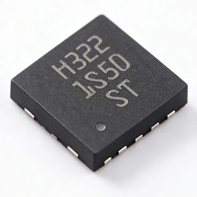
ST1S50PUR - 3A, 18V Synchronous Step-Down Converter | STMicroelectronics
The ST1S50PUR is a high-efficiency, synchronous step-down DC-DC converter from STMicroelectronics, designed to deliver up to 3A of continuous output current from an input voltage range of 4V to 18V. Housed in a compact DFN8 (3x3 mm) package, this device integrates both high-side and low-side power MOSFETs, eliminating the need for an external Schottky diode and simplifying PCB layout. The output voltage is adjustable from 0.8V to VIN, allowing flexibility for a wide range of applications. A synchronous buck converter is a type of DC-DC step-down regulator that uses two active switches (typically MOSFETs) instead of a diode for the low-side element, which significantly improves efficiency, especially at lower output voltages. This architecture is fundamental in power management ICs, where efficiency directly impacts battery life, thermal management, and system reliability. The ST1S50PUR belongs to the family of synchronous step-down converters, which are essential building blocks in modern electronic systems, from portable devices to industrial equipment. Key features of the ST1S50PUR include a fixed 1.5 MHz switching frequency, which allows the use of small, low-cost inductors and capacitors, reducing the overall solution footprint. The device offers a typical efficiency of 90% at 3A load, with a low quiescent current of 1.2 mA in light-load operation. It also features internal soft-start to limit inrush current, overcurrent protection, and thermal shutdown for robust operation. The DFN8 package has an exposed pad for enhanced thermal performance, with a thermal resistance of 40°C/W. The ST1S50PUR utilizes a current-mode control architecture, providing fast transient response and stable operation over a wide range of input and output voltages. The integrated MOSFETs have low RDS(on) (typically 120 mΩ high-side and 80 mΩ low-side), minimizing conduction losses. The device operates over a junction temperature range of -40°C to +150°C, making it suitable for demanding environments. Typical applications include point-of-load (POL) converters for FPGAs, DSPs, and microcontrollers, as well as power supplies for set-top boxes, networking equipment, and industrial control systems. The wide input voltage range also supports 12V and 24V bus systems, making it versatile for various power architectures. When designing with the ST1S50PUR, ensure proper input and output capacitor selection to maintain stability and minimize ripple. The exposed pad should be soldered to a large copper area for effective heat dissipation. The EN pin allows for power sequencing, and the soft-start feature prevents output overshoot during startup.

STNRG011ATR - Digital Power Controller for SMPS | STMicroelectronics
The STNRG011ATR is a digital power controller from STMicroelectronics designed for switched-mode power supplies (SMPS). It integrates a digital control core with a high-voltage startup cell, making it suitable for flyback, buck, and boost converter topologies. The device operates from an input voltage range of 8.5V to 23V and provides a gate drive output capable of sourcing 0.5A and sinking 0.8A. It is housed in a 16-pin SO-16 package, offering a compact solution for power supply designs. A digital power controller is a type of power management IC that uses digital signal processing to regulate output voltage and current, replacing traditional analog control loops. It sits within the hierarchy of power management ICs, which include linear regulators, switching regulators, and digital power controllers. Digital controllers offer advantages such as programmability, higher efficiency, and better transient response compared to analog counterparts. Key features of the STNRG011ATR include a programmable switching frequency up to 1 MHz, an integrated high-voltage startup cell that reduces standby power consumption, and a digital control loop that can be configured via an I2C interface. The device also includes protection features such as overcurrent protection, overvoltage protection, and thermal shutdown, ensuring reliable operation in demanding environments. The STNRG011ATR utilizes a digital control architecture with a dedicated state machine and a configurable PID compensator. This allows designers to optimize the control loop for specific power stage characteristics without changing external components. The integrated high-voltage startup cell enables fast startup and low standby power, making it ideal for applications requiring energy efficiency standards compliance. Typical applications include AC-DC adapters, USB Power Delivery (USB-PD) chargers, and industrial power supplies. The device's digital control capability allows for precise voltage and current regulation, which is essential for USB-PD applications that require multiple output voltage levels. Its wide input voltage range and high switching frequency support compact transformer designs, reducing overall solution size. When designing with the STNRG011ATR, ensure proper layout of the high-voltage startup cell and gate drive traces to minimize parasitic inductance. The I2C interface should be isolated from high-voltage areas to prevent noise coupling. Additionally, the thermal pad should be connected to a large copper area for effective heat dissipation.

STPM066S - 66V Step-Down DC-DC Converter | STMicroelectronics
The STPM066S is a high-voltage step-down DC-DC converter from STMicroelectronics, designed to deliver efficient power conversion in industrial and automotive applications. It operates from a wide input voltage range of 4.5V to 66V, making it suitable for 12V, 24V, and 48V bus systems. The device provides a continuous output current of up to 3A, with an adjustable output voltage down to 0.8V. Housed in a compact QFN-16 package (4x4 mm), the STPM066S integrates high-side and low-side MOSFETs, reducing external component count and simplifying PCB layout. A step-down DC-DC converter, also known as a buck converter, is a type of switching regulator that efficiently reduces a higher input voltage to a lower output voltage. Unlike linear regulators, which dissipate excess power as heat, buck converters use inductive energy storage and high-frequency switching to achieve efficiencies often exceeding 90%. This makes them essential in power management systems where thermal budget and battery life are critical. The STPM066S belongs to the broader category of power management ICs, specifically within DC-DC converters, and is a key building block in distributed power architectures. Key features of the STPM066S include a peak efficiency of 95%, a switching frequency adjustable from 200kHz to 2.2MHz, and a low quiescent current of 40uA in light-load mode. The device also offers a precision enable pin with hysteresis, soft-start to limit inrush current, and comprehensive protection features including overcurrent, overvoltage, and thermal shutdown. The integrated MOSFETs have low RDS(on) of 80mOhm (high-side) and 40mOhm (low-side), minimizing conduction losses. Technically, the STPM066S employs a current-mode control architecture, providing fast transient response and stable operation with a wide range of output capacitors. The adjustable switching frequency allows designers to optimize efficiency versus component size, while the external compensation pin offers flexibility in loop tuning. The device is available in a QFN-16 package with an exposed thermal pad, achieving a thermal resistance of 25°C/W, enabling reliable operation at high ambient temperatures. Typical applications include industrial power supplies, automotive infotainment systems, battery-powered equipment, and distributed power architectures in telecom and networking equipment. The wide input range and high efficiency make it ideal for pre-regulation in multi-rail systems, where it steps down a high-voltage bus to an intermediate rail for downstream LDOs or point-of-load converters. When designing with the STPM066S, ensure proper input and output capacitor selection to minimize voltage ripple and maintain stability. The bootstrap capacitor for the high-side driver must be placed close to the BST pin, and the feedback network should be routed away from the inductor to avoid noise coupling. Adequate copper pour on the thermal pad is essential for heat dissipation at high output currents.

STR-W6072S - 72W Off-Line PWM Controller w/ MOSFET | Sanken
The Sanken STR-W6072S is an off-line switching power supply controller IC with an integrated power MOSFET, housed in a TO-220F-5 (formed-leads) package. It operates in a fixed-frequency current-mode PWM topology between 60 kHz and 74 kHz, targets flyback converter designs up to approximately 72 W output, and combines the power switch and control circuitry on a single die to reduce BOM count in cost-sensitive adapters and auxiliary supplies. A switching power supply controller (also called an AC-DC converter IC or PWM controller IC) is a semiconductor that regulates output voltage in a switch-mode power supply (SMPS) by modulating the duty cycle of an internal or external power switch at high frequency. The STR-W6072S belongs to the AC-DC converter sub-category of power management ICs (PMICs), sitting inside a flyback converter topology that is the dominant architecture for sub-100 W isolated supplies such as appliance adapters, set-top box wall warts, and standby rails for white goods. Within the device, a current-mode PWM controller IC is co-packaged with a power MOSFET, eliminating the drive loop between separate controller and MOSFET components. Key features include integrated avalanche-rated 650 V MOSFET, automatic standby/burst-mode operation for sub-100 mW standby power, built-in soft-start, over-current protection (OCP) with auto-restart, over-voltage protection (OVP), thermal shutdown, and an under-voltage lockout (UVLO) on the VCC pin. The auxiliary winding feedback topology sets output voltage indirectly via the VCC supply, removing the need for an opto-isolator and TL431 in low-cost designs. The internal architecture uses a current-mode PWM control loop with leading-edge blanking, slope compensation, and a built-in oscillator. The Sanken STR-W6000S series is positioned as a cost-performance optimized family for digital TV, monitor, and appliance standby power, where the controller integrates the high-voltage startup circuit and eliminates external bias components. Compared to a discrete UC3842 + MOSFET implementation, the STR-W6072S achieves a much smaller PCB footprint and lower standby power, at the expense of peak output power ceiling. Typical applications include AC-DC adapters up to 72 W, auxiliary/standby supplies for white goods and industrial equipment, digital TV and monitor main power supplies, set-top box power bricks, and low-cost isolated DC-DC converters. Designers typically use it in quasi-resonant or hard-switched flyback configurations with a simple single-winding auxiliary feedback. When designing with the STR-W6072S, ensure the VCC auxiliary winding is wound to deliver 15 V to 20 V at nominal load so that VCC stays within the 8.5 V to 18 V operating range. Verify that peak drain current does not exceed the integrated MOSFET rating, and add a Y-capacitor and adequate common-mode choke on the input for EMI suppression to meet EN55022 Class B. This page synthesizes Sanken's official datasheet, current distributor pricing, verified drop-in alternatives in the same TO-220F footprint, and practical flyback design notes that are not collected in the equivalent value of a single product listing.
STR-W6072S - Off-Line PWM Controller with 800V MOSFET | Sanken
The Sanken STR-W6072S is an off-line PWM controller with an integrated 800V power MOSFET in a TO-220-5 (TO-220F-6 formed leads) package, designed for AC/DC flyback converters in the 60 kHz to 74 kHz switching range. It combines a current-mode PWM controller IC and a high-voltage avalanche-rugged MOSFET on one die, enabling compact, low-component-count SMPS designs. The STR-W6000S series targets cost-sensitive auxiliary and standby power supplies where a few external parts and built-in protection are required. An off-line PWM controller with integrated MOSFET (sometimes called a Power IC or Power Supply Control IC) is a category of power-management semiconductor that replaces a discrete PWM controller plus external MOSFET pair. Within the system hierarchy, this device sits between an analog PWM controller IC and a high-voltage switching MOSFET, integrating both functions to reduce BOM count and simplify EMI layout. The integrated approach also shortens high-current loops between the MOSFET drain, the transformer primary, and the controller's current-sense input, lowering radiated EMI. The STR-W6072S operates from a universal AC input (via a rectified 100 V to 400 V DC bus) and incorporates an auto-standby function that switches between normal PWM operation and burst oscillation under light-load conditions. This auto-standby behavior yields low standby power consumption, helping designs meet modern energy-efficiency regulations for home appliances and consumer electronics. Built-in protections include over-current protection (OCP), over-voltage protection (OVP), and thermal shutdown. Internally the device uses a current-mode control topology with slope-compensated peak current sensing through the MOSFET source. The integrated MOSFET's avalanche rating is published for unclamped inductive switching events, simplifying snubber design. Operating frequency is trimmed across the 60 kHz to 74 kHz band, allowing the designer to optimize transformer size versus switching loss. According to the manufacturer datasheet, fault protection covers over-temperature and over-voltage events, with thermal shutdown typically engaging above 150 °C junction. Typical applications for the STR-W6072S include low-to-medium-power AC/DC adapters, auxiliary and standby supplies in white goods, set-top box power supplies, and small appliance SMPS modules up to roughly 50 W output. Its 800 V drain rating provides wide margin on 265 V AC rectified inputs where reflected voltage spikes can stress the primary switch. When designing with the STR-W6072S, thermal management of the TO-220-5 tab is critical: the exposed metal tab is the primary heat path and must be soldered (or clipped) to a copper area on the PCB or to a small heatsink. Drain-voltage ringing under 265 V AC operation also demands an RCD snubber sized to the leakage inductance of the flyback transformer.

TC7660SCOA - 20mA Super Charge Pump Inverter | Microchip 8-SOIC
The Microchip TC7660SCOA is a 20 mA super charge pump DC-to-DC voltage converter in an 8-pin SOIC package that inverts +1.5V to +12V input to a corresponding -1.5V to -12V output using only two low-cost capacitors. The 'S' variant upgrades the industry-standard TC7660 with extended supply range, higher efficiency (98% typ), and lower quiescent current of 80 µA typ at VIN = 5V, eliminating inductors and the associated cost, board area, and EMI. A charge pump (also called a switched-capacitor voltage inverter) is a type of DC-DC converter that uses capacitors rather than inductors to store and transfer energy. Charge pumps belong to the switched-capacitor converter family within the broader power management IC hierarchy. Unlike inductive buck/boost converters, charge pumps are EMI-quiet and use only two external capacitors, making them ideal for low-current negative rail generation where simplicity and noise performance outweigh efficiency. Key features include 99.9% voltage conversion efficiency (typ), 20 mA output current capability, wide input voltage range up to +12V (vs 10V for original TC7660), and on-board oscillator at nominal 10 kHz frequency. The TC7660SCOA also supports a BOOST pin for higher switching frequencies when needed. The 8-SOIC package operates over -40°C to +85°C industrial temperature range with surface-mount assembly. The architecture uses a CMOS switched-capacitor voltage inverter with integrated MOSFET switches clocked by an internal RC oscillator. The doubler/inverter topology transfers charge from input to reservoir capacitor on one clock phase and inverts on the other, producing a negative output without inductors or transformers. The result is a compact, low-noise negative supply solution with predictable EMI signature. Typical applications include op-amp negative supply rails, LCD bias generators, data acquisition systems, EIA-232/EIA-422 level translators, and portable instrument negative rails. The 20 mA output comfortably drives a single op-amp negative rail or a small RS-232 transceiver charge pump supplement. When designing with this device, ensure external reservoir and pump capacitors are low-ESR types rated for the switching frequency, and observe the LV pin voltage derating requirements above +10V input to maintain reliability. This page synthesizes distributor pricing, drop-in alternatives, and practical design notes not found in the manufacturer datasheet.
TC7660SEOA - 20mA Super Charge Pump DC-DC Converter | Microchip
The Microchip Technology TC7660SEOA is a super charge pump DC-to-DC voltage converter that delivers up to 20 mA of negative output current from a +1.5 V to +12 V input, housed in an 8-pin SOIC (0.154", 3.90 mm width) package. It functions as an inverted switched-capacitor regulator that produces -Vin or 2Vin selectable output with only two external capacitors, eliminating inductors and their associated cost, size, and EMI. A charge pump DC-DC converter is a type of switching voltage regulator that uses capacitors rather than magnetic inductors to store and transfer energy. Charge pumps sit within the broader hierarchy of DC-DC converters -> switching regulators -> power management ICs -> semiconductors. They are favored in low-power, noise-sensitive designs because they generate no magnetic EMI and require only two capacitors, making them ideal for compact analog front ends where a small negative supply rail is needed without the bulk of an inverting buck-boost converter. Key features of the TC7660SEOA include pin-compatibility with the industry-standard 7660 footprint, a wide 1.5 V to 12 V input range that can be doubled to 12 V to 24 V using the internal oscillator doubling mode, and a typical quiescent current in the microamp range. The on-board CMOS oscillator nominally operates at 10 kHz, with an optional external clock input for synchronization. The device includes a BOOST pin reference, low output impedance (~55 ohm typical), and operates across the -40C to +85C commercial temperature range, suiting RS-232 drivers, op-amp negative rails, and portable instrumentation. Internally, the TC7660SEOA uses CMOS transistors configured as an H-bridge switched-capacitor network clocked by the on-chip oscillator. During one clock phase, the flying capacitor is charged to +Vin; during the alternate phase, it is flipped and discharged into the reservoir capacitor at -Vin. The architecture avoids the switching spikes common to inductive converters, and its symmetrical pinout supports cascading two devices for voltage doubling. Typical applications include generating the -5 V to -12 V rail for RS-232 transceivers, negative bias supplies for op-amps and LCD contrast, low-current analog signal conditioning, and portable data-acquisition systems. When designing with this device, keep the flying capacitor ESR low (typically 10 uF) and place reservoir capacitors close to pins 5 and 8 to minimize ripple and load-transient overshoot. This page synthesizes distributor pricing, drop-in alternatives, and practical design notes that go beyond the manufacturer datasheet to help engineers select and source the TC7660SEOA with confidence.
TDA21490 - 90A OptiMOS Smart Power Stage, PQFN 5x6 | Infineon
The Infineon TDA21490 is a 90 A integrated smart power stage that co-packages a low-quiescent-current synchronous buck gate-driver IC with high-side and low-side OptiMOS MOSFETs in a thermally enhanced PQFN 5x6 (PG-IQFN-39-7) package. Input voltage (VIN) ranges from 4.25 V to 16 V, VCC and VDRV supply from 4.25 V to 5.5 V, maximum switching frequency 1500 kHz, and the device integrates 5 mV/A on-chip MOSFET current sensing with temperature-compensated reporting. The co-packaged architecture minimizes parasitics between driver and FETs for efficient low-voltage, high-current multiphase buck conversion. What is a smart power stage? A smart power stage is an integrated power-conversion building block that combines a PWM gate driver with the high-side and low-side MOSFETs of a synchronous buck converter into a single package. It belongs to the DrMOS (Driver plus MOSFET) family, which itself falls under multiphase buck regulators, which in turn are a subclass of DC-DC converters and the broader power management IC category. Smart power stages are the modern way to deliver the high currents (tens of amps to >100 A per phase) demanded by xPUs, ASICs, and SoCs while keeping PCB real estate small and switching-node ringing low. Key features include 5 mV/A accurate current-sense output, integrated bootstrap switch, OCP/OVP/UVP fault protection, a 3.3 V tri-state PWM input with wide compatibility, and a thermally optimized exposed-lead package. The OptiMOS technology enables best-in-class efficiency at low duty cycles that are required for sub-1 V core rails. The current reporting is temperature compensated, removing a calibration step typically needed by external inductor DCR sense networks. According to the Infineon datasheet, the package's lead-frame design enables direct heatsinking to the PCB copper pour for sustained 90 A operation without external heatsinks in many applications. Architecturally, the TDA21490 integrates the bootstrap diode, smart self-bootstrap refresh, adaptive dead-time control, and thermal flag output. Compared with a discrete DrMOS implementation (separate driver + two MOSFETs + Schottky + sense resistor), the TDA21490 reduces the BOM count by roughly 5 to 7 parts per phase and shrinks the converter footprint by an estimated 30 to 50 percent, while the matched driver-to-FET timing reduces dead-time loss and shoot-through risk. The internal current mirror eliminates the external current-shunt amplifier typical of controller-based designs. Typical applications include AI server VRMs, GPU and graphics card core power, HPC and ASIC multiphase buck regulators, telecom/datacenter 48 V-to-POL converters, and high-current DDR5 memory power. The PQFN 5x6 footprint is shared across the OptiMOS power-stage family, enabling designers to scale load current by adding phases without re-laying out the board. Designers should carefully follow Infineon's layout guidelines to minimize switch-node ringing, place input ceramic capacitors directly at the VIN pins, and use the thermal flag to throttle or shut down phases during faults. This page synthesizes distributor pricing, drop-in alternatives, and practical design notes that complement the manufacturer datasheet.
TDA21590AUMA1 - 90A Smart Power Stage | Infineon
The Infineon TDA21590AUMA1 is a 90 A integrated smart power stage with a 4.25 V to 16 V input range and switching frequency up to 1500 kHz, packaged in a 5 mm by 6 mm PQFN. It combines a low-quiescent-current synchronous buck gate-driver IC, control circuitry, synchronous MOSFETs, and an active-diode structure in one package. The active diode provides low forward voltage behavior similar to a Schottky diode with very little reverse-recovery charge. This integration supports compact, efficient converter designs for CPUs, GPUs, DDR memory arrays, telecom equipment, and other high-current power-conversion systems. A smart power stage is an integrated power-conversion component that combines control and switching functions into a module. In system terms, it belongs to the DC-DC converter and voltage-regulator hierarchy, then to the broader power-management semiconductor category. Its purpose is to reduce external switching components, simplify PCB layout, improve thermal transfer, and provide controlled MOSFET and driver timing within a compact package. The TDA21590 is therefore positioned for demanding point-of-load and multiphase converter applications rather than ordinary low-power linear regulation. The manufacturer identifies optimized package construction for PCB layout, heat transfer, driver and MOSFET control timing, and minimal switch-node parasitic inductance. The integrated synchronous MOSFET arrangement can improve conversion efficiency compared with a discrete low-side rectifier implementation. The active-diode structure is intended to reduce reverse-recovery charge, which can reduce switching stress in applications where current paths alternate or transient current is significant. Its 90 A output rating is a headline capability, but actual regulator performance depends on controller configuration, switching frequency, inductor selection, thermal design, and current limits. TDA21590 devices are intended for high-frequency, low-profile DC-DC converters used by CPUs, GPUs, and DDR memory arrays, as well as telecom power systems. Controlled and uncontrolled operating configurations are referenced in the product documentation. For a processor or accelerator rail, the stage can be paired with a multiphase controller and suitable power inductors. For memory or telecom conversion, its compact package can help reduce board area while retaining high current capability. The device should be selected only after checking the complete application circuit against the manufacturer datasheet, including absolute maximum ratings, electrical characteristics, exposed-pad connections, pin definitions, and thermal conditions. Design attention should center on switch-node layout, input and output capacitor placement, exposed-pad thermal management, and controller dead-time behavior. The package is optimized for heat transfer, but thermal performance still depends on copper area, thermal vias, board stack-up, ambient temperature, and the power dissipated by the integrated stage. Inductors must be selected for the required current rating and saturation margin, while capacitors must be placed close to the power-stage pins to limit high-current loop area. Because the provided data does not include a complete electrical parameter table or a verified pin-by-pin package drawing, those details remain marked for engineering review. This product page combines the verified manufacturer description, distributor listings, pricing evidence, package information, and cross-reference results for TDA21590AUMA1. It distinguishes verified facts from parameters requiring datasheet confirmation and avoids presenting unrelated motor-driver listings as valid replacements. The most important procurement checks are the 90 A rating, 4.25 V to 16 V input range, 1500 kHz maximum switching frequency, and exact 5 mm by 6 mm PQFN footprint.
TDA22590 - 90A Integrated Power Stage | Infineon
The Infineon TDA22590 is a 90 A industrialOptiMOS 6 integrated power stage for high-current, low-voltage synchronous buck conversion, with a 4.25 V to 16 V input range, 0.225 V to 5.5 V output range, and a 4 mm × 6 mm UFLGA package. It combines a gate-driver IC, control MOSFET Q1, synchronous MOSFET Q2, and a Schottky diode in one power-stage package. On-chip MOSFET current sensing and reporting at 5 μA/A provides a proportional measurement signal for control and telemetry. VCC and VDRV operate from 4.5 V to 5.5 V. An integrated smart power stage is a DC-DC converter subsystem that combines semiconductor switching elements and their drive circuitry in one package. In the power hierarchy, it belongs to synchronous buck converters, which are DC-DC converters and power-management devices. Compared with a discrete synchronous-buck implementation, the integrated arrangement can reduce external switching-component count and simplify high-current layout, while still requiring careful inductor, capacitor, thermal, and gate-drive design. The TDA22590 provides up to 90 A output and supports conversion from 4.25 V to 16 V down to 0.225 V to 5.5 V. That range suits CPU, GPU, FPGA, DDR memory, telecom, controlled, and uncontrolled power-conversion systems identified in the manufacturer materials. Its integrated MOSFETs support a compact synchronous-buck topology, while the current-reporting feature can assist a controller in monitoring phase current. The device is designed for demanding multiphase rails where low profile, high current, and integrated power semiconductors are important. The 4 mm × 6 mm package supports placement close to the load, but package current capability is not the same as continuous application current: output current depends on switching frequency, inductor selection, PCB copper area, thermal conditions, duty cycle, and control-loop settings. Typical uses include server processor rails, accelerator supplies, memory-array regulators, FPGA power systems, and telecom power converters. In these systems, the TDA22590 can be arranged with external inductors, input capacitors, output capacitors, and a controller implementing multiphase power delivery. The low quiescent-current synchronous-buck gate-driver architecture helps reduce standby demand while the integrated MOSFETs handle the power path. A critical design consideration is the separation of power and signal paths. VIN, VCC, VDRV, PG, current-reporting, ground, and switch-node connections must follow the manufacturer layout guidance, with very low-inductance power loops and careful placement of high-current copper. The UFLGA package is not represented by an exact pinout in the supplied verified data, so the complete pin map cannot be safely reconstructed here. The manufacturer datasheet should remain the authority for pin numbering, exposed-pad treatment, capacitance values, and recommended layout. This page combines verified manufacturer specifications, source links, pricing fields, application guidance, and validation notes for engineers evaluating the TDA22590 in high-current power-conversion designs.
TDA235E5 - 2A/mm² Dual-Phase Smart Power Stage | Infineon
The Infineon TDA235E5 is a dual-phase smart power stage integrating OptiMOS 6 MOSFETs with a dual-phase driver IC, delivering over 2 A/mm² power density and up to 300 A peak current in a compact 6 x 6 x 0.8 mm³ package. Announced September 2026, it targets next-generation AI accelerators and vertical power delivery modules where power density is the limiting factor for compute scaling. The device combines monolithic gate driver and power stage integration, eliminating parasitic inductance between driver and FET that limits conventional discrete designs. A smart power stage is a fully integrated point-of-load (POL) building block that contains the high-side and low-side MOSFETs, the gate driver, current sensing, and protection in one package. Smart power stages sit inside the broader power management hierarchy: voltage regulator module (VRM) -> multiphase buck controller -> smart power stage -> POL conversion for CPUs, GPUs, and AI ASICs. By integrating driver and FETs, the smart power stage minimizes dead time, switching losses, and parasitic loop inductance, enabling higher switching frequency and tighter regulation. Key features include 2 A/mm² power density, 300 A peak current per stage, dual-phase architecture for multiphase VR topologies, integrated current-temperature telemetry for control ICs, and liquid cooling support. The 6 x 6 x 0.8 mm³ package enables placement directly under the AI accelerator cold plate, supporting vertical power delivery (VPD) architectures that reduce PCB current path length by an order of magnitude compared to lateral delivery. Typical applications include AI accelerator core rails (HBM, GPU, ASIC), hyperscale data center vertical power delivery, 48 V to point-of-load conversion stages, server CPU/GPU multiphase VRs, and high-performance computing (HPC) POLs. The TDA235E5 also supports liquid-cooled cold-plate designs common in next-generation AI server racks. When designing with TDA235E5, ensure the multiphase PWM controller is Infineon-compatible (OptiMOS family), follow the PCB layout guideline for thermal pad connection to inner copper layers, and verify current sharing accuracy between the two integrated phases. The integrated current telemetry outputs must be routed to the controller's IMON input with minimal noise pickup. This page synthesizes Infineon press release specifications, distributor stock information, and practical VR design notes not collated in the original press brief.
TDA38807XUMA1 - 6A Sync Buck Regulator, 2.7-16V Input | Infineon
The Infineon TDA38807XUMA1 is a 6 A synchronous buck (step-down) DC-DC voltage regulator housed in a 14-pin UFQFN exposed-pad package. It accepts a wide 4 V to 16 V input (2.7 V to 16 V with external 3.3 V VCC bias) and produces an adjustable output from 0.9 V to 5.5 V with ±0.5% reference accuracy, targeting industrial point-of-load (POL) and distributed power architectures. The device uses internal MOSFET switches and requires no external Schottky diode or compensation network, simplifying PCB layout and reducing BOM cost. A buck (step-down) DC-DC switching regulator is a power management integrated circuit that converts a higher DC input voltage to a lower, regulated DC output voltage by rapidly switching an internal power FET and storing energy in an external inductor. The buck regulator sits within the broader taxonomy of voltage regulators, which also includes linear regulators (LDO), boost converters, and buck-boost converters - all of which belong to the power management IC family that conditions supply rails for downstream digital and analog loads such as processors, FPGAs, ASICs, and memory. Key features include a precision 0.9 V ±0.5% reference, stable operation with low-ESR ceramic output capacitors, internal soft-start, cycle-by-cycle current limiting, thermal shutdown, and a power-good indicator. According to the Infineon datasheet, the regulator operates at typical switching frequencies compatible with 2 MHz-class conversion and supports 100% duty-cycle operation for low-dropout scenarios. The TDA38807 employs a voltage-mode control architecture with internal loop compensation, eliminating the need for external RC components. Its 14-pin UFQFN package exposes the thermal pad on the bottom side, allowing the high-side and low-side FET dissipation to be conducted directly into the PCB copper. The internal MOSFETs are specified for continuous 6 A output current across the full industrial temperature range of -40 °C to +125 °C junction temperature. Typical applications include FPGA core and I/O rail generation, ASIC POL supplies, networking switch ASICs, industrial 12 V bus regulation, and telecom board-level power. In all of these, the wide input range and high efficiency of the synchronous topology replace less efficient linear regulators and shrink the power dissipation budget. When designing with the TDA38807, place input ceramic capacitors (typically 22 µF X7R) within 5 mm of the VIN and PGND pins to minimize switching-node ringing. The exposed pad must be soldered to a continuous ground copper pour of at least 25 mm² to keep junction temperature within safe limits at 6 A continuous load. This page synthesizes distributor pricing, same-package drop-in alternatives, and application-specific design notes not found in the manufacturer datasheet.
TDA38813XUMA1 - 12A Sync Buck Regulator, 2.7-16V | Infineon
The Infineon TDA38813XUMA1 is a 12 A fully integrated synchronous DC-DC buck regulator using fast Constant On-Time (COT) control, housed in a 21-lead PowerUFQFN package. It accepts a wide input voltage range of 2.7 V to 16 V (with external VCC bias), provides an adjustable output from 0.9 V, and delivers up to 12 A continuous load current with internal MOSFETs. A buck regulator (also called a step-down switching converter) is a power management integrated circuit that converts a higher DC input voltage to a lower DC output voltage with high efficiency by rapidly switching an internal MOSFET between ON and OFF states and filtering the resulting pulsed waveform through an LC network. Buck regulators sit within the hierarchy: synchronous buck regulator -> DC-DC switching converter -> voltage regulator -> power management IC -> semiconductor. They are preferred over linear regulators (LDOs) for high-current applications because switching conversion avoids the VIN-VOUT current-passing losses that would make a 12 A LDO impractical. Key features of the TDA38813XUMA1 include: 0.5% reference voltage accuracy, stable operation with ceramic output capacitors (no external compensation required), and an internal 16 V bias capable of supporting wide VIN operation. The COT control scheme simplifies design by eliminating the loop-compensation network and provides fast transient response while maintaining tight line and load regulation. It supports external VCC bias (3.3 V) for higher efficiency at high VIN. Architecturally, the device integrates high-side and low-side MOSFETs, the gate driver, the COT controller, and a precision reference in a single PowerUFQFN package with an exposed thermal pad. The COT modulator samples VOUT directly and modulates the high-side on-time as a function of VIN, giving a near-fixed switching frequency in continuous conduction mode. Typical applications include 12 V rail point-of-load (POL) conversion in servers and storage systems, distributed DC-DC in networking switches, FPGA and ASIC core/IO rails, and industrial automation boards. Design considerations include input/output capacitor selection (low-ESR ceramic recommended), bootstrap capacitor sizing for the high-side gate drive, and thermal pad soldering for heat extraction under heavy load.