DC-DC Converters
بەرهەمەکان (770+)

TPS560430XDBVR - 36V, 0.6A Synchronous Buck Converter | Texas Instruments
The Texas Instruments TPS560430XDBVR is a 4V to 36V input, 0.6A continuous output synchronous step-down SIMPLE SWITCHER® power converter housed in a 6-pin SOT-23 (DBV) package. This wide-Vin converter integrates both high-side and low-side MOSFETs in a compact footprint, supports an adjustable output from 1V to 34.2V, and operates at 1.1 MHz switching frequency to minimize external inductor and capacitor size. Its 4V to 36V input range makes it well-suited for industrial 24V rails and automotive load-dump-tolerant applications. A synchronous buck converter is a switching DC-DC topology that uses actively controlled high-side and low-side MOSFETs to step down a higher input voltage to a lower regulated output voltage. Buck converters belong to the broader class of voltage regulators within power management ICs (PMICs), and the synchronous variant replaces the conventional Schottky rectifier with a low-side MOSFET to improve efficiency, especially at light loads. SIMPLE SWITCHER is TI's family designation for easy-to-use, externally-compensated, wide-Vin synchronous buck ICs aimed at general-purpose point-of-load regulation. Key features of the TPS560430XDBVR include 0.6A continuous load capability, 1.1 MHz typical switching frequency (with a 2.1 MHz sibling option in the family), pulse frequency modulation (PFM) for light-load efficiency, an enable pin for power sequencing, internal soft-start, and thermal shutdown. The 6-pin SOT-23-6 footprint enables use in space-constrained designs while still allowing thermal dissipation for a 0.6A load on a properly sized copper pour. Technically, the TPS560430 uses peak current-mode control with internal compensation, a precision bandgap reference, and adaptive dead-time control between the high-side and low-side FETs to prevent shoot-through. The wide 4V-36V input range and 0.6A output deliver a flexible platform for 24V industrial buses, 12V automotive systems, and battery-powered applications where the input can vary widely during transients. Typical applications include industrial 24V sensor and actuator rails, automotive infotainment and body controllers, point-of-load regulation after a higher-voltage bus, and general-purpose 5V/3.3V rails in PLC and factory automation modules. The wide input margin accommodates both nominal and transient conditions without requiring pre-regulation. When designing with this part, ensure the input capacitor handles the 36V maximum and the inductor is rated for the 0.6A peak current. Use the WEBENCH® Power Designer tool to size L, Cin, Cout, and feedback resistors for the specific VIN/VOUT combination. This page synthesizes distributor pricing, drop-in alternatives, and practical design notes not found in the manufacturer datasheet.
TPS560430YDBVR - 36V, 600mA Synchronous Buck Converter | TI
The Texas Instruments TPS560430YDBVR is a 4V to 36V input, 600mA synchronous step-down SIMPLE SWITCHER® power converter housed in a 6-pin SOT-23 (DBV) package. The Y-suffix device variant specifies the 2.1 MHz switching-frequency option, which favors small external inductor and capacitor sizes and keeps the fundamental switching harmonic above the AM broadcast band for easier EMI filtering in sensor and instrumentation modules. Integrated high-side and low-side MOSFETs eliminate the external Schottky diode, reducing BOM count and total solution footprint. According to TI product page, the device delivers 600 mA continuous load current across an operating temperature range of -40 °C to +125 °C. What is a synchronous step-down DC-DC converter? A buck converter is a switched-mode power supply (SMPS) topology that steps a higher DC input down to a lower DC output. Synchronous buck converters replace the traditional rectifier diode with a low-side MOSFET, which significantly improves efficiency at light loads and reduces conduction losses. Within the broader power-management IC hierarchy, this part belongs to the SIMPLE SWITCHER® family - a category of point-of-load regulators designed for ease of use, low external component count, and predictable behavior in industrial and automotive distributed-power systems. Key features include an internal compensation network that removes external compensation components, an EN pin for power sequencing and shutdown, and PFM (Pulse Frequency Modulation) at light loads to extend efficiency in idle conditions. The 2.1 MHz switching frequency (Y variant) keeps the converter above the AM band, simplifying input-filter design. Quiescent current is rated at approximately 80 µA typical, and the converter supports output voltages down to 1 V. The SOT-23-6 package is the industry-standard micro-outline footprint for low-power synchronous bucks. The TPS560430YDBVR integrates control logic, gate drivers, and power FETs into one die, using peak current-mode control for stable loop response and predictable inductor selection. The architecture supports both forced PWM and PFM modes, allowing designers to trade light-load efficiency for predictable output ripple. The wide 4 V-36 V input range supports direct connection to industrial 24 V rails, automotive 12 V battery systems, and eMeters without an upstream pre-regulator. Typical applications include industrial automation sensors, factory equipment modules, portable instrumentation, and automotive accessory power rails. The 600 mA rating suits sub-system loads such as microcontrollers, transceivers, and display backlights. The wide VIN range and small package also make it attractive for distributed POL (point-of-load) power in space-constrained designs. When designing with this part, follow the datasheet's recommended inductor and capacitor values for the 2.1 MHz variant to maintain stability across the full duty-cycle range. Place the input bypass capacitor as close as possible to VIN and GND to minimize switching-node ringing and EMI. This page synthesizes verified distributor pricing, same-brand drop-in alternatives, and practical design notes not found on the manufacturer product page alone, giving you a single-page engineering reference for the TPS560430YDBVR.

TPS561201DDCR - 17V 1A Synchronous Buck | Texas Instruments
The TPS561201DDCR is a 1A synchronous step-down (buck) converter from Texas Instruments, operating from a 4.5V to 17V input. It provides an adjustable output from 0.76V to 7V, switching at a fixed 580kHz. Housed in a 6-pin SOT-23-THN (DDC) package measuring 1.6mm x 2.9mm, it is designed for space-constrained, cost-sensitive point-of-load applications. A synchronous step-down voltage regulator is a DC-DC converter that uses two actively controlled switches (high-side and low-side MOSFETs) to efficiently lower a higher DC voltage to a lower regulated voltage. Unlike asynchronous regulators, the low-side switch replaces the freewheeling Schottky diode, reducing conduction losses and improving efficiency. This converter belongs to the broader family of switch-mode power supplies (SMPS) within power management ICs. Key features include D-CAP2 control, which simplifies loop compensation by requiring only a low-ESR ceramic output capacitor for stable operation. The device has an enable pin for power sequencing, fixed soft start to limit inrush current, and pulse skip mode for light-load efficiency. The quiescent current is only 0.4mA typical, contributing to high light-load efficiency. The device integrates a synchronous rectifier, eliminating an external Schottky diode and reducing board area. Internal cycle-by-cycle current limit and thermal shutdown protect the IC. The fixed 580kHz switching frequency offers a balanced trade-off between efficiency and component size, enabling small inductors and output capacitors. D-CAP2 mode also provides fast transient response, making it suitable for processors and FPGAs with dynamic loads. Typical applications include set-top boxes, smart TVs, networking equipment, industrial control systems, white goods, and battery-powered devices. On a 12V industrial bus, it can produce clean 3.3V or 5V rails for MCUs and I/O. The enable pin supports power sequencing in multi-rail systems. When designing with this part, use approximately 10uF input and 22uF output capacitance placed close to the device. Because the SOT-23 package is small, pay careful attention to thermal dissipation; at higher power loss a larger copper area is necessary to keep the junction temperature within the -40C to +125C range.
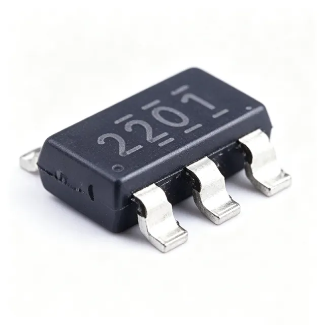
TPS562201DDCT - 2A 17V Sync Buck Converter | Texas Instruments
The Texas Instruments TPS562201DDCT is a 2A synchronous step-down (buck) converter in a compact 6-pin SOT-23-Thin (DDC) package, operating from a 4.5V to 17V input and producing an adjustable output from 0.768V to 7V at a fixed 580 kHz switching frequency. It integrates both high-side and low-side MOSFETs, eliminating the need for an external Schottky diode. A DC-DC switching regulator converts a higher input voltage to a lower regulated output using power switches and an inductor, offering far higher efficiency than a linear regulator. Within the power management IC hierarchy, the TPS562201 belongs to the synchronous buck converter family and is part of TI's D-CAP2 controller portfolio for point-of-load (POL) rails. Key features include the D-CAP2 control architecture, which provides fast transient response and supports both low-ESR and ceramic output capacitors with internal compensation, so no complex loop design is needed. Eco-mode pulse-skip operation maintains high efficiency at light loads by reducing switching frequency, while the 580 kHz fixed frequency allows small inductors and capacitors. Technically, the internally compensated adaptive on-time loop reacts within microseconds to load steps, making the part well suited to processor core and I/O rails. Internal soft-start limits inrush current, and the device is specified over a -40C to +125C junction temperature range in the 2.9 mm x 1.6 mm SOT-23-Thin package. Typical applications include 5V and 12V distributed-power point-of-load regulation, networking and telecom equipment, industrial automation systems, set-top boxes, and digital TV power supplies, where the 17V maximum input accepts 12V rails with headroom. Design consideration: keep the output voltage within the 0.768V to 7V range and use the datasheet-recommended ceramic output capacitance for D-CAP2 stability; place input decoupling capacitors as close as possible to the VIN and GND pins. This page synthesizes distributor pricing, drop-in alternatives, and practical design notes not found in the manufacturer datasheet.
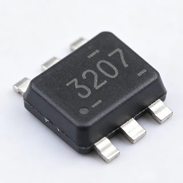
TPS563207DRLR - 3A 17V Synchronous Buck Converter | TI
The Texas Instruments TPS563207DRLR is a simple, easy-to-use 3-A synchronous buck converter in a compact 6-pin SOT-563 (DRL) package measuring just 1.6 mm x 1.6 mm. It accepts an input voltage range of 4.3 V to 17 V and produces an adjustable output down to 0.806 V, making it a space-saving point-of-load power solution. A DC-DC switching regulator (step-down converter) converts a higher input voltage to a lower regulated output using power MOSFET switches, an inductor, and output capacitors. Synchronous buck converters replace the freewheeling diode with a second MOSFET for higher efficiency. Within the power-management IC hierarchy, the TPS563207 is a monolithic buck regulator with integrated high-side and low-side FETs. Key features include D-CAP2 mode control for fast transient response and support of low-ESR output capacitors such as specialty polymer and ultra-low-ESR ceramic types. Fixed-frequency operation in Forced CCM (FCCM) mode maintains small output ripple even at light loads. The 3-A rating with integrated FETs minimizes external component count, and the tiny SOT-563 footprint suits dense PCB layouts. The device is specified from -40C to +125C junction temperature. Internally, D-CAP2 control combines a wide-bandwidth error amplifier with an adaptive on-time generator, enabling near-constant frequency operation and quick response to load steps with minimal output capacitance. Internal compensation and soft-start reduce design effort and board area. Typical applications include 5 V and 12 V rail point-of-load regulation for networking equipment, SSDs and storage, industrial PCs, FPGA/ASIC auxiliary rails, and consumer electronics. The 17-V maximum input covers 12-V buses with margin. Design tip: choose the inductor value and output capacitors per the TI datasheet equations; FCCM mode favors low ripple, while the 0.806-V feedback reference supports low-voltage cores. Verify thermal performance, as the small DRL package dissipates heat mainly through the PCB.

TPS566231 - 6A 18V Sync D-CAP3 Buck Regulator | TI
The Texas Instruments TPS566231 is a cost-effective, high-voltage-input synchronous step-down voltage regulator with integrated FETs, delivering up to 6A of continuous output current. It operates from a 3V to 18V input range, provides an adjustable output down to 0.6V, and comes in a 9-pin PowerVFQFN (RQF) package with pulse skip mode for high light-load efficiency. A synchronous buck converter is a type of DC-DC step-down regulator that uses two integrated transistors (high-side and low-side MOSFETs) to efficiently convert a higher input voltage to a lower output voltage. Unlike asynchronous converters that use a diode for the low-side, synchronous converters replace it with a low-resistance MOSFET, reducing conduction losses and improving efficiency, especially at high output currents. The TPS566231 belongs to the broader family of switching voltage regulators, essential power management ICs that convert and stabilize supply rails in electronic systems. Key features include ultra-low quiescent current (ULQ) for low-bias operation, adjustable soft-start via the SS pin, and up to 98% duty cycle support for low dropout between input and output. Protection is comprehensive: overvoltage protection (OVP), overcurrent protection (OCP), undervoltage lockout (UVLO), overtemperature protection (OTP), and undervoltage protection (UVP) with hiccup mode. The PG (power good) pin is available on the TPS566231P variant for power sequencing in multi-rail systems. The device uses TI's D-CAP3 control architecture, which provides fast transient response without external compensation, simplifying design. Integrated FETs and the compact 9-pin PowerVFQFN package minimize board space, while datasheet efficiency curves show peak efficiency above 90% for typical 12V-to-5V conversions. Typical applications include point-of-load (POL) converters in networking equipment, servers, storage systems, and industrial automation, powering FPGAs, ASICs, and processors where 6A capability and a wide 3V-to-18V input range matter. Pulse skip mode maintains high efficiency at light loads. When designing, select input and output capacitors carefully for stability and low ripple, and use the SS pin to control inrush current during startup.
TPS57140QDGQRQ1 - 42V 1.5A AEC-Q100 Buck Converter | TI
The Texas Instruments TPS57140QDGQRQ1 is an automotive-qualified 42 V, 1.5 A step-down (buck) switching regulator with an integrated 200 mOhm high-side MOSFET, housed in a 10-pin thermally enhanced HVSSOP/MSOP-PowerPAD (DGQ) package. It accepts 3.5 V to 42 V input and produces an adjustable output from 0.8 V to 39 V with peak efficiency at automotive input rails. A DC-DC buck converter is a switching voltage regulator that steps a higher DC voltage down to a lower one using an internal switch, an inductor, and a diode (or synchronous rectifier). Within the power-management hierarchy - voltage regulator -> switching regulator -> step-down converter -> point-of-load regulator - the buck converter is the workhorse of every automotive electronic control unit, converting battery or load-dump-derived rails into clean, efficient low voltages. Key features include AEC-Q100 qualification for 42 V input operation (covering 12 V and 24 V automotive battery systems plus load-dump transients), TI SWIFT (TM) architecture with peak current-mode control for simple external compensation, and Eco-Mode (TM) pulse-skip operation that reduces no-load regulated supply current to just 116 uA. Shutdown current drops to 1.5 uA when the enable pin is pulled low, extending battery life in always-on modules. Technical depth: the current-mode topology provides inherent cycle-by-cycle current limiting, fast transient response, and a single compensation network. The nonsynchronous design (external catch diode) gives freedom to optimize diode voltage rating and thermal placement. The integrated 200 mOhm high-side FET minimizes conduction loss, while the adjustable RT/CLK pin sets switching frequency and supports synchronization to an external clock for EMI-sensitive designs. Typical applications include automotive infotainment and cluster power supplies, camera modules and ADAS sensor rails, body electronics and lighting pre-regulators, and industrial 24 V bus point-of-load conversion. The wide 42 V input rating makes it equally suited to 12 V and 24 V systems without front-end pre-regulation. Design consideration: the nonsynchronous output requires a properly rated Schottky catch diode; at high VIN-to-VOUT ratios, diode loss dominates, so select a 40-60 V Schottky with low reverse leakage at operating temperature. Keep the PowerPAD soldered to a generous ground pour for thermal relief. This page synthesizes distributor pricing, drop-in family alternatives, AEO-optimized FAQs, and practical design notes not found in the manufacturer datasheet, based on data verified 2026-09-10.

TPS57160QDGQRQ1 - 60V 1.5A Buck Converter AEC-Q100 | TI
The Texas Instruments TPS57160QDGQRQ1 is a 1.5 A, 60 V automotive-grade step-down (buck) DC-DC switching regulator with an integrated 200-mohm high-side MOSFET, Eco-Mode control, and an adjustable output from 0.8 V to 58 V, housed in a 10-pin thermally enhanced MSOP-PowerPAD (DGQ) package. A buck converter, or step-down regulator, is a switching power-conversion IC that efficiently reduces a higher input voltage to a lower regulated output by switching an internal or external transistor at high frequency and filtering the result with an inductor and capacitors. Within the power management hierarchy, it sits under DC-DC converters, a subset of voltage regulators, and complements LDOs where conversion efficiency matters more than ultra-low noise. Key features include a wide 3.5 V to 60 V input range with AEC-Q100 automotive qualification, current-mode control that simplifies external compensation, and TI Eco-Mode pulse-skip operation that cuts no-load input supply current to 116 uA. Shutdown supply current via the enable pin is only 1.5 uA, critical for always-connected automotive modules that must minimize quiescent battery drain. Architecturally, the integrated low-drain-to-source on-resistance high-side MOSFET and its gate-drive circuitry inside the package allow high efficiency while keeping junction temperature low at high output currents. Internally fixed undervoltage lockout is set at 2.5 V and is adjustable via the enable pin for tighter input supervision. A RT/CLK pin supports resistor-programmed switching frequency as well as synchronization to an external clock, easing EMI planning in multi-converter systems. Typical applications include automotive 12 V and 48 V battery-rail point-of-load supplies, industrial 24 V bus step-down power, and telecom or avionics wide-input auxiliary rails feeding microcontrollers, CAN transceivers, and sensors. The 60 V rating provides ample surge headroom on load-dump-prone automotive inputs. When designing with this part, keep the PowerPAD soldered to a substantial copper ground plane for thermal performance, and verify compensation network values against the switching frequency chosen. Non-synchronous topology means a proper external catch diode must be selected for peak currents. This page synthesizes distributor pricing, drop-in alternatives, comparison tables, and practical design notes not found in the manufacturer datasheet alone.

TPS60400-Q1 - 60mA Charge Pump Inverter | TI Automotive
The TPS60400-Q1 is an unregulated charge pump voltage inverter from Texas Instruments, designed to generate a negative output voltage from a positive input supply ranging from 1.8 V to 5.25 V. It delivers up to 60 mA of output current and requires only three small 1-µF ceramic capacitors for operation. The device is AEC-Q100 qualified for automotive applications, ensuring reliability in harsh environments. The TPS60400-Q1 features a variable switching frequency that reduces operating current in applications with a wide load range and enables the use of low-value capacitors, making it an efficient and compact solution for generating negative supply rails. A charge pump voltage inverter is a type of DC-DC converter that uses switched capacitors to invert the polarity of an input voltage. Unlike inductive-based converters, charge pumps do not require inductors, which reduces electromagnetic interference (EMI) and simplifies PCB layout. The TPS60400-Q1 belongs to the TPS6040x-Q1 family of charge pump inverters, which are part of the broader category of switching regulators and power management ICs. These devices are essential in systems where a negative supply is needed for analog circuits, such as operational amplifiers, comparators, and data converters. Key features of the TPS60400-Q1 include its wide input voltage range of 1.8 V to 5.25 V, 60 mA output current capability, and low quiescent current due to variable frequency operation. The device operates with a switching frequency that adjusts based on load, optimizing efficiency across the load range. It also features a shutdown mode to reduce power consumption when the output is not needed. The TPS60400-Q1 is available in the small SOT-23 (DBV) package, which is ideal for space-constrained automotive and portable applications. Technically, the TPS60400-Q1 uses a charge pump architecture with an internal oscillator and switching transistors. The variable frequency control reduces switching losses at light loads, improving efficiency. The device can also be configured to generate a doubled positive output (2Vin) or a divided output (Vin/2) by connecting the capacitors differently, providing flexibility in system design. The output is unregulated, so the output voltage tracks the input voltage minus a small drop, which is acceptable for many analog applications. Typical applications include generating a negative rail for operational amplifiers in automotive sensor interfaces, powering LCD bias circuits, and providing a negative supply for audio amplifiers and data converters. The TPS60400-Q1 is also used in battery-powered devices where a negative voltage is required for analog circuitry. Its small footprint and minimal external components make it an attractive choice for compact designs. When designing with the TPS60400-Q1, it is important to place the three 1-µF ceramic capacitors close to the device to minimize parasitic inductance and ensure stable operation. The input capacitor should be placed between the IN pin and ground, and the output capacitor between the OUT pin and ground. The flying capacitor connects between the C1+ and C1- pins. Proper layout is critical to achieve the specified output ripple and efficiency.

TPS60400DBVR - 60mA Charge Pump Inverter | Texas Instruments
The Texas Instruments TPS60400DBVR is an unregulated 60 mA charge pump voltage inverter housed in a 5-pin SOT-23 (DBV) package. It inverts a positive input voltage rail (1.6 V to 5.5 V) into a corresponding negative output (-Vin) with up to 60 mA of load current, requiring only three external 1 µF ceramic capacitors for a complete solution. The device offers variable switching frequency (typically 50 kHz to 250 kHz depending on load) and supports inputs from a single Li-Ion cell, two or three NiCd/NiMH/alkaline cells, or a 3.3 V/5 V pre-regulated rail. A charge pump is a DC-DC converter that uses capacitors instead of inductors to store and transfer energy, making it ideal for low-current, low-noise, space-constrained applications. Within the broader power management hierarchy, charge pumps sit alongside LDOs and switching regulators as a third topology option - cheaper and smaller than an LDO when output regulation is not needed, lower noise than an inductive buck-boost converter when the load is light. The TPS6040x family specifically targets negative rail generation, which is essential for biasing op-amps, sensor interfaces, and LCD panels. Key specifications of the TPS60400DBVR include: input voltage range of 1.6 V to 5.5 V, output current up to 60 mA, typical output resistance of 15 ohms at 25 °C, quiescent current around 1 mA, and an operating temperature range from -40 °C to +85 °C. The SOT-23-5 footprint consumes less than 30 mm² of board area, and the device requires no magnetic components. The TPS60400DBVR uses a two-stage switched-capacitor inverter in which internal MOSFETs alternately charge and discharge flying capacitors each switching cycle. Compared to inductive boost/SEPIC topologies, this architecture eliminates inductor DCR losses, EMI ringing, and radiated magnetic fields, while reducing BOM cost and PCB height. The variable-frequency control loop modulates the oscillator with load current to maintain reasonable efficiency across the full 0-60 mA range. Typical applications include generating small negative bias rails for operational amplifiers, ADCs, and DACs; powering LCD contrast/bias circuits; supplying GaAs FET gate bias in RF subsystems; and creating -5 V supplies from a 3.3 V logic rail in portable, battery-powered, or industrial embedded designs where inductors cannot be used. For design success, prioritize low-ESR ceramic capacitors on both flying and reservoir positions, keep the input supply well-bypassed, and verify that 60 mA covers the worst-case dynamic load. When regulation is required, follow the TPS60400DBVR with an LDO such as a TPS7A30 series negative LDO. This page integrates distributor pricing, verified drop-in pin-compatible alternatives, and practical design notes not duplicated in the bare manufacturer datasheet.
TPS61020DRCR - 1.5A 96% Efficient Boost Converter | DRC-10 | TI
The Texas Instruments TPS61020DRCR is a 1.5-A switch, 96%-efficient synchronous boost converter with down-mode (pass-through) operation, housed in a 10-pin VSON (DRC) PowerPAD package measuring 3 mm x 3 mm. It accepts an input voltage range of 0.9 V to 6.5 V and produces an adjustable output from 1.8 V to 5.5 V, retaining regulation when VIN exceeds the nominal VOUT (the so-called "down-mode" pass-through behavior that lets a single-cell Li-ion or three-cell alkaline stack feed a 3.3 V or 5 V rail without overshoot at high input). A boost (step-up) DC-DC converter is a switching power supply that stores energy in an inductor during the switch on-time and releases it into the output capacitor during the off-time, producing an output voltage higher than the input. Synchronous rectification replaces the traditional Schottky diode with a low-side MOSFET, which lowers conduction loss and lifts efficiency to 96 percent at moderate loads. The TPS61020DRCR belongs to the DC-DC converter > switching regulator > step-up regulator > power management IC hierarchy, and it is targeted at portable, battery-powered products where every milliwatt matters. The headline specifications are 0.9 V to 6.5 V input, 1.8 V to 5.5 V adjustable output, 1.5 A internal switch current, 25 µA quiescent current, and a fixed switching frequency that enables small external magnetics. A key feature is the down-mode pass-through: when VIN is above VOUT the converter effectively behaves like an LDO, suppressing switching ripple on the output. The exposed thermal pad (PowerPAD) drops theta_JA substantially, allowing 1 A-plus continuous output without external heatsinking on a properly laid-out PCB. Architecturally, the TPS61020 uses current-mode PWM control with pulse-skipping at light load to keep quiescent current near 25 µA. Its adjustable version sets VOUT through an external resistor divider tied to the FB pin, while fixed-output variants in the TPS6102x family ship at common rails. Anti-rejecting the synchronous rectifier at full duty in down-mode is a critical detail of the topology, and a small L-C output filter plus a ceramic input capacitor are sufficient for most applications. Typical applications include single-cell Li-ion to 5 V boost supplies for USB OTG, three-cell alkaline or NiMH to 3.3 V rails for handheld meters, MP3 players and digital cameras, and any portable product that must down-convert seamlessly when a fresh battery sits above the regulated rail. Designers also use it in white-LED driver front-ends and small TFT bias generators. When designing, select an inductor with low DCR (under 50 mΩ) and a saturation rating above 2 A; use X7R 10 µF ceramic capacitors on both VIN and VOUT placed within 2 mm of the package; and provide at least four thermal vias under the PowerPAD to the inner ground plane to keep junction temperature within ratings at full 1.5 A load. This page synthesizes distributor pricing, parametric drop-in alternatives, and PCB layout notes drawn from the TI datasheet and DigiKey/Mouser listings - context that the bare datasheet does not present in one place.
TPS61086DRCR - 18.5V 2A Boost Converter 1.2MHz | Texas Instruments
The Texas Instruments TPS61086DRCR is a high-frequency, high-efficiency step-up DC-DC converter with an integrated 2.0-A, 0.13-ohm power switch, capable of providing an output voltage up to 18.5 V. It operates from a 2.3-V to 6.0-V input voltage range and uses a fixed 1.2-MHz pulse-width-modulation (PWM) controller, allowing small external inductors and capacitors and fast transient response. The device is available in a 10-pin VSON (DRC) package with an exposed thermal pad. A boost converter, also known as a step-up converter, is a type of DC-DC switching regulator that produces an output voltage higher than its input voltage. It is a fundamental building block in power management, sitting within the hierarchy of switching regulators, which belong to the broader category of power management integrated circuits (PMICs). Boost converters are essential in battery-powered applications where the battery voltage is lower than the required system rail. Key features include a 2.0-A switch current limit, an adjustable output voltage from 2.8 V to 18.5 V, and a power save mode for improved efficiency at light loads, with the option to force PWM operation. The device also features adjustable soft-start to limit inrush current, thermal shutdown protection, and low quiescent current. The integrated 0.13-ohm switch minimizes conduction losses, contributing to high efficiency across a wide load range. The TPS61086 uses a current-mode control architecture with a fixed 1.2-MHz switching frequency, balancing efficiency and external component size. The high switching frequency enables small, low-profile inductors and ceramic capacitors, reducing overall solution footprint. Power save mode reduces switching frequency at light loads to maintain efficiency, and forced PWM mode supports noise-sensitive applications. Typical applications include battery-powered portable devices, white LED drivers, OLED display bias, and general-purpose step-up voltage regulation. The wide input range and high output capability suit loads requiring voltages above the battery rail. The small package and high efficiency make it ideal for space-constrained designs. When designing with the TPS61086DRCR, ensure proper PCB layout with short, low-inductance paths for the switch node and output capacitor. The exposed pad should be soldered to a large copper area for thermal dissipation, and the inductor saturation current must exceed the peak switch current for stable operation.
TPS61096ADSSR - 28V Boost Converter, 1µA IQ | Texas Instruments
The Texas Instruments TPS61096ADSSR is a 28V output voltage synchronous boost converter with 1µA ultra-low quiescent current, housed in a 12-pin WSON (DSS) exposed pad package. It delivers up to 350 mA switch current from input voltages of 1.8V to 5.5V and produces an adjustable output of 4.5V to 28V. The device is purpose-built for applications powered by two-cell alkaline, single-cell Li-Ion, or Li-polymer batteries that require high efficiency at light load. A boost converter (step-up DC-DC switching regulator) is a power management integrated circuit that raises a lower DC input voltage to a higher DC output voltage using an inductor, switch, and rectifier network. It belongs to the broader hierarchy of switching voltage regulators, then voltage regulators, then power management ICs. The TPS61096A family is specifically optimized for ultra-low standby current to extend battery life in always-on systems. Key features of the TPS61096ADSSR include true shutdown isolation, internal synchronous MOSFETs, output disconnect during shutdown, programmable output voltage via an external resistor divider, and integrated soft-start. Thermal shutdown and over-current protection safeguard the device under fault conditions. The 1µA quiescent current is among the lowest in its class, making this regulator exceptionally well suited to IoT nodes, wearables, and metering applications that spend most of their operational life in standby. The TPS61096ADSSR uses a peak-current-mode control architecture with a fixed internal switching frequency (typically around 1 MHz, depending on variant), enabling a small 4.7µH inductor. Synchronous rectification eliminates the need for an external Schottky diode, shrinking the BOM and improving efficiency at heavy loads. The output disconnect feature prevents reverse current flow from VOUT back through the inductor to the battery when the converter is disabled, preserving battery energy and protecting the system. Typical applications include smart meters and gas/water AMR modules, ePaper and e-ink displays, two-cell alkaline-powered toys and portable instruments, single-cell Li-Ion powered OLED bias supplies, and low-power wireless sensor nodes. The wide output range of 4.5V to 28V also supports bias rails for TFT displays, IGBT gate drivers, and piezo buzzer excitation. When designing with this part, ensure the inductor has a saturation current rating at least 30% above the peak switch current to prevent saturation at cold temperatures. Place the input capacitor, output capacitor, and bootstrap capacitor as close to the IC as possible. The output disconnect feature must be considered when cascading boost stages. This page synthesizes distributor pricing, drop-in alternative cross-references, and practical design notes not consolidated in the manufacturer datasheet.
TPS610981 - 3.3V Ultra-Low IQ Boost + LDO | Texas Instruments
The Texas Instruments TPS610981 is an ultra-low quiescent current synchronous boost converter with an integrated LDO, providing two regulated output rails from a single low-voltage input. It delivers a fixed 3.3V output and operates from input voltages as low as 0.7V, supporting one-cell alkaline, NiCd, NiMH, coin cell, and one-cell Li-Ion/Li-polymer batteries. The device comes in a compact 6-pin WSON (1.5 mm x 1.5 mm) surface-mount package (DSG suffix). A boost converter is a type of switching DC-DC power supply (part of the broader power management IC hierarchy) that steps an input voltage up to a higher regulated output using an inductor, switching FETs, and a control loop. Unlike a linear regulator, a boost converter can multiply battery voltage, making it essential when system electronics need 3.3V but the cell provides only 1.5V or a discharging Li-Ion cell falls below 3.3V. The TPS61098x family additionally integrates a second low-dropout linear regulator or load switch, eliminating an external LDO and board space. Key features include synchronous rectification for high light-load efficiency, ultra-low quiescent current that extends battery life in always-on systems, integrated output discharge, and power good signaling per TI's product comparison data. The -40C to +85C operating range suits industrial and portable environments. Technically, the synchronous topology removes the external Schottky diode, improving efficiency and reducing BOM count. The two-rail architecture lets designers power a microcontroller rail and a separate sensor or RF rail from one converter with excellent cross regulation. Typical applications include battery-powered sensor nodes, energy harvesting systems, portable medical devices, and low-power IoT endpoints where every microamp of standby current matters. Design consideration: because the input can be driven below 0.7V by a deeply discharged cell, verify minimum input and inrush behavior, and follow TI datasheet (Rev. F) layout guidance for short inductor and output capacitor traces to ensure loop stability.
TPS610981 - 3.3V Ultra-Low Iq Boost + LDO | Texas Instruments
The Texas Instruments TPS610981 is an ultra-low quiescent current synchronous boost converter with an integrated low-dropout linear regulator (LDO), delivering a fixed 3.3V main output plus a secondary LDO rail in a compact 6-pin WSON (1.5x1.5mm) package. It operates from a single-cell alkaline, NiCd, NiMH, coin cell, or Li-Ion battery. A boost converter is a DC-DC step-up topology within the broader voltage regulator family of power management ICs. It raises a lower input voltage to a higher regulated output using an inductor and synchronous switching elements. The TPS61098x family integrates this boost converter with either an LDO or a load switch, providing two output rails from one IC - a key differentiator for space-constrained battery designs. Key features include ultra-low quiescent current of typically 300 nA, extending battery life in standby for years-long deployments. The synchronous boost delivers up to 300 mA at 3.3V from a 1.8V input with efficiency up to 95%, while the integrated LDO supplies a clean, low-noise rail for analog or RF circuitry. True load disconnect during shutdown prevents battery drain, and integrated overcurrent and overtemperature protection ensure robust operation. Architecturally, the device uses pulse-frequency modulation (PFM) at light loads to minimize quiescent current, transitioning to PWM at heavier loads for low ripple and stable regulation. The LDO is powered from the boost output, generating a second rail with no additional magnetics. Typical applications include wireless sensor nodes, hearing aids, portable medical devices, and IoT endpoints where the 3.3V rail powers microcontrollers and RF transceivers while the LDO rail feeds analog sensors or audio codecs. For design, select the recommended 2.2 uH inductor and place input/output capacitors close to the pins to minimize ripple and preserve the ultra-low standby current advantage.

TPS61220DCK - 0.7V Input Boost Converter 200mA SC-70
The Texas Instruments TPS61220DCK is a 0.7-V input, adjustable output voltage synchronous boost converter with 5.5 µA quiescent current, housed in a 6-pin SC-70 (DCK) package measuring 2 mm × 2 mm. It delivers up to 200 mA switch current from input sources as low as 0.7 V, with an adjustable output range starting at 1.8 V. The device uses synchronous rectification to maximize efficiency at low duty cycles and is targeted at single-cell Li-Ion, Li-polymer, and 1-3 cell alkaline/NiCd/NiMH battery-powered products. A boost converter (also called a step-up converter) is a type of switched-mode DC-DC converter that produces a higher output voltage than its input voltage. In the power management IC hierarchy, boost converters fall under DC-DC converters -> voltage regulators -> power management ICs -> semiconductors. The TPS61220DCK's hysteretic controller topology eliminates the need for external compensation, simplifying design in space-constrained applications such as wearables and IoT sensor nodes. Key features include 5.5 µA quiescent current for extended battery life, automatic transition between PWM and pulse-frequency modulation (PFM) at light load, an EN pin for shutdown with sub-1 µA leakage, and built-in output disconnect that prevents reverse current from the output to the input when Vin exceeds Vout. The device operates across -40°C to +85°C industrial temperature range, and the SC-70 package enables PCB layouts as small as a few mm². The TPS61220 architecture uses synchronous rectification with an internal MOSFET pair, achieving efficiencies up to 95% at moderate loads. Its hysteretic control provides instant transient response without compensation loops, which is critical for powering microcontrollers and radio modules that exhibit abrupt load steps between sleep and active states. Typical applications include single-cell battery boost to 3.3 V for MCUs and BLE radios, two-cell alkaline boost to 5 V for USB-powered peripherals, low-voltage energy harvesting front-ends, and backup-power systems in metering and security sensors. The wide Vin range down to 0.7 V enables direct operation from nearly depleted single-cell batteries. When designing with this device, place the input/output capacitors and inductor as close as possible to the IC, and ensure the chosen inductor has low DCR (under 100 mΩ) and a saturation current rating above the peak switch current. This page synthesizes distributor pricing, same-family alternatives, and practical design guidance not consolidated in the TI product folder.
TPS61220DCKR - 0.7V Boost Converter, 5.5µA IQ, SOT-SC70 | TI
The Texas Instruments TPS61220DCKR is a 0.7-V input, adjustable output voltage step-up (boost) DC-DC converter with 5.5 µA quiescent current, packaged in a 6-pin SOT-SC70 (DCK) measuring 2 mm × 2 mm. It delivers up to 200 mA of switch current with an output voltage range of 1.8 V to 5.5 V and supports input voltages down to 0.7 V, making it ideal for single-cell alkaline, NiMH, or Li-Ion battery powered products. The device also includes a pass-through function that allows the load to be supplied directly from the input when VIN is high enough. A boost converter (also called a step-up converter or step-up DC-DC switching regulator) is a switched-mode power supply topology that produces a higher output voltage than its input. Boost converters sit inside the broader voltage regulator family (which also includes buck, buck-boost, and LDO topologies) and within the larger category of power management ICs. They are commonly used whenever a system rail must be derived from a low-voltage battery source where linear regulation would be inefficient or infeasible. Key features of the TPS61220 include up to 95% efficiency at typical operating conditions, 5.5 µA quiescent current for low standby drain, and startup into load from 0.7 V input. It supports a wide VIN range up to 5.5 V and provides a pass-through mode for low dropout operation. The 6-pin SC-70 package enables a very compact PCB footprint. Technically, the converter uses synchronous rectification and a fixed-frequency PWM control loop with internal power MOSFETs, achieving the high efficiency figure. The low quiescent current extends battery life during standby, while the wide operating input range allows the same part to be used across multiple battery chemistries without redesign. Typical applications include single-cell battery powered products such as wearables, IoT sensor nodes, remote controls, and handheld metering devices. The TPS61220 is also suitable for boosting Li-Ion battery voltage for 3.3 V or 5 V system rails and for low-voltage sensor bias supplies. When designing with this part, ensure that the input and output capacitors match the datasheet recommendations and that the peak switch current rating is not exceeded. The pass-through function should be considered when sequencing rails, as EN low does not disconnect the output from the input. This page synthesizes distributor pricing, drop-in compatible alternatives in the same SC-70 package, and practical design notes that go beyond the manufacturer datasheet summary.
TPS61230 - 5A Synchronous Boost Converter | Texas Instruments
The Texas Instruments TPS61230 is a high-efficiency synchronous step-up (boost) converter with an integrated 5-A switch, designed for products powered by a one-cell Li-Ion battery or a regulated 3.3-V rail. It provides an adjustable output voltage via an external resistor divider, with a typical input range of 2.5 V to 4.5 V and output up to 5 V. The device is available in a compact 3-mm x 3-mm VQFN-10 (DRC) package, enabling space-constrained designs. A boost converter, also known as a step-up converter, is a type of DC-DC switching regulator that produces an output voltage higher than its input voltage. It belongs to the broader family of switching voltage regulators, which are essential in power management ICs for efficiently converting and regulating electrical power. Unlike linear regulators, boost converters use an inductor and switches to transfer energy, achieving high efficiency even with large input-to-output voltage differences. Key features of the TPS61230 include a 5-A switch current limit, up to 96% efficiency, and automatic power-save mode for light loads, which reduces quiescent current to 20 µA. The device also offers overcurrent, overvoltage, and thermal shutdown protection. Its low RDS(on) switches minimize conduction losses, making it suitable for battery-powered applications where efficiency is critical. Technically, the TPS61230 uses a fixed-frequency PWM control scheme with a typical switching frequency of 1.5 MHz, allowing the use of small external components. The adjustable output is set with a resistor divider from the FB pin, and the device supports a soft-start function to limit inrush current. The integrated synchronous rectifier eliminates the need for an external Schottky diode, reducing component count and board space. Typical applications include portable electronics, battery-powered devices, and systems requiring a regulated 5-V rail from a lower voltage source. The TPS61230 is ideal for USB-powered devices, LED drivers, and sensor nodes where efficiency and small size are paramount. When designing with the TPS61230, ensure proper PCB layout with short, wide traces for high-current paths and adequate input/output capacitance to minimize voltage ripple. The inductor value should be selected based on the switching frequency and load current to maintain stable operation.
TPS61240DRVR - 5V 450mA 3.5MHz Synchronous Boost Converter | TI
The Texas Instruments TPS61240DRVR is a 5V fixed-output synchronous step-up (boost) DC-DC converter delivering up to 450 mA of load current from a 2.3 V to 5.5 V input rail, integrated into a 6-pin WSON (Wettable Flank Small Outline No-lead) DRV package with exposed thermal pad. The device operates at a fixed switching frequency of 3.5 MHz (typical, often listed as 4 MHz in marketing copy), enabling the use of a small 1 µH inductor and tiny ceramic capacitors while keeping the converter out of the AM band. A step-up (boost) converter is a switched-mode power supply topology that produces an output voltage higher than its input voltage by storing energy in an inductor and releasing it into a capacitor through a switching element. The synchronous variant replaces the conventional Schottky rectifier with a low-side MOSFET, achieving higher efficiency at light loads and removing the need for an external diode. The TPS61240DRVR specifically targets portable battery-powered applications such as those powered by one-cell Li-Ion / Li-Polymer or three-cell alkaline/NiCd/NiMH chemistries. Key differentiating features include a 500 mA input valley current limit, ultra-low 30 µA quiescent current for extended battery life, internal soft-start to limit inrush, and a power-good indicator with input-to-output isolation. The DRV package is only 2 mm × 2 mm in footprint, which is critical for wearables, mobile phones, and USB-OTG supplies where PCB area is at a premium. The exposed pad provides a low thermal-resistance path to dissipate up to ~1 W continuously. The quasi-constant on-time valley current-mode control loop provides fast transient response and excellent load regulation while minimizing output ripple. The high-side P-FET synchronous switch eliminates the rectifier forward drop, pushing peak efficiency beyond 90% at moderate loads. The internal compensation is designed to work with a 1 µH nominal inductor and 10 µF input/output capacitors. Typical applications include USB-OTG supplies from a Li-Ion cell, 5 V bias for GPS modules, RFID readers, audio codec pre-amps in portable media players, low-power MCU cores in IoT sensor nodes, and white-LED drive rails. The wide input range (2.3 V to 5.5 V) covers all common single-cell battery chemistries including deeply discharged Li-Ion (2.5 V) and fresh alkaline (3 × 1.5 V = 4.5 V). When designing with the TPS61240DRVR, choose a 1 µH shielded inductor with low DCR to preserve efficiency. Place the input capacitor within 2 mm of the VIN and PGND pins, and route the output capacitor return directly to the exposed pad to minimize switching noise coupling into sensitive analog circuits downstream. This page synthesizes distributor pricing, drop-in WSON-6 alternatives, and practical layout notes not collected on the manufacturer datasheet alone, giving procurement and design engineers a single reference for cross-functional review.
TPS61240DRVT - 5V 450mA Boost Converter | Texas Instruments
The Texas Instruments TPS61240DRVT is a 2.3V to 5.5V input, 5V fixed-output, 450mA synchronous step-up (boost) DC-DC converter in a 6-pin WSON (DRV) package with exposed thermal pad. It switches at a fixed 3.5 MHz and is optimized for products powered by three-cell alkaline/NiCd/NiMH or single-cell Li-Ion/Li-Polymer batteries. A boost converter (step-up converter) is a switching power supply topology that produces an output voltage higher than its input. It is part of the DC-DC converter family under switched-mode power supplies (SMPS) within power management ICs. Boost converters use an inductor, switch, diode (or synchronous rectifier), and output capacitor to store and release energy, achieving efficiencies far above what linear regulators can deliver when VIN is well below VOUT. Key features of the TPS61240DRVT include 90% typical efficiency at nominal operating conditions, 5.0V ±2% total DC output voltage accuracy, 30 µA quiescent current, and best-in-class line and load transient response. The wide input range of 2.3V to 5.5V is ideal for batteries with extended voltage ranges, and the high 3.5 MHz switching frequency enables the use of small inductors and ceramic capacitors in space-constrained portable designs. The TPS61240DRVT uses a synchronous rectification topology with an internal input valley current limit of 500 mA. Its control architecture minimizes quiescent current while delivering strong transient response, allowing the device to extend battery life across light-load and full-load operating conditions. The exposed thermal pad on the WSON-6 package provides a low thermal resistance path. Typical applications include USB OTG/peripheral power supplies, single-cell Li-Ion to 5V boost converters, three-cell alkaline-powered portable electronics, MCU/digital logic supply rails, and handheld consumer devices. Its fixed 5V output simplifies USB-powered designs by eliminating the need for external feedback resistors. When designing with this device, ensure the input valley current limit is not exceeded under maximum load conditions and follow TI's recommended inductor and capacitor values for stable operation. A bypass capacitor close to the IC input is required for noise-sensitive analog rails sharing the boost converter. This page synthesizes distributor pricing, drop-in alternatives, and practical design notes not found in the manufacturer datasheet.
TPS61251DSGR - 3.5MHz Boost Converter for Battery Backup | Texas Instruments
The Texas Instruments TPS61251DSGR is a 3.5-MHz, 1.5-A, 92%-efficient boost converter designed for battery backup charging applications with adjustable constant current limit and an integrated snooze mode. Housed in an 8-pin WSON (DSG) package measuring 2x2 mm, the device delivers ±10% input current accuracy and supports charging super-capacitors in the Farad range to provide hold-up time during main-battery loss. A boost converter is a type of switched-mode DC-DC converter whose output voltage is higher than its input voltage. In the broader power-management taxonomy, a boost (or step-up) converter sits beside buck, boost-buck, and SEPIC topologies; all belong to the voltage-regulator IC family, which is itself a sub-category of power-management ICs (PMICs). Boost converters are commonly used in portable products where a single-cell Li-Ion, Li-polymer, or 3-cell NiMH source must be boosted to 3.3V, 3.45V, 5V, or higher rails for downstream loads. The TPS61251DSGR accepts inputs from 2.3V to 6V and produces an adjustable output of up to 6.5V typical, with the input-current limit programmable via a single external resistor. Operating at a fixed 3.5-MHz switching frequency, the device supports small 1-uH inductors, reducing total solution area. Efficiency peaks at 92% under typical loads; the integrated snooze mode drops quiescent current when the backup source is fully charged, preserving stored energy. Protection features include adjustable input-current limit, thermal shutdown, and over-voltage protection. The architecture pairs a current-mode PWM controller with a low-RDS(on) synchronous power stage and a precision current-sense amplifier for the adjustable constant-current limit. The high switching frequency pushes the ripple noise above the audio band, simplifying filtering. Programmable soft-start and the snooze-mode pin allow designers to tune startup behavior and standby losses for ultra-low-power sleep states. Typical applications include backup power for solid-state drives (SSD), hold-up supplies in industrial meters and e-meters, portable medical devices, wireless IoT sensor nodes, and SSD caching modules. The wide input range suits USB-on-the-go (OTG) boost requirements as well. For designers evaluating alternatives, the TPS61251DSGR occupies the same 2x2 mm footprint as TI's other DSG-package parts, allowing PCB reuse across similar backup or general-purpose boost rails. When designing with this part, choose an input capacitor rated for the worst-case RMS ripple and a 1-uH shielded inductor with low DC resistance to preserve efficiency at 1.5 A. The ILIM resistor sets the constant-current regulation point for capacitor charging - verify this value matches the backup-capacitor manufacturer's recommended charge profile to avoid premature aging. This page synthesizes distributor pricing, drop-in alternatives, and practical design notes not found in the manufacturer datasheet alone.
TPS61288RQQR - 18V 15A Synchronous Boost Converter | Texas Instruments
The Texas Instruments TPS61288RQQR is a fully integrated, synchronous boost converter housed in an 11-pin PowerVQFN (RQQ) package, delivering up to 15 A peak switch current from a 2.0 V to 18 V input rail while producing an adjustable output of 4.5 V to 18 V. Its 6.5 mΩ low-side and 8.5 mΩ high-side MOSFETs achieve high efficiency and small size in portable systems. The 500 kHz switching frequency enables a compact LC filter and supports single-cell or two-cell Li-ion battery sources. According to the Texas Instruments product page, the TPS61288 combines high power density with wide Vin/Vout range, making it suitable for USB Power Delivery (PD), fast-charging adapters, and industrial point-of-load applications. A boost (step-up) converter is a switched-mode DC-DC converter that produces an output voltage higher than its input. Boost converters sit within the voltage regulator family (DC-DC converter -> switching regulator -> power management IC) and are favored over LDOs when the input-to-output step-up ratio would otherwise dissipate too much power as heat. Compared with a discrete boost implementation that needs external MOSFETs, an inductor, and a rectifier, the TPS61288 integrates the synchronous FETs and protection logic, simplifying PCB layout and reducing BOM count. Key features include a 2.0 V minimum continuous operating input (2.4 V minimum start-up), 4.5 V to 18 V programmable output, 500 kHz PWM switching, internal soft-start, cycle-by-cycle current limit, and thermal shutdown. The synchronous architecture eliminates the external Schottky diode, boosting efficiency to over 95 percent in typical USB-PD boost configurations. Technically, the TPS61288 uses a peak-current-mode control architecture with internal compensation, which simplifies external compensation components and provides excellent line and load transient response. The high-side and low-side MOSFETs are co-packaged to minimize parasitic inductance and switching losses at the 500 kHz operating point. Typical applications include USB-PD source voltage boost, two-cell battery fast charging, industrial 12 V to 18 V boost rails, e-cigarette and personal vaporizer modules, and any battery-powered system requiring high step-up conversion from a sub-3 V source to a 12 V or higher load rail. The wide Vin/Vout range covers both single-cell and two-cell Li-ion battery stacks. When designing with this device, follow TI's recommended inductor selection (typically 1.0 µH to 2.2 µH, 15 A saturation) and ensure the input/output ceramic capacitors meet the ESR and voltage derating guidelines shown in the manufacturer datasheet. Pay attention to PCB layout: the PowerVQFN package requires adequate copper thermal relief under the exposed pad to keep junction temperature below the 125 °C limit. This page synthesizes distributor pricing, drop-in same-package alternatives, and PCB thermal design notes not found in the manufacturer datasheet alone.
TPS613222ADBVT - 1.8A 5V Boost Converter, 6uA IQ | TI
The Texas Instruments TPS613222ADBVT is a synchronous boost converter with a fixed 5V output, delivering up to 2.5A switch current (1.8A continuous) from inputs as low as 0.9V, packaged in a 5-pin SOT-23 (DBV). Drawing only 6.5 microamps of quiescent current, the TPS613222ADBVT extends battery life in portable systems powered by alkaline, NiMH, or single-cell Li-ion sources where the rail must stay alive in standby. A boost (step-up) DC-DC switching regulator is a converter that produces an output voltage higher than its input. When the input equals or exceeds the target output, the regulator idles and the output tracks the input minus the rectifier drop, making the part well-suited to single-cell-to-USB or single-cell-to-5V applications. Synchronous rectification eliminates the external Schottky diode, shrinking the BOM and improving efficiency at light load. Within the broader hierarchy, this part belongs to switching regulators -> DC-DC converters -> power management ICs. Three specifications define the TPS613222ADBVT's fit for portable battery-powered designs: 6.5 uA quiescent current extends standby, 0.9V to 5.5V input supports single-cell alkaline or NiMH operation, and 1.8A switch current (2.5A peak) supplies 5V rails up to several hundred milliamps without external FETs. The pass-through (down) mode automatically bypasses the boost when VIN exceeds VOUT, eliminating unnecessary switching losses. The TPS61322xx family uses a peak-current-mode control topology with internal compensation, a 1.2 MHz typical switching frequency that allows small inductors, and True Load Disconnect to prevent reverse leakage when VIN approaches VOUT. Internal soft-start limits inrush to protect the battery source during turn-on. Typical applications include USB charging-port power from a single-cell battery, IoT sensor nodes, wearables, single-cell Li-ion or alkaline-powered toys, and any portable 5V rail that must stay efficient over the entire battery discharge curve. Designers should choose the TPS613222ADBVR tape-and-reel sibling for high-volume assembly or the TPS613221A variants for different output voltages (3.3V, 3.6V) within the same pinout. The SOT-23-5 footprint is shared with many 1.5A-2A boost converters from competing vendors, simplifying second-source qualification.

TPS61378QWRTERQ1 - 18.5V, 4.8A Sync Boost Converter | TI
The Texas Instruments TPS61378QWRTERQ1 is an AEC-Q100-qualified, fully-integrated synchronous boost converter with integrated load-disconnect, delivering up to 18.5V output from a 2.3V to 14V input rail with a programmable switching current limit of 1A to 4.8A, housed in a 16-pin WQFN (RTE) package with wettable flank and exposed thermal pad. It consumes only 25uA quiescent current from VIN and employs peak current-mode control with a programmable switching frequency. A boost (step-up) converter is a switched-mode DC-DC converter that produces an output voltage higher than its input voltage by storing energy in an inductor during one clock phase and releasing it into the output capacitor during the complementary phase. Boost converters sit in the broader DC-DC converter hierarchy alongside buck, buck-boost, and SEPIC topologies, and they belong to the Power Management IC family that conditions battery or bus voltages for downstream analog, RF, and digital loads. Key features include integrated synchronous rectification (eliminating an external Schottky diode), an integrated P-MOSFET load-disconnect switch that prevents reverse current flow in shutdown, programmable peak current limit via external resistor, programmable switching frequency from 200kHz to 2.2MHz, internal soft-start, and thermal shutdown. The WQFN-16 RTE package provides a low thermal resistance path and the wettable flank enables automated optical inspection of solder joints. The architecture combines a high-side synchronous rectifier with a peak-current-mode controller and an internal low-side power MOSFET, achieving high efficiency (>90% at moderate loads) while minimizing external component count. The load-disconnect feature is essential for automotive start-stop and battery-isolated systems where reverse leakage into the source must be blocked during shutdown. Typical applications include automotive infotainment displays, USB Type-C power delivery boost rails, automotive camera modules, LED driver boost stages, and portable industrial equipment where a higher voltage rail must be generated from a 12V or 5V bus. The AEC-Q100 Grade 1 qualification (operating from -40C to +125C) makes the part specifically suited to harsh automotive environments. When designing with this device, select the inductor based on the programmed switching frequency and current limit (typical 1.0uH to 4.7uH) and ensure the output ceramic capacitor meets the manufacturer's minimum ESR requirement for stable loop compensation. Pay attention to PCB layout: the input capacitor return, output capacitor return, and PGND pin should all connect to a single low-impedance ground pour directly under the exposed pad to minimize switching noise and thermal rise. This page synthesizes distributor pricing, AEC-Q100 grade drop-in alternatives, and practical layout guidance not found in the bare manufacturer datasheet.