DC-DC Converters
بەرهەمەکان (770+)

TPS62090 - 3A, 6V Synchronous Step-Down Converter | TI
The Texas Instruments TPS62090 is a high-frequency synchronous step-down (buck) converter optimized for small solution size and high efficiency in battery-powered applications. It operates from an input voltage range of 2.5 V to 6 V and delivers up to 3 A of continuous output current. The output voltage is adjustable from 0.8 V to VIN using external resistors, with a typical configuration of 1.8 V. The device is available in a 16-pin VQFN (RGT) package with an exposed thermal pad, enabling compact PCB layouts. A synchronous step-down converter is a type of DC-DC switching regulator that steps down a higher input voltage to a lower output voltage with high efficiency. Unlike linear regulators, which dissipate excess power as heat, switching converters use high-frequency switching and energy storage elements (inductors and capacitors) to transfer energy with minimal loss. The TPS62090 belongs to the TPS6209x family of synchronous buck converters within the broader power management IC category used in portable, industrial, and automotive power rails. Key features include the proprietary DCS-Control topology, which combines voltage-mode and current-mode control to deliver excellent load transient response and accurate output regulation. The converter achieves up to 97% efficiency and operates at a nominal 2.8 MHz switching frequency (1.4 MHz in some modes), allowing small inductors. Power Save Mode reduces quiescent current to approximately 20 uA at light loads, and 100% duty cycle support enables the lowest dropout operation. Technically, the DCS-Control architecture enables seamless PWM-to-PFM transition, maintaining high efficiency across the full load range. Soft-start, enable, and power-good pins allow flexible power sequencing and voltage tracking configurations. Only a small inductor and ceramic capacitors are required; the 3x3 mm VQFN-16 package suits space-constrained designs. Typical applications include point-of-load (POL) supplies for processors, FPGAs, and DSPs; power rails for smartphones, tablets, and other portable battery-powered devices; and industrial systems requiring high efficiency in a small footprint. When designing with the TPS62090, observe the minimum output capacitance required by the DCS-Control topology for stability, minimize parasitic inductance in the power loop, and provide adequate copper area under the exposed pad for thermal dissipation.

TPS62125DSGT - 3V-17V, 300mA Buck Converter | Texas Instruments
The Texas Instruments TPS62125DSGT is a 3V to 17V input, 300 mA output synchronous step-down (buck) DC/DC converter in an 8-pin WSON package with exposed thermal pad. The device integrates both high-side and low-side MOSFETs and supports an adjustable output voltage from 1.2V to 10V with typical efficiency above 90% across most of the load range. What is a buck converter? A buck converter (step-down switching regulator) is a type of switched-mode power supply (SMPS) topology that efficiently reduces a higher DC input voltage to a lower DC output voltage. It belongs to the voltage regulator family within power management ICs, distinct from linear regulators (LDOs) which dissipate excess voltage as heat. Because buck converters use PWM switching with an inductor and output capacitor, they achieve much higher efficiency (typically 85-95%) than LDOs across large input-to-output voltage differentials, making them the preferred topology for battery-powered and energy-constrained systems. Key differentiating features of the TPS62125DSGT include an integrated input supply voltage supervisor (SVS) with adjustable threshold and hysteresis consuming typically 6 microamps of quiescent current, 100% duty-cycle mode for low-dropout operation near battery end-of-life, a power-good open-drain output for sequencing, and an output discharge function that prevents residual voltage on the rail when disabled. The 2 mm x 2 mm WSON-8 footprint makes the device suitable for space-constrained designs. Technically, the TPS62125 uses peak-current-mode control with internal compensation, simplifying external component selection and eliminating the need for compensation network tuning. The wide 3V to 17V input range supports operation from 4-cell alkaline or 1- to 4-cell Li-Ion battery stacks as well as 9V to 15V bus-powered systems, enabling one regulator platform to cover multiple end products. Typical applications include battery-powered IoT endpoints, wearable health monitors, portable industrial sensors, low-power wireless sensor nodes, USB-powered peripherals, and standby rails in always-on systems. Designers select the TPS62125 specifically when an adjustable input-voltage supervisor and ultra-low 6-microamp quiescent current are required to maximize battery life in duty-cycled loads. When designing with this device, choose the inductor based on the manufacturer's WEBENCH tool or the datasheet inductor-selection tables; an LC filter combination of 2.2 microhenries and 10 microfarads is a typical starting point for most 3.3V and 5V output designs. Verify that the chosen input and output ceramic capacitors have adequate DC-bias derating at the actual operating voltage. This page synthesizes distributor pricing, pin-compatible drop-in alternatives, and practical design considerations drawn from the manufacturer datasheet and reference designs, providing information not consolidated on a single distributor product page.

TPS62130ARGTT - 3-17V 3A Step-Down Converter | Texas Instruments
The Texas Instruments TPS62130ARGTT is a 3 V to 17 V, 3 A synchronous step-down DC-DC converter with DCS-Control topology, housed in a 16-pin VQFN (RGT) 3 mm x 3 mm package. It delivers adjustable output from 0.9 V to 6 V, supports up to 3 A continuous load, and operates at a typical switching frequency of 2.5 MHz that enables the use of small inductors. DCS-Control combines hysteresis and voltage-mode control to provide fast transient response and high output voltage accuracy in a small footprint. A DC-DC buck converter is a switch-mode voltage regulator that steps a higher DC input voltage down to a lower DC output voltage by rapidly switching an inductor/capacitor network. It belongs to the broader family of voltage regulators (linear regulators, switching regulators) inside power management ICs for semiconductors. Switching regulators like the TPS62130 family are preferred over LDOs when high efficiency, wide input range, or high load current make linear regulation impractical due to power dissipation. Key features include 3 V to 17 V input voltage range, up to 3 A output current, adjustable output from 0.9 V to 6 V, pin-selectable nominal / +5% output voltage, programmable soft-start and tracking, power-good output, output discharge, and 17 uA quiescent current. The 2.5 MHz typical switching frequency permits use of chip inductors under 1 uH, enabling designs smaller than 25 mm² total solution area. The VQFN-16 (RGT) package provides a thermal resistance of approximately 38 C/W on a 4-layer JEDEC standard test board. The TPS62130A uses TI's DCS-Control topology, which combines the fast transient response of hysteresis control with the DC accuracy of a voltage-mode loop. This gives the converter stable operation with ceramic output capacitors and pseudo-fixed-frequency switching under continuous load, while still entering power-saving mode at light load for high efficiency across the full load range. Typical applications include 12 V distributed bus POL converters for industrial PCs, USB Type-C / PD powered device rails, portable equipment battery-powered systems, FPGA/CPLD core and I/O supplies, and compact solid-state drives. A 12 V to 3.3 V conversion at 2 A is a common use case for this part. When designing with this device, choose a low-DCR power inductor with saturation current at least 30% above the maximum DC load; insufficient headroom causes output ripple and possible sub-harmonic instability in DCS-Control. Place input ceramic capacitors as close as possible to PVIN and PGND to minimize switching noise on the input rail. This page synthesizes distributor pricing, drop-in pin-compatible alternatives, and practical PCB design notes not found in the manufacturer datasheet, sourced from cross-reference databases and the TI product family.

TPS62130RGTR - 3A 3-17V Buck Converter 2.5MHz | Texas Instruments
The Texas Instruments TPS62130RGTR is a synchronous step-down (buck) DC-DC converter delivering up to 3A output current from a 3V to 17V input supply in a compact 16-pin VQFN (3x3 mm) package with exposed thermal pad, ideal for space-constrained point-of-load power management. A buck converter, or step-down converter, is a switching voltage regulator that efficiently reduces a higher input voltage to a lower regulated output. It is a fundamental power management IC building block, converting energy from 12V rails, batteries, or unregulated sources into the low-voltage rails required by processors, FPGAs, and sensors. Key features include an adjustable output from 0.9V to 6V, a 2.5MHz switching frequency, and approximately 17uA quiescent current in power-save mode. Integrated synchronous rectification eliminates the external Schottky diode and improves efficiency. The device provides an enable pin, open-drain power-good output, and soft-start/tracking pin for controlled startup and power sequencing. Technically, the TPS62130 uses DCS-Control (Direct Control with Seamless transition into Power Save Mode) topology, combining voltage-mode and current-mode control for excellent load and line regulation with seamless PWM/power-save transitions across the load range. The 2.5MHz switching frequency permits small inductors and capacitors, shrinking the total solution footprint. Overcurrent and overtemperature protection ensure robust operation. Typical applications include standard 12V rail POL supplies, converters from single or multiple Li-ion battery stacks, solid-state drives, embedded systems, and LDO replacements where efficiency matters. High efficiency across light and heavy loads suits battery-powered portable devices, industrial control, and networking equipment. Design tip: place input and output capacitors close to the pins to minimize parasitic inductance, solder the exposed pad to a thermal relief pattern, and use the SS/TR pin to set the output ramp or implement voltage tracking.
TPS62134D - 3.2A 17V Step-Down Converter | Texas Instruments
The Texas Instruments TPS62134D is a 17-V input synchronous step-down DC-DC converter delivering up to 3.2A of output current from a 3x3 mm 16-pin VQFN package with exposed thermal pad. The output voltage is adjustable down to 0.7V, and the device includes a low-power mode input designed specifically for Intel Skylake platform applications such as Ultrabooks and notebooks. A buck (step-down) switching regulator is a type of DC-DC converter that converts a higher input voltage to a lower regulated output using a high-side and low-side power MOSFET switch, an inductor, and capacitors. Within the power management hierarchy, the TPS62134 belongs to the switching voltage regulator family, sitting between point-of-load converters and full PMIC solutions. Its D-CAP-style synchronous architecture eliminates external bootstrap concerns for the low-side FET and improves efficiency at light load. Key features include the wide 17V maximum input supporting multi-cell and adapter rails, 3.2A continuous output current, a low-power mode input pin that lets the system MCU force efficiency-optimized light-load operation, and output voltage adjustability from 0.7V with a single external resistor divider. The 3x3 mm VQFN-16 (RGT) footprint keeps solution height low for ultraportable designs, and internal compensation simplifies design-in. Technically, the TPS62134 uses a synchronous rectification topology that reduces conduction losses compared to asynchronous (external-diode) bucks, and its control loop supports fast transient response for CPU core rails. The Intel Skylake compatibility makes it a natural fit for notebook VCCSA/VCCCORE auxiliary rails where dynamic load steps are frequent. Typical applications include Ultrabook and notebook point-of-load supplies, tablet and convertible power trees, SSD and storage-card supplies, and general 5V/12V-rail point-of-load conversion up to 3.2A. Design consideration: keep the input loop (input capacitor, VIN pins, PGND) as tight as possible; at 3.2A, switch-node ringing drives EMI, and a well-placed 22uF input ceramic plus short PGND return is essential per the TPS62134x datasheet (Rev. E) layout guidelines.
TPS62150A-Q1 - 3-17V 1A Automotive Step-Down Converter | TI
The TPS62150A-Q1 is an automotive-grade synchronous step-down DC-DC converter from Texas Instruments, designed for high power density applications. It operates from an input voltage range of 3 V to 17 V and delivers up to 1 A of output current with an adjustable output voltage from 0.9 V to 6 V. The device is available in a 3 mm × 3 mm QFN package (16-pin VQFN), making it suitable for space-constrained automotive and industrial designs. A step-down converter, also known as a buck converter, is a type of DC-DC converter that efficiently reduces a higher input voltage to a lower output voltage. It is a fundamental building block in power management systems, converting raw battery or bus voltages to the precise levels required by microcontrollers, sensors, and other loads. The TPS62150A-Q1 belongs to the family of synchronous buck converters, which use both high-side and low-side switches to achieve high efficiency, especially at moderate to high load currents. Key features of the TPS62150A-Q1 include the DCS-Control™ topology, which provides fast transient response and high output voltage accuracy. The device supports a typical switching frequency of 2.5 MHz, allowing the use of small inductors and capacitors, reducing solution size. It also features a quiescent current of 17 µA (typ.), enabling high efficiency at light loads. The output voltage can be set via external resistors or selected via a pin for nominal or +5% output, and the device includes programmable soft start and tracking for controlled power-up sequencing. Technically, the TPS62150A-Q1 integrates both power MOSFETs, eliminating the need for external Schottky diodes. The DCS-Control topology combines voltage mode and current mode control, providing stable operation with ceramic output capacitors. The device also includes power-save mode for seamless transition between PWM and PFM operation, maintaining high efficiency across the load range. The automotive qualification (AEC-Q100) ensures reliable operation over the -40°C to 125°C temperature range, making it suitable for harsh environments. Typical applications include automotive infotainment systems, advanced driver-assistance systems (ADAS), and industrial power supplies. The wide input range and high switching frequency make it ideal for powering processors, FPGAs, and sensors in these systems. The small package and high efficiency help meet stringent thermal and space requirements. When designing with the TPS62150A-Q1, ensure proper input and output capacitor selection to maintain stability and low output ripple. The device is designed to work with ceramic capacitors, but the value and ESR must be within the recommended range. Also, consider the thermal performance of the QFN package and provide adequate copper area for heat dissipation.

TPS62160DGKT - 3-17V 1A Step-Down Converter | Texas Instruments
The Texas Instruments TPS62160DGKT is a 3 V to 17 V, 1 A synchronous step-down (buck) DC/DC converter based on DCS-Control topology, housed in an 8-pin VSSOP (DGK) PowerPAD package with 3.00 mm x 3.00 mm footprint. The device supports an adjustable output voltage from 0.9 V to 6 V, with fixed-voltage variants also available in the family. It features a typical quiescent current of 17 uA and a switching frequency of typically 2.25 MHz, allowing the use of small inductors and low-cost ceramic input/output capacitors. A buck converter is a switched-mode power supply topology that steps a higher DC input voltage down to a lower DC output voltage by chopping the input with a switch and smoothing the resulting pulsed waveform through an LC filter. Within the broader power-management IC hierarchy, the buck converter sits under DC/DC switching regulators, voltage regulators, and ultimately power-management ICs; it is preferred over linear (LDO) regulators whenever the input-to-output voltage differential is large because switching conversion wastes far less power as heat. The TPS62160 belongs to TI's TPS6216x family, optimized for high power density and small solution size. Key features include DCS-Control (Direct Control with Seamless transition into power-save mode) topology for high efficiency across light and full load, up to 1 A continuous output current, output discharge and power-good indication, an enable pin for power sequencing, and pin-to-pin compatibility with the TPS62170 (higher current) and TPS62125 (different feature set) families. The device operates over a junction temperature range of -40 C to +125 C and offers over-temperature and over-current protection. The 8-pin VSSOP PowerPAD package provides a low thermal resistance path, enabling up to 1 A continuous load without external heat sinking. Typical applications include standard 12 V rail supplies (such as those found in industrial PCs, factory automation, and embedded computing), point-of-load (POL) supplies from single or multiple Li-ion battery stacks in portable equipment, and as a high-efficiency replacement for LDOs when the input-to-output voltage drop would otherwise dissipate excessive power. The small solution size makes the part attractive for space-constrained designs such as solid-state drives, portable instruments, and USB-powered peripherals. When designing with this device, choose an inductor with low DCR rated for the peak inductor current; verify output ripple with the selected output capacitor's ESR and capacitance value. Place the input capacitor as close as possible to the VIN and PGND pins to minimize switching-node ringing and EMI. Do not exceed the absolute maximum VIN of 17 V and keep the SW trace short and narrow to limit parasitic capacitance. This page synthesizes distributor pricing, drop-in same-package alternatives, and design notes not found in the manufacturer datasheet. Engineers can compare alternatives with confidence because every replacement shares the same VSSOP-8 footprint and within 30 percent of key parameters.
TPS62172QDSGRQ1 - 3-17V 0.5A AEC-Q100 Buck Converter | TI
The Texas Instruments TPS62172QDSGRQ1 is an AEC-Q100 qualified synchronous step-down (buck) DC-DC converter delivering a fixed 3.3 V output at up to 500 mA from a 3 V to 17 V input rail, housed in an 8-pin WSON exposed-pad (DSG) 2 mm x 2 mm package. It integrates the high-side and low-side MOSFETs and operates at a typical 2.25 MHz switching frequency using TI's DCS-Control topology, which combines hysteretic and PWM control for fast transient response and tight DC accuracy. A buck (step-down) DC-DC converter is a switched-mode power supply that converts a higher DC input voltage to a lower DC output voltage by alternately storing energy in an inductor and releasing it to the load through a filter capacitor. Compared with linear regulators, bucks achieve much higher efficiency at large input-to-output voltage differentials because they do not dissipate the VIN-VOUT drop as heat. Bucks sit within the broader power-management hierarchy: DC-DC converter -> switched-mode power supply -> power management IC -> semiconductor. The TPS6217x-Q1 family specifically targets high power-density automotive subsystems where small inductors, low quiescent current, and predictable EMI behaviour are essential. Key specifications include a typical 2.25 MHz switching frequency (allowing 1.0 uH to 2.2 uH chip inductors), 17 uA quiescent current, 2% output voltage accuracy, and a power-good output that signals when VOUT has reached regulation. The DCS-Control topology provides a smooth transition from PWM to light-load power-save mode, preserving efficiency at microampere loads. Internal soft-start limits inrush current, and the device supports 100% duty-cycle operation for low-dropout behaviour near 3 V input. The internal architecture uses adaptive on-time control with a virtual current sense, eliminating the need for an external current-sense resistor and minimising PCB area. The exposed thermal pad (EP) on the WSON-8 package provides a low thermal resistance path to the PCB ground plane, allowing the 500 mA continuous load at up to 17 V VIN without external heatsinking for typical automotive ambient temperatures. The 2.25 MHz switching frequency falls above the AM band and well above CISPR 25 automotive EMI bands, simplifying compliance. Typical applications include automotive infotainment head units, ADAS sensor modules (camera, radar), body-electronics clusters, always-on telematics units, and industrial 12 V point-of-load rails that must survive load-dump transients. The wide 3 V to 17 V VIN range tolerates cranking dips and 12 V battery transients directly. When designing with the TPS62172QDSGRQ1, choose a 1.0 uH to 2.2 uH shielded inductor rated for at least 0.7 A saturation, place input capacitors as close to the VIN and GND pads as possible, and connect the EP to a ground-copper pour of at least 100 mm squared for proper thermal relief. This page synthesizes manufacturer datasheet parameters, distributor pricing tiers, drop-in compatible same-package alternatives, and design notes not consolidated on the manufacturer product page - useful for engineers evaluating AEC-Q100 0.5 A rails and validating pin-to-pin second-source options.
TPS62177DQCT - 28V, 0.5A Buck Converter with SNOOZE | TI
The Texas Instruments TPS62177DQCT is a 28V, 500mA synchronous step-down DC/DC converter based on TI's DCS-Control topology, with a fixed 3.3V output, housed in a 10-pin WSON (DQC) exposed-pad package. It operates from a 4.75V to 28V input range and delivers up to 500mA of continuous output current at 3.3V, making it ideal for multi-cell Li-Ion, 12V, and industrial 24V intermediate bus rails. Key features include a 4.8 uA quiescent current in SNOOZE (sleep) mode, 100% duty-cycle operation for low-dropout regulation, an active output-discharge resistor, a power-good indicator, and a switching frequency of typically 1MHz that allows the use of small inductors and ceramic capacitors. The exposed thermal pad of the WSON-10 package enables sustained 500mA delivery with minimal PCB copper area. The TPS6217x family uses TI's DCS-Control (Direct Control with Seamless transition into Power Save Mode) topology, which combines PWM at moderate-to-heavy loads with automatic power-save mode at light loads to keep efficiency high across the entire load curve. The result is high efficiency at 500mA and very low quiescent current at micro-amp standby levels, which matters for battery-powered industrial sensors and always-on IoT nodes. Typical applications include multi-cell Li-Ion powered portable and industrial equipment, 12V/24V bus regulation for factory automation and metering, low-power wireless sensor nodes, USB-powered and battery-backed systems, and any point-of-load supply that needs a clean 3.3V rail from a wide input. When designing with this part, place input capacitors close to PVIN and PGND, use a 1uH to 2.2uH shielded inductor at the SW node, and connect the exposed pad to a continuous ground plane for thermal relief. The PG (power-good) pin can be left open if sequencing is not required.
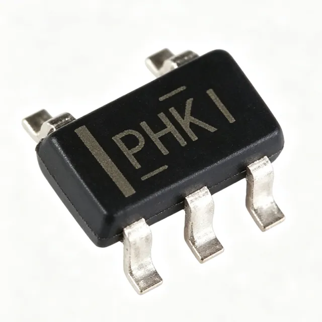
TPS62200DBVR - 300mA, 95% Buck Converter | Texas Instruments
The Texas Instruments TPS62200DBVR is a high-efficiency synchronous step-down DC-DC converter delivering up to 300 mA output current from a 5-pin SOT-23 (SOT-23-5 / SC-74A / SOT-753) package. It accepts an input voltage range of 2.5 V to 6 V and produces an adjustable output voltage from 0.7 V to 6 V, operating at a fixed 1 MHz PWM switching frequency with up to 95% efficiency. A synchronous buck converter is a type of switching voltage regulator that replaces the traditional freewheeling diode with an integrated low-side MOSFET. Within the power management IC hierarchy (converter -> switching regulator -> DC-DC converter -> power management IC), synchronous topologies achieve higher efficiency than asynchronous designs because conduction losses on the low-side switch are lower than diode forward-voltage losses, especially at light loads. Key features include up to 95% efficiency across a wide load range, 1 MHz fixed-frequency PWM operation that permits small external inductors (typically 2.2 uH) and capacitors, a 300 mA output current rating, and input compatibility with 1-cell Li-Ion, 3-cell NiMH/NiCd batteries, and standard 3.3 V or 5 V rails. The TPS6220x family also offers fixed-output voltage options, such as the TPS62205DBVR (2.5 V) and TPS62207DBVR (3.3 V), for BOM simplification. Technically, the TPS62200 integrates both power MOSFETs, the control loop, and protection features in the 5-pin SOT-23 package. The 1 MHz switching frequency reduces the required inductance and shrinks the total solution size for space-constrained portable designs. The FB pin supports precise output regulation through an external resistor divider, setting VOUT via a standard feedback network. Typical applications include powering low-voltage DSPs and microcontrollers in portable systems, battery-powered point loads in Li-Ion handheld devices, and local point-of-load conversion from 3.3 V or 5 V rails in industrial and consumer electronics. Design tip: keep the input and output ceramic capacitors (typically 4.7 uF) close to the VIN and SW pins, and choose the adjustable version only when no fixed-output variant of the TPS6220x family matches your rail voltage. This page synthesizes distributor pricing, drop-in alternatives, comparison tables, and practical design notes not found in the manufacturer datasheet.
TPS62290TDRVRQ1 - 1A 2.25MHz Automotive Buck Converter | TI
The Texas Instruments TPS62290TDRVRQ1 is a 1A synchronous step-down (buck) DC-DC converter in a 6-pin WDFN (DRV, 2x2 mm) package with an exposed thermal pad. It operates from a 2.3V to 6V input rail and delivers an adjustable output from 0.6V up to 6V at fixed 2.25 MHz switching frequency. The AEC-Q100 qualified version targets automotive point-of-load regulation requirements. A buck converter (step-down switching regulator) is a type of switched-mode power supply that uses an inductor, capacitor, and two switches (typically a high-side MOSFET and a synchronous rectifier) to efficiently convert a higher DC voltage to a lower DC voltage. By storing and releasing energy in the inductor during the switching cycle, buck converters achieve efficiency levels of 90-95%, far exceeding linear regulators that dissipate the difference as heat. The TPS62290-Q1 family belongs to TI's broader portfolio of small-package low-power PMICs that power microcontrollers, sensors, and processors in space-constrained automotive designs. Key features of the TPS62290TDRVRQ1 include up to 1A continuous output current, 2.25 MHz fixed switching frequency enabling low-noise operation and small external LC components, internal power MOSFETs, and an output voltage accuracy of 1.5%. The 2.25 MHz frequency is intentionally placed above the AM radio band to avoid EMI interference with automotive infotainment receivers. The device also supports power-save mode at light loads to extend battery life, plus internal soft-start, thermal shutdown, and over-current protection. The TPS62290TDRVRQ1 uses a voltage-mode PWM control architecture with synchronous rectification to maximize efficiency across the load range. Its internal MOSFETs and small WDFN package minimize the total solution footprint to roughly 12 mm², making it ideal for compact modules. The 2x2 mm footprint is among the smallest 1A-capable automotive regulators on the market, allowing engineers to place the converter directly adjacent to the load. Typical applications include automotive infotainment systems, Advanced Driver Assistance Systems (ADAS) sensor power, instrument clusters, body control modules, and ADAS camera/radar power rails. The wide 2.3V to 6V input supports both 3.3V and 5V automotive rails, making it drop-in compatible with most low-voltage automotive power trees. When designing with this part, keep the input capacitor within 2 mm of the PVIN pin and use a 1uH to 2.2uH inductor with low DCR. Output voltage is set by an external resistor divider on the feedback pin. Derate maximum output current at high ambient temperatures per the AEC-Q100 thermal envelope. This page synthesizes distributor pricing, drop-in alternatives, and practical design notes not found in the manufacturer datasheet alone.

TPS62355DRC - 1A 3MHz Sync Step-Down Converter | TI
The Texas Instruments TPS62355DRC is a 1 A, 3 MHz synchronous step-down DC-DC converter with an I2C-compatible interface for dynamic voltage scaling, housed in a 10-pin VSON/DFN (DRC) exposed-pad package. It accepts an input voltage range of approximately 2.7 V to 6.0 V (battery-powered portable range) and supports an adjustable output from 0.75 V (with selectable 0.9 V and 1.15 V defaults via I2C), targeting single-cell Li-ion core rails such as those feeding ARM Cortex application processors. A buck (step-down) converter is a switching regulator topology that uses an inductor and a control loop to deliver a lower output voltage from a higher input rail with high efficiency. The synchronous variant replaces the external rectifier diode with an internal low-side MOSFET, which reduces conduction loss and enables efficiencies above 88% at 3 MHz. Buck converters sit within the broader power-management IC family and are preferred over linear regulators when the input-to-output voltage difference is large, because dissipation scales with (VIN minus VOUT) times IOUT rather than VIN. Key features of the TPS62355DRC include a 3 MHz fixed switching frequency, best-in-class load and line transient response, a complete 1 mm component profile solution that enables ultra-thin PCB designs, and ±2 percent PWM DC voltage accuracy. The I2C-compatible interface allows the system processor to reprogram VOUT on the fly for dynamic voltage scaling, a critical technique for extending battery life in smartphones, wearables, and other portable devices. Architecturally, the device integrates high-side and low-side MOSFETs in a single die, eliminating the external rectifier and shrinking the overall solution to roughly 4 mm x 5 mm. The 3 MHz switching frequency allows the use of a 1 uH inductor and tiny ceramic output capacitors, and the exposed thermal pad keeps junction temperature low even under full 1 A load. Typical applications include single-cell Li-ion powered portable electronics such as smartphones, tablet computers, and wearable devices, as well as USB-powered peripherals, Bluetooth headsets, and low-power FPGAs requiring small-footprint core rails. The I2C programmability makes it especially attractive in dynamic voltage scaling (DVS) schemes where the application processor reduces its supply voltage during idle periods to minimize battery drain. When designing with this part, prioritize a tight, low-ESR ceramic output capacitor placed within 1 mm of the DRC pad and follow the recommended 1 uH chip inductor with less than 50 mohm DCR for peak efficiency. Designers should also budget the I2C pull-ups for 400 kHz Fast-Mode operation when system response time matters. This page synthesizes distributor pricing, drop-in alternatives, and practical design notes not found in the manufacturer datasheet.
TPS62590DRVR - 2.25MHz 1A Step-Down Converter | Texas Instruments
The Texas Instruments TPS62590DRVR is a high-efficiency synchronous step-down (buck) converter optimized for battery-powered portable applications. It delivers up to 1A output current from a single Li-Ion cell or 2-3 AA/AAA batteries, with an input voltage range of 2.5V to 5.5V. The device is available in a compact 6-pin WSON (2mm x 2mm) package with exposed thermal pad, making it ideal for space-constrained designs. A step-down converter, also known as a buck converter, is a type of DC-DC switching regulator that steps down an input voltage to a lower output voltage with high efficiency. Unlike linear regulators, which dissipate excess power as heat, switching regulators use inductive energy storage to achieve efficiencies often above 90%, making them essential in battery-powered devices where power conservation is critical. The TPS62590 belongs to the family of synchronous buck converters, which use an internal high-side and low-side MOSFET to avoid the need for an external Schottky diode, further improving efficiency. Key features of the TPS62590DRVR include a 2.25MHz fixed switching frequency, which allows the use of small, low-cost inductors and capacitors, reducing PCB footprint. The output voltage is adjustable from 0.75V to 5.5V via an external resistor divider, with an accuracy of ±2.5% in PWM mode. The device supports 100% duty cycle operation for lowest dropout, and features a low quiescent current of 15µA (typical), extending battery life in light-load conditions. It also includes internal soft-start, overcurrent protection, and thermal shutdown. Technically, the TPS62590 uses a current-mode control architecture with synchronous rectification, providing fast transient response and stable operation with ceramic output capacitors. The 2.25MHz switching frequency is above the AM radio band, reducing EMI concerns. The device operates over a junction temperature range of -40°C to +125°C, with an ambient temperature range of -40°C to +85°C. Typical applications include powering DSPs, microcontrollers, and FPGAs in portable devices, as well as point-of-load (POL) converters in battery-powered equipment such as smartphones, tablets, and wireless sensors. Its high efficiency and small size make it particularly suitable for wearable devices and IoT nodes. When designing with the TPS62590DRVR, ensure proper input and output capacitor selection (typically 10µF input and 22µF output) and place them close to the IC. The exposed pad should be soldered to a large copper area for thermal management. The feedback resistor divider should use 1% tolerance resistors to maintain output accuracy.
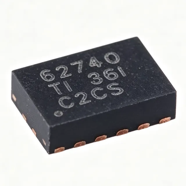
TPS62740DSSR - 300mA 360nA Iq Buck Converter | Texas Instruments
The Texas Instruments TPS62740DSSR is an ultra-low-power step-down buck DC-DC converter delivering up to 300mA output current from a 2.2V to 5.5V input, housed in a compact 12-pin 2x3mm WSON (DSS) package with exposed pad. It is purpose-built for battery-powered Bluetooth Low Energy (BLE) and wireless sensor applications, featuring a typical quiescent current of only 360nA. A step-down (buck) converter is a switching voltage regulator that efficiently converts a higher input voltage to a lower output voltage using a switch, inductor, and capacitor. Within the power management IC hierarchy, it belongs to the DC-DC converter family, which achieves far higher efficiency than linear regulators by storing and transferring energy rather than dissipating it as heat. This makes buck converters the preferred choice for extending battery life in portable and IoT systems. Key features include up to 90% efficiency at just 10uA output current, RF-friendly DCS-Control topology, and a switching frequency of up to 2MHz, which permits a tiny 2.2uH inductor and 10uF output capacitor for a total solution size of approximately 31mm2. The device also integrates a load switch, enabling system power gating of downstream circuitry to further reduce standby current. The DCS-Control (Direct Control with Seamless Transition into Power Save Mode) architecture combines the low output ripple of PWM operation with the high light-load efficiency of PFM power-save mode, transitioning seamlessly without transient excursions. This is critical for RF power rails, where ripple and spurious noise can degrade transmitter phase noise and receiver sensitivity. Compared with conventional power-save-mode converters, the seamless transition means output impedance stays low across the entire load range, preserving output-voltage accuracy from full load down to nanoamp quiescent levels. Typical applications include BLE beacons and sensors, energy harvesting systems, wearable devices, and battery-powered metering, where a single lithium or alkaline cell must power the system for months or years. With 360nA quiescent current, a coin cell (approx. 220mAh) can support a duty-cycled sensor node for several years in standby-dominated operation. Design consideration: optimize the output capacitor ESR and inductor value per the TI datasheet recommendation (2.2uH, 10uF) to preserve the low-ripple, RF-friendly behavior in power-save mode. This page synthesizes distributor pricing, drop-in alternatives, and practical design notes not found in the manufacturer datasheet.
TPS62745DSSR - 300mA Ultra-Low IQ Step-Down Converter | Texas Instruments
The Texas Instruments TPS62745DSSR is a 300 mA ultra-low quiescent-current synchronous step-down (buck) DC/DC converter housed in a 12-pin WSON (DSS) package with exposed thermal pad. It accepts a 3.3 V to 10 V input range and delivers a programmable output voltage of 1.8 V to 3.3 V via the VSEL pin, while achieving typically 360 nA quiescent current for sleep-mode efficiency in battery-powered applications. The device is targeted at low-power wireless systems that must ride through long idle periods on small cells such as CR2032, 2xAA, or Li-ion batteries. What is a step-down (buck) DC/DC converter? A buck converter is a switched-mode power supply (SMPS) topology that converts a higher input voltage to a lower regulated output voltage by storing energy in an inductor and switching it through synchronous MOSFETs at high frequency. Buck converters sit within the broader hierarchy of voltage regulators -> power management ICs -> semiconductors. Compared with linear regulators (LDOs), buck converters trade a small switching-ripple penalty for 80-95% efficiency across a wide VIN/VOUT differential, making them essential when battery energy is precious. Key features of the TPS62745DSSR include a sub-1 uA quiescent current, integrated MOSFETs (no external power switches), VSEL output-voltage switching for dynamic power-rail selection, and an input-voltage switch (VIN_SW) that lets the device ride through supply transients. Output current is rated to 300 mA continuous, with a 2.5 MHz typical switching frequency that allows the use of a tiny 1.0 uH inductor and small ceramic capacitors, minimising total solution footprint. The TPS62745DSSR uses TI's DCS-Control topology (Direct Control with Seamless transition into power-saving mode) to maintain high efficiency across the entire 1 mA to 300 mA load range. A dedicated power-good output, internal soft-start, and thermal shutdown protection complete the integration. The WSON-12 exposed-pad package offers a low thermal resistance path, supporting operation from -40 C to +125 C junction temperature. Typical applications include Bluetooth Low Energy (BLE) sensor nodes, wearable health monitors, energy-harvesting power conditioning, smart thermostats, and IoT endpoint devices powered by coin-cell or dual-AA batteries. The ultra-low IQ and high light-load efficiency directly extend battery life when radio duty-cycling dominates the average current draw. When designing with this part, select the inductor for both DC resistance and saturation current rating at peak load, and place the input/output ceramic bypass capacitors within 2 mm of the package to keep the feedback loop stable. Verify that the VSEL logic levels match the host MCU's GPIO rail before relying on dynamic voltage scaling. This page synthesises distributor pricing, drop-in WSON-12 alternatives, and practical low-power design notes that are not consolidated in the manufacturer datasheet, giving engineers a faster path from selection to qualified BOM.
TPS62810QWRWYRQ1 - 4A Automotive Buck Converter | TI
The Texas Instruments TPS62810QWRWYRQ1 is an automotive-grade synchronous step-down DC/DC converter delivering up to 4A of continuous output current from a 2.75V to 6V input, with an adjustable output voltage starting from 0.6V. It is housed in a compact 2mm x 3mm VQFN-9 (RWY) package with wettable flanks for enhanced solder-joint inspection in automotive manufacturing. A synchronous buck converter is a type of switching voltage regulator that steps down a higher input voltage to a lower output voltage with high efficiency, typically above 90%. Within the power management IC hierarchy, buck converters sit alongside LDOs and boost converters and are preferred whenever load current or efficiency demands exceed what a linear regulator can dissipate. The TPS62810QWRWYRQ1 belongs to the TPS6281x-Q1 family of pin-to-pin 1A, 2A, 3A, and 4A automotive converters. Key features include AEC-Q100 qualification (temperature grade 1, -40C to +125C ambient), Functional Safety-Capable documentation to support ISO 26262 system design, and peak current mode control topology for fast transient response. Low-resistive integrated switches minimize conduction losses, while the adjustable switching frequency can be synchronized to an external clock to control EMI. A power-good output, enable pin, and soft-start support robust power sequencing in multi-rail systems. The device is designed for automotive applications such as infotainment and advanced driver assistance systems (ADAS). Reference designs pair the TPS62810-Q1 with an LM63635-Q1 bus converter switching at 2.1 MHz, with the load converters switching at 2.2 MHz to ease filtering. Typical rails include core supplies for processors, camera and radar modules, and communication modules in vehicles. When designing with this converter, choose input and output capacitors and the inductor per the datasheet guidelines to maintain stability and minimize output ripple. Use thermal vias under the exposed pad to optimize heat dissipation at full 4A load.
TPS62811QWRWYRQ1 - 1A 6V Automotive Step-Down Buck | TI
The Texas Instruments TPS62811QWRWYRQ1 is an AEC-Q100 qualified automotive 2.75-V to 6-V input, 1-A step-down (buck) switching regulator with adjustable output voltage starting at 0.6 V, housed in a 2 mm x 3 mm 9-pin wettable-flank QFN (RWY/QFN-HR) package. A step-down converter, also called a buck converter, is a type of DC-DC switching regulator that converts a higher input voltage to a lower output voltage with high efficiency by rapidly switching an internal power stage and filtering the result through an inductor and capacitor. Buck converters sit within the power management IC hierarchy (voltage regulator -> switching regulator -> DC-DC converter) and are the workhorses of point-of-load power conversion in automotive and industrial systems, where they routinely exceed 90% efficiency compared with 40-60% for linear regulators. Key features of the TPS62811QWRWYRQ1 include a wide 2.75 V to 6 V input range that directly supports automotive 5-V and 3.3-V rails and cold-crank-tolerant pre-regulator outputs, a 1-A continuous output current rating, adjustable output voltage from 0.6 V, and adjustable-frequency operation that lets designers trade switching loss against passive-component size. The wettable-flank QFN package enables reliable solder-joint inspection (AOI) required in automotive manufacturing. Architecturally, the device belongs to the TPS6281x-Q1 family, which shares the DCS-Control style control topology known for fast, stable transient response with small output capacitance; the datasheet details compensation settings and output-capacitor ranges (for example, minimum capacitance values rising for outputs below 1 V on related family members such as TPS62810-Q1 and TPS62813-Q1). Typical applications include automotive ADAS camera and sensor module point-of-load rails, infotainment and cluster supplies fed from 5-V rails, and industrial systems requiring AEC-Q100 Grade 1 robustness at -40C to +125C ambient. Design consideration: because this is a switching regulator, PCB layout matters - keep the input capacitor, inductor, and SW/GND loops tight and place feedback traces away from the switch node for best output ripple and stability. This page adds value beyond the TI datasheet by synthesizing distributor pricing, drop-in family alternatives, design notes, and AEO-optimized FAQ content in one place. Pricing reflects data as of 2026-10-13.
TPS62825DMQR - 2A Step-Down Converter 2.4-5.5V | Texas Instruments
The Texas Instruments TPS62825DMQR is a 2-A synchronous step-down (buck) DC/DC converter with 2.4-V to 5.5-V input range, 1% output voltage accuracy, and adjustable output down to 0.6 V, packaged in a 6-pin VSON-HR (DMQ) 1.5-mm x 1.5-mm module. The device uses TI's DCS-Control topology to deliver fast transient response and operates at a typical switching frequency of 2.2 MHz, enabling a very small 470 nH inductor, a single 4.7 µF input capacitor, and only one 22 µF (or two 10 µF) output capacitors. A step-down converter (also called a buck converter) is a switch-mode DC/DC regulator that converts a higher input voltage to a lower output voltage with high efficiency by rapidly switching an inductor and rectifying the resulting waveform. As a member of the broader DC/DC converter family, it sits hierarchically under switching regulators, then voltage regulators, then power management ICs. This category is essential in modern battery-powered and space-constrained electronics because linear regulators waste VIN-VOUT * IOUT as heat, whereas a properly designed buck like the TPS62825 typically achieves 90%+ efficiency across most of its load range. Key features of the TPS62825DMQR include a best-in-class quiescent current of 4 µA (light-load), 2-A continuous output current, 2.4-V to 5.5-V input voltage range, output voltage adjustable from 0.6 V up to 4 V, 2.2-MHz fixed switching frequency, power-good output, and an enable pin that supports power sequencing. The device supports both forced PWM and power-save (DCM) operation, optimizing efficiency at light loads. The DCS-Control (Direct Control with Seamless transition into power-save mode) architecture combines the fast transient response of hysteretic control with the high efficiency of a pulse-frequency-modulated (PFM) light-load mode. The internal reference is trimmed to 1% accuracy over the -40 °C to +125 °C junction-temperature range, providing a tight output tolerance demanded by core-rail and SoC power requirements. Typical applications include powering processors, FPGAs, and SoCs from a single-cell Li-ion battery, 5-V USB rails, low-power IoT sensors, portable consumer devices, and wearable electronics. The wide VIN range also makes the part suitable for 3.3-V industrial bus rails. When designing with the TPS62825DMQR, place the input 4.7-µF ceramic and the 470-nH inductor as close to the IC as possible, return all grounds to a single low-impedance exposed pad, and select the feedback resistors so the output lands within the 0.6-V to 4-V regulation window. With its 2-A rating and compact 1.5-mm x 1.5-mm QFN, it minimizes both PCB area and BOM cost. This page synthesizes distributor pricing, same-family and cross-brand drop-in alternatives, and practical design notes that go beyond the manufacturer datasheet.
TPS62827ADMQR - 4A Buck Converter 2.4-5.5V Input | TI QFN-6
The Texas Instruments TPS62827ADMQR is a 4-A synchronous step-down DC/DC converter with an input voltage range of 2.4 V to 5.5 V and a 1% accurate adjustable output from 0.6 V up to the input rail, packaged in a compact 6-pin 1.5 mm x 1.5 mm VSON-HR (QFN) module. The part uses TI's DCS-Control (Direct Control with Seamless transition) topology, achieving a quiescent current of only 4 uA while delivering fast transient response for dynamic load steps typical of portable processors. A buck converter (step-down switching regulator) is a type of DC-DC converter that efficiently reduces a higher DC input voltage to a lower DC output voltage. Within the power-management hierarchy, the TPS62827ADMQR sits between the battery/USB rail and the point-of-load. It belongs to the DC-DC converter family, which itself is a sub-category of power management ICs in the broader semiconductor ecosystem. The DCS-Control architecture combines hysteretic and PWM control, eliminating the need for external compensation components and enabling a tiny external BOM. Key differentiators include the 4 uA quiescent current for long battery standby, 1% output accuracy across the -40 C to +125 C junction range, true 4-A continuous output current in a 6-pin 1.5 mm x 1.5 mm package, internal MOSFETs (no external FETs), and support for forced-PWM, power-save, and ultrasonic modes. The device is pin-to-pin and BOM-to-BOM compatible with the rest of the TPS6282x family, allowing 1/2/3/4-A current scaling on a single PCB layout. Typical applications include 1-cell Li-ion / 2-cell alkaline battery-powered systems, USB Type-C powered accessories, solid-state drives, portable consumer electronics, and infotainment head units. The wide 2.4 V to 5.5 V input range lets a single device operate from a depleted Li-ion cell (2.5 V) all the way through USB VBUS (5 V) without a pre-regulator. When designing with this device, choose a 470 nH inductor and place input/output capacitors within 1 mm of the exposed thermal pad; the pad MUST be soldered to a top-layer copper pour to carry 4 A dissipation in still air. Always check the derating curves in the manufacturer datasheet to ensure the junction temperature stays below 125 C at worst-case load.
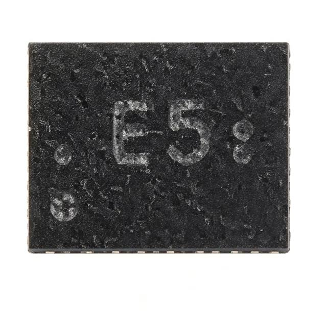
TPS62840DLCR - 60nA IQ 750mA Buck Converter 1.8-6.5V | TI
The Texas Instruments TPS62840DLCR is a high-efficiency step-down (buck) converter that operates from a 1.8 V to 6.5 V input rail and delivers up to 750 mA of output current from an 8-pin VFDFN (DLC) package measuring 3.0 mm x 3.0 mm. Its headline specifications are an ultra-low 60 nA typical quiescent current, 1.8 MHz nominal switching frequency, and 750 mA continuous output capability. The DCR suffix indicates the VFDFN-8 package orientation qualified for the industrial -40C to +125C junction range, and the R suffix on DLC indicates tape and reel packaging. A buck converter (also called step-down converter) is a switching-mode DC-DC regulator that converts a higher input voltage to a lower output voltage by rapidly switching an inductor and rectifying the stored energy. Within the broader taxonomy, a buck converter sits as a sub-type of DC-DC converter, which belongs to the family of voltage regulators, which itself is a category of power management integrated circuits (ICs). Buck converters are the dominant topology for battery-powered electronics because they achieve efficiencies of 80-95%, far higher than the linear regulators (LDOs) they often replace. Key features include the 120 nA IQ achieved in 100% duty-cycle mode for end-of-discharge battery operation, DCS-Control topology that combines voltage-mode and current-mode control for clean RF powering, a STOP pin that disables switching during noise-sensitive measurements, and Power Save Mode that reduces switching frequency at light load to maintain efficiency. The 1.8 MHz switching frequency allows small external inductors and ceramic-only capacitors, enabling a complete sub-1 cm-squared solution footprint. The output voltage is adjustable via an external resistor divider. Technically, the TPS62840 integrates high-side and low-side MOSFETs, a precision reference, and a programmable soft-start. Integrated protection features include overcurrent protection, thermal shutdown, and undervoltage lockout. The wide 1.8 V to 6.5 V input range supports 2S-4S alkaline (2-6 V), 1S-2S Li-MnO2 (3-6 V), 1S Li-Ion/Li-Polymer (2.7-4.2 V), and energy harvester outputs up to 6.5 V. The combination of low IQ and high peak-load capability makes the device especially well suited to IoT duty-cycled loads where sleep currents dominate the energy budget. Typical applications include battery-powered IoT sensors, wearables and wireless earbuds, smart utility meters, energy-harvesting sensor nodes, and standby rails for microcontrollers. It is also used to power RF transceivers (BLE, LoRa, sub-GHz) in wireless sensor nodes and as an auxiliary rail in portable medical and industrial monitor designs. Design tip: place 10 uF input and 22 uF output ceramic capacitors within 2 mm of the IC, choose a 1.8 MHz-rated inductor in the 1-2.2 uH range, and use the STOP pin in test and measurement setups to eliminate switching ripple during ADC acquisition windows. This page synthesizes distributor stock, pricing tiers, drop-in alternatives, and practical design notes that complement the TI datasheet and help engineers select and qualify the TPS62840DLCR for always-on battery applications.
TPS62841DLCR - 750mA, 60nA IQ Step-Down Converter | Texas Instruments
The Texas Instruments TPS62841DLCR is a high-efficiency synchronous step-down (buck) DC-DC converter with an ultra-low quiescent current of typically 60 nA, delivering up to 750 mA output current from a 1.8 V to 6.5 V input rail, housed in an 8-pin VFDFN (DLC) package. It uses DCS-Control topology with a typical switching frequency of 1.8 MHz, supporting small inductors and capacitors for compact IoT and wearable designs. The output voltage is adjustable down to 0.8 V, making it suitable for powering modern processors, MCUs, and radios from single-cell Li-ion or multi-cell alkaline sources. A step-down (buck) converter is a type of switched-mode power supply (SMPS) that efficiently steps a higher DC input voltage down to a lower DC output voltage by rapidly switching an inductor/capacitor energy-transfer network. Within the broader power management taxonomy, a buck converter sits under DC-DC converters, alongside boost, buck-boost, and LDO topologies. Compared with linear regulators, buck converters achieve much higher efficiency (often above 90%) at the cost of higher output ripple and switching noise; LDOs trade efficiency for ultra-clean output. The TPS62841 family targets the ultra-low-IQ segment where standby drain dominates total energy budget. Key features include 60 nA typical quiescent current (120 nA in 100% mode), 750 mA continuous output current, an operating input range of 1.8 V to 6.5 V, and an adjustable output from 0.8 V upward via an external resistor divider. Power-Save Mode maximizes light-load efficiency, while DCS-Control provides clean PWM operation at higher loads. Integrated MOSFETs and internal compensation reduce external component count to one inductor plus input/output capacitors. The TPS62841DLCR achieves peak efficiency above 90% at moderate loads and supports DCS-Control to cleanly power noise-sensitive radio blocks. Its 1.8 MHz typical switching frequency keeps the fundamental and harmonics well above the AM band, simplifying EMI filtering in space-constrained designs. Typical applications include battery-powered IoT sensors, wearable health monitors, Bluetooth/Zigbee/LoRa nodes, energy-harvesting systems, and always-on microcontroller rails. The wide input range also supports USB and 2x AA/AAA alkaline source designs where quiescent drain directly determines operating life. When designing with the TPS62841DLCR, ensure the inductor saturation current exceeds the peak switch current and that the input/output ceramic capacitors meet the datasheet's minimum effective capacitance after DC bias derating. Power-Save Mode is automatic, but the converter exits PFM at heavy load and re-enters cleanly; leave adequate copper for thermal relief of the exposed pad. This page synthesizes distributor pricing, drop-in alternatives, application guidance, and design notes that complement - rather than duplicate - the official Texas Instruments datasheet.
TPS628502QDRLRQ1 - 2A Automotive Buck Converter 2.7V-6V | TI
The Texas Instruments TPS628502QDRLRQ1 is a 2-A continuous-output automotive synchronous step-down (buck) DC/DC converter housed in an 8-pin SOT-583 (DRL) package. Operating from a 2.7-V to 6-V input rail, the device delivers up to 2 A of continuous load current (3 A peak capability shared across the TPS62850x-Q1 family) at switching frequencies up to 4 MHz, making it suitable for space-constrained automotive point-of-load applications. The AEC-Q100-qualified converter is part of TI's pin-to-pin compatible TPS62850x-Q1 family that scales across 1 A, 2 A, and 3 A peak load levels for hardware reuse across multiple rails. A buck converter (step-down switching regulator) is a type of DC-DC converter that uses an inductor and switching elements to convert a higher DC input voltage into a lower regulated DC output voltage at high efficiency. It belongs to the power management IC (PMIC) hierarchy and is preferred over linear regulators when the input-to-output voltage differential is large, because it dissipates far less power as heat. Synchronous buck converters integrate both the high-side and low-side MOSFETs, removing the need for an external Schottky diode and improving efficiency at low output voltages. Key features include a peak current-mode control topology for fast transient response, a MODE/SYNC pin that accepts an external clock for frequency synchronization or selects forced-PWM versus auto-PWM operation, and a wide Vin range that simplifies designs powered from 3.3-V or 5-V rails or directly from automotive battery transients. The SOT-583 footprint (approximately 1.6 mm x 1.6 mm) keeps the solution area compact, and the 4-MHz switching frequency enables the use of small inductors and ceramic output capacitors. Typical automotive applications include ADAS sensor power rails, infotainment processors, body electronics modules, and rear-view camera supplies. The device also suits industrial point-of-load conversion and any 5-V distributed-bus system that needs high efficiency in a small area. When designing with this part, follow the datasheet's minimum on-time and minimum off-time limits carefully when setting the external frequency-adjust resistor; violating these can degrade regulation. Add input ceramic capacitors close to the PGND and VIN pins to minimize ringing and EMI. This page synthesizes distributor pricing, drop-in pin-compatible alternatives, comparison data, and practical design notes that complement the manufacturer datasheet and accelerate component selection.
TPS628660AYCGR - 6A Sync Buck Converter, 5.5V, I2C | TI
The Texas Instruments TPS628660AYCGR is a 6 A synchronous step-down (buck) DC-DC converter with I2C interface, housed in a compact 15-pin XFBGA/WCSP (DSBGA, package code YCG) measuring 1.05 mm x 1.78 mm x 0.5 mm. It accepts an input voltage range of 2.4 V to 5.5 V and provides an adjustable output from 0.4 V up to roughly 1.55 x VIN (up to about 4 V in typical use), making it ideal for point-of-load conversion in space-constrained portable and IoT systems. A buck (step-down) DC-DC converter is a switching-mode power supply circuit that uses an inductor and two switches (typically MOSFETs) to convert a higher DC input voltage into a lower DC output voltage with high efficiency. As a member of the synchronous buck family of voltage regulators (DC-DC converter -> switching regulator -> power management IC -> semiconductor), the TPS62866 family operates at high switching frequency to minimize external LC component size, enabling a sub-2 mm solution footprint suitable for wearable, smartphone, and battery-powered applications. Key technical features include 7 mΩ and 6.5 mΩ internal power MOSFETs, I2C-compatible interface up to 3.4 Mbps for output voltage scaling and telemetry, a VID pin for dynamic voltage scaling (DVS), power-good indication, and thermal pre-warning plus thermal shutdown protection. The high switching frequency supports tiny inductors and capacitors, achieving a solution height of less than 1 mm. The TPS628660AYCGR uses adaptive on-time control architecture with internal compensation, simplifying external design while delivering fast transient response to load steps. The I2C interface allows output voltage margining and monitoring without external resistor changes, while the VID pin enables hardware-based dynamic voltage scaling - critical for processors that lower core voltage in idle states to extend battery life. Typical applications include powering processors, FPGAs, and SoCs in mobile devices, IoT sensor nodes, wearables, single-cell Li-ion battery powered systems, and portable industrial instruments. Its small footprint and I2C programmability suit designs that require adaptive power management under varying load conditions. When designing with this device, place input capacitors as close as possible to the PVIN pin to reduce switching noise. Maintain the PGND-to-AGND ground separation recommended in the datasheet to avoid ground bounce, and use the I2C pins with a pull-up resistor on the host side. Verify that the chosen inductor's saturation current exceeds the device's peak current limit for reliable operation. This page synthesizes distributor pricing, real-world pin-compatible TI alternatives in the same YCG WCSP footprint, and practical design notes that go beyond the manufacturer datasheet.

TPS6287B20VA0WRZVR - 20A Sync Buck Converter | Texas Instruments
The Texas Instruments TPS6287B20VA0WRZVR is a 20A synchronous step-down DC/DC buck converter with I2C interface and differential remote sense, operating from a 2.7V to 6V input and delivering a programmable 0.4V to 1.675V output in a 24-pin WQFN (RZV) package with exposed pad. A buck (step-down) converter is a switching voltage regulator that efficiently reduces a higher DC input voltage to a lower, tightly regulated output voltage using high-frequency switching of integrated power MOSFETs together with an inductor and capacitors. Within the power-management IC hierarchy, it belongs to the family of switching regulators, which achieve far higher efficiency than linear regulators (LDOs), making them the default choice for high-current point-of-load supplies in modern digital systems. Key features include a pin-to-pin compatible current family spanning 10A (TPS6287B10), 15A (B15), 20A (B20), 25A (B25) and 30A (B30), three selectable output voltage ranges with output resolution down to 1.25mV steps, low-resistance integrated power switches for high efficiency at high ambient temperature, and stacking support in parallel mode for even higher output currents. The TPS6287B20 architecture emphasizes fast transient response: it is specified as a fast-transient synchronous converter, allowing tight voltage regulation on dynamically loading rails such as processor cores and FPGAs. The I2C interface enables output voltage programming, telemetry, and status monitoring, while the differential remote sense input compensates for PCB voltage drop at the point of load. Frequency synchronization is also supported, simplifying multi-rail EMI management. Typical applications include powering high-current SoC and FPGA core rails, network processors and switch ASICs, data-center storage and server point-of-load supplies, and stacking multiple devices for 40A-plus rails in AI accelerators and high-performance computing. Design consideration: because this is a high-current buck regulator, inductor selection, switch-node layout, and thermal copper area dominate performance - follow the Texas Instruments datasheet layout guidelines closely to minimize switching losses and board-level temperature rise. This page synthesizes distributor pricing, pin-to-pin family alternatives, drop-in options, and practical design notes not found in the manufacturer datasheet alone.