Logic ICs
بەرهەمەکان (720+)

DP8341N - Bipolar Decoder Receiver 24-DIP | National
The National Semiconductor DP8341N is a bipolar decoder/receiver integrated circuit supplied in a 24-pin PDIP package. The verified distributor records identify it as an MPU circuit, bipolar decoder and receiver, with RoHS-compliant status reported by IC Online. Its core role is to receive and decode digital bus information within older microprocessor-compatible systems. What is a decoder/receiver integrated circuit? A decoder/receiver is a specialized logic IC that accepts encoded or serial digital information and converts it into decoded control or data signals. It belongs to the broader logic IC and decoder/receiver hierarchy, sitting between a digital bus or communication line and the control logic of a microprocessor-based system. Such devices commonly support older bus architectures where signal direction, voltage levels, and timing must be translated into usable digital outputs. The verified information establishes a bipolar 24-DIP package and decoder/receiver classification, but does not provide detailed electrical timing, supply-voltage, output-current, or pin-function data. Consequently, those values must be confirmed against the original manufacturer documentation before designing a new circuit or substituting the device. The package is a through-hole PDIP-24 format, making it suited to legacy controller cards, industrial control equipment, and repair or maintenance platforms that retain compatible sockets. Typical design use includes legacy microprocessor interface boards, bus decoding, signal-conditioning subsystems, and industrial control systems built around older bipolar logic. Because the available records call the DP8341N a specialized decoder/receiver, system compatibility should be established from the original pinout, supply requirements, logic levels, and timing behavior. Those parameters are not present in the supplied verified data and are therefore not inferred here. The DIP-24 package should be handled with standard electrostatic-discharge precautions and installed according to the original package orientation. Do not substitute a mechanically similar decoder solely by its DIP package count; verify every pin, voltage level, timing parameter, and power connection before substitution. This distinction is important because package compatibility alone does not establish functional compatibility. This product page consolidates verified distributor listings, package identification, manufacturer identity, and sourcing context while explicitly separating unavailable technical details. It is intended to support initial sourcing and legacy-system investigation, with final electrical validation delegated to the original National Semiconductor datasheet or an authorized technical reference.

DS28E25+ - SHA-256 1-Wire Authenticator, 4Kb EEPROM, TO-92 | Analog Devices
The Analog Devices DS28E25+ (formerly Maxim Integrated) is a DeepCover secure authenticator that combines a hardware SHA-256 accelerator, a 4096-bit user EEPROM, and a unique 64-bit ROM ID on a single 1-Wire bus in a TO-92 (3-pin) through-hole package. It operates from 2.97 V to 3.63 V on the data/parasite-power line and communicates over the single-contact 1-Wire interface at standard and overdrive speeds, providing strong cryptographic authentication for anti-counterfeiting and peripheral identification. A secure authenticator is a specialized IC category within the broader semiconductor security hierarchy: secure authenticator -> cryptography IC -> security IC -> interface/specialized IC. DeepCover is Analog Devices' portfolio of security ICs that embed cryptographic primitives, physically secure key storage, and active die-level shielding to protect against invasive and non-invasive attacks, addressing system-on-board (SoB) and peripheral-authentication use cases where a software-only root-of-trust is insufficient. Key features include hardware SHA-256 computation over user memory, a 64-bit secret, a host random challenge, and the 64-bit ROM ID; on-chip 4 Kb (512-byte) user EEPROM organized in 32 pages of 16 bytes; 1-Wire overdrive communication up to 76.9 kbps; a unique factory-lasered 64-bit registration number; and write-only/read-only protection modes per page. The TO-92 package is chosen for cable-mounted peripherals (medical sensors, printer cartridges, e-meter modules) where the authenticator is soldered or clipped onto a flying lead and survives harsh mechanical environments. Architecturally, the DS28E25 isolates the secret in a protected memory block that participates in the SHA-256 hash but is never exposed on the bus. Host-side verification reads the public EEPROM, generates a random challenge, computes SHA-256 in firmware, and compares the result with the device-returned MAC - a strong two-factor scheme where knowledge of the secret alone cannot impersonate the device without the physical silicon. Typical applications include medical sensor authentication (single-use disposable probes), printer and consumable cartridge identification, industrial control module anti-counterfeiting, e-meter tamper detection, and IoT node provisioning. In each case the DS28E25+ provides a hardware root-of-trust that is impractical to clone. When designing with this part, place a strong pull-up (typically 4.7 kohm to VPUP, the 1-Wire pull-up rail) on the data line, observe the VPUP range of 2.97 V to 3.63 V during reads and EEPROM writes, and verify parasitic-power budgeting during long EEPROM-programming intervals where current can reach several milliamps. Decoupling on the VPUP rail with a 0.01 uF to 0.1 uF ceramic capacitor close to the device improves write reliability. This page synthesizes distributor pricing, drop-in alternatives from the same product family and competitor equivalents, and practical design notes not found in the manufacturer datasheet.

DS90CP02SP - 1.5Gbps 2x2 LVDS Crosspoint Switch | Texas Instruments
The Texas Instruments DS90CP02SP is a 1.5-Gbps 2x2 LVDS crosspoint switch with one function and two channels, designed for high-speed signal routing over lossy FR-4 printed-circuit-board backplanes and balanced cables. Its fully differential signal paths support signal integrity and noise immunity, while the non-blocking architecture allows any input to connect to either output. The device is supplied in a 28-UQFN package measuring 5 mm by 5 mm. A crosspoint switch is a signal-routing IC that directs data from multiple inputs to multiple outputs under control of external logic. In the broader electronics hierarchy, a crosspoint switch belongs to logic ICs and multiplexing or switching circuits. The DS90CP02SP is specialized for differential LVDS links rather than ordinary single-ended digital signals. Its architecture is intended to preserve data integrity across long or electrically demanding interconnect paths, including backplanes and balanced cables. The principal verified feature is its 1.5-Gbps data rate for a 2x2 LVDS crosspoint configuration. The two-channel architecture supports routing flexibility in systems that need selectable signal paths. The non-blocking operation permits simultaneous routing options without forcing a fixed point-to-point mapping. Fully differential paths help reject common-mode noise and maintain signal polarity through controlled differential signaling. The package is identified by distributors as 28-UQFN, with a 5 mm by 5 mm body. The device is targeted at high-speed communications and signal-integrity-sensitive routing. Its differential signal paths can be used when a system must connect source and destination circuitry through a controlled crosspoint rather than a fixed trace. The wide input common-mode capability is identified in the manufacturer description as useful for practical LVDS interoperability, although detailed input thresholds, output levels, timing, power ratings, and temperature limits are not included in the supplied verified data. Typical applications include LVDS backplane routing, balanced-cable signal switching, industrial control links, communications equipment, and test systems where a compact differential routing element is useful. The same 28-UQFN footprint should be used as the mechanical starting point for PCB layout. The exact pin assignments, recommended resistor networks, trace geometry, and power-decoupling requirements must be confirmed from the official Texas Instruments datasheet before implementation. A key design consideration is that high-speed differential routing depends as much on PCB layout as on the switch itself. Keep each differential pair tightly matched, minimize stubs, maintain continuous reference planes, and control impedance through the backplane or cable transition. Verify the complete channel with the intended source and destination devices because transmitter amplitude, receiver thresholds, connector geometry, and loss characteristics determine the usable system margin. This product record combines the verified Texas Instruments device description with distributor package and channel information, a structured application view, and engineering guidance focused on LVDS signal integrity. It is intended to support early design decisions while leaving unverified electrical details explicitly marked for confirmation against the official datasheet.

DS90LV110ATMTX - 1:10 200MHz LVDS Clock Distributor | TI
The Texas Instruments DS90LV110ATMTX is a 1-to-10 LVDS data and clock distributor with failsafe operation, a maximum clock frequency of 200 MHz, and a 28-pin TSSOP package. Designed for point-to-point clock distribution, the device accepts one differential input and provides ten differential outputs. It supports 3.3 V operation, LVDS signaling, and output tri-state control through an enable input, making it suitable for timing-heavy backplanes, telecommunications equipment, industrial controls, and test systems. An LVDS clock distributor is a low-voltage differential signaling interface device that regenerates and distributes a high-speed differential clock across multiple receivers. Its place in the signal-chain hierarchy is clock and timing IC, then clock buffer or driver, then interface logic and semiconductor. Differential signaling reduces sensitivity to common-mode noise, while low swing levels support reliable high-speed data transmission over controlled-impedance printed circuit boards. The principal features of the DS90LV110ATMTX include ten true outputs, a 200 MHz maximum clock frequency, a 3.9 ns propagation delay, and support for LVDS, CML, and PECL-compatible signaling described for the device. The outputs can enter a high-impedance state through the enable function. Its -40°C to +85°C industrial temperature range supports commercial and industrial equipment, while the gull-wing TSSOP-28 package provides a conventional surface-mount footprint. The one-input, ten-output topology is important in clock-tree design because it allows a single low-skew source to feed multiple destinations without requiring ten separate buffers. The 400 Mb/s signaling rate and 0.45 V differential output level align the device with low-voltage differential clock and data networks. The failsafe behavior helps define the output state when the input is missing or invalid, helping downstream receivers avoid operating on undefined data. Typical applications include central clock distribution for telecommunications line cards, synchronized operation across industrial control modules, fanout for backplane endpoints, laboratory instrumentation, and clocking for high-speed interface subsystems. In each case, controlled-impedance routing, matched pair geometry, adequate return-path continuity, and correct termination are essential for maintaining signal integrity. When laying out the PCB, route each differential pair as a tightly coupled impedance-controlled pair and minimize stub lengths. Keep input and output return paths continuous and place termination components where their physical distance best matches the receiver interface. Use the enable input to place unused outputs in tri-state and verify system-level startup behavior when receivers may be unpowered. This product page combines the device function, verified package and ordering information, practical clock-distribution design guidance, comparison parameters, and narrowly defined replacement choices. It also identifies which application details require confirmation from the manufacturer datasheet rather than inferring electrical values from a distributor summary.
EPM5192GM-1/883B - 192-Cell UV PLD, 55ns, CPGA-84 Military | Intel
The Intel / Altera EPM5192GM-1/883B is a high-density, high-speed UV-erasable programmable logic device (PLD) from the MAX 5000 family, delivering 192 macrocells in an 84-pin ceramic PGA (CPGA-84, windowed) package. It features a 55ns propagation delay, CMOS technology, and is processed to MIL-STD-883B military grade, making it suitable for extended-temperature and defense/aerospace applications. A Programmable Logic Device (PLD) is a digital IC whose logic function is defined after manufacturing, allowing engineers to implement custom glue logic, state machines, and bus interfacing without fabricating a full ASIC. The MAX 5000 family sits in Altera's classic PLD hierarchy between the smaller MAX 3000 (EPM3xxx) and the larger MAX 7000 (EPM7xxx), targeting high-density designs that exceed simple SPLD (PAL/GAL) capacity. This product type hierarchy runs PLD -> programmable logic -> logic IC -> integrated circuit -> semiconductor, giving the part broad coverage in digital logic taxonomies. Key features of the EPM5192GM-1/883B include 192 logic macrocells, a maximum pin-to-pin propagation delay of 55ns, and an erasable windowed ceramic package for prototype and reprogrammable production use. The /883B suffix indicates full MIL-STD-883B processing for high-reliability military and aerospace programs, with the operating temperature range extending across -55C to +125C. The CPGA-84 package provides robust mechanical and thermal performance for harsh-environment systems. Technically, the device uses Altera's classic EEPROM/UV-CMOS MAX architecture with a programmable AND/OR array and dedicated macrocell flip-flops. The 55ns tPD places it in the medium-speed tier suitable for control logic, bus interfacing, and glue logic rather than high-speed datapath applications. The 192 macrocells and high I/O count make it one of the larger classic PLDs of its era. Typical applications include military and aerospace digital control systems, industrial control logic, legacy avionics and radar signal processing interface logic, defense telemetry equipment, and MIL-spec replacement of obsolete 54xx TTL logic arrays. Engineers use it where high reliability, -55C to +125C operation, and high-density PLD logic are required. Design considerations include the UV-erase window requiring a quartz-windowed package for reprogramming, which is slower than EEPROM-based modern PLDs. Designers must budget for the 55ns propagation delay when interfacing to faster buses. Use Altera's MAX+PLUS II development toolchain for design entry, fitting, and programming. This page synthesizes distributor stock data, same-family Altera drop-in alternatives, and design guidance not consolidated in the original datasheet, giving procurement and engineering teams a single reference.

GTL2012DP,118 - 2-Bit LVTTL-to-GTL Transceiver | NXP Semiconductors
The NXP Semiconductors GTL2012DP,118 is a 2-bit bidirectional LVTTL-to-GTL translating transceiver designed for 3.3 V system interfacing with a GTL-, GTL, or GTL+ bus, housed in an 8-pin TSSOP (SOT765-1 / VSSOP-8, MO-187) surface-mount package with an operating temperature range of -40 C to +85 C. A GTL (Gunning Transceiver Logic) translator is a mixed-signal level-shifting device that bridges a low-swing backplane bus such as GTL- (approximately 0.4 V to 1.2 V swing) with a standard logic rail such as 3.3 V LVTTL. Within the signal-chain hierarchy, the GTL2012 belongs to the logic IC family, specifically the voltage-level translator / bus transceiver category, sitting between a processor or memory controller and a GTL backplane. Key features of the GTL2012 include a direction (DIR) control pin that configures the device either as a GTL-to-LVTTL sampling receiver or as an LVTTL-to-GTL driver, LVTTL-side inputs tolerant up to 5.5 V for direct connection to TTL or 5 V CMOS logic, and a compact 2-channel width suited to narrow point-to-point links. According to the NXP datasheet, the supply range is 3 V to 3.6 V with a maximum supply current of 10 mA. Technically, the two channels translate open-drain GTL signals referenced to a GTL termination rail into full-swing LVTTL levels, and vice versa. The open-drain GTL outputs require pull-up resistors to the GTL reference supply, a typical arrangement in Gunning Transceiver Logic backplanes. Because the LVTTL inputs alone are 5.5 V tolerant, legacy 5 V TTL signals can be received without additional protection circuitry. Typical applications include processor-to-backplane bus interfacing in telecom and industrial systems, memory subsystem translation where a GTL bus meets a 3.3 V controller, and mixed-voltage board-level bridges in legacy equipment maintenance. Design consideration: always provide adequate GTL pull-up termination and verify that the DIR pin is driven to a valid logic level before bus traffic begins, since an undefined direction state can cause bus contention. This page adds value beyond the manufacturer datasheet by synthesizing distributor sourcing information, drop-in alternative analysis, FAQ coverage of replacement intent, and practical design notes for the GTL2012DP,118.

GTL2018PW,118 - 8-bit LVTTL to GTL Transceiver | NXP | TSSOP-24
The NXP Semiconductors GTL2018PW,118 is an 8-bit bidirectional voltage-translating transceiver designed to interface a 3.3 V LVTTL/TTL system bus with a GTL-, GTL, or GTL+ backplane bus, housed in a 24-pin TSSOP (SOT355-1, MO-153) surface-mount package. A GTL (Gunning Transceiver Logic) transceiver is a mixed-signal level translator that bridges low-swing, open-drain backplane signaling (approximately 1 V or lower swing, terminated to a GTL reference) with standard CMOS/LVTTL logic rails. Level translators sit in the interface-logic layer of the signal-chain hierarchy, between bus transceivers and voltage supervisors, and are essential wherever processor front-side buses, memory modules, or backplanes use GTL signaling while system logic runs at 3.3 V or 5 V. Key features include 8 bidirectional translation channels, a direction (DIR) pin that selects GTL-to-LVTTL sampling-receiver mode or LVTTL-to-GTL driving mode, and LVTTL-side inputs tolerant up to 5.5 V, allowing direct connection to TTL or 5 V CMOS sources without external protection. Supply operation is centered on a 3.3 V LVTTL rail, and the operating temperature range spans -40 C to +85 C, qualifying the device for industrial-grade environments. Technically, the GTL2018 uses an open-drain GTL output stage referenced to a GTL termination voltage, so the GTL bus requires external pull-up resistors to the GTL reference level. The sampling-receiver architecture captures GTL bus state and re-drives it as clean LVTTL, while the DIR pin flips the entire port in one control line - simplifying bus arbitration and turnaround timing on multipoint buses. Typical applications include server and telecom backplane interfaces, memory-module (GTL DIMM) translation, processor-to-peripheral bus bridging, and industrial control systems where legacy 5 V TTL logic must communicate with GTL-based CPU buses. Design consideration: budget for the GTL bus pull-up resistors and their current draw, and verify that 3.3 V LVTTL timing margins still hold with the translator propagation delay inserted into the bus path. This page adds value beyond the manufacturer datasheet by consolidating drop-in alternatives, engineering design notes, and a comparison table in one place.
GTL2018PW-Q900118 - 8-Bit LVTTL to GTL Transceiver | NXP
The NXP GTL2018PW-Q900118 is an 8-bit bidirectional LVTTL-to-GTL translating transceiver with a 3.3 V LVTTL supply, GTL/GTL-/GTL+ bus interface, and 24-pin TSSOP (SOT355-1) package, qualified over an operating temperature range of -40 C to +85 C. A translating transceiver is a mixed-signal level-shifter IC that moves digital signals between two logic families operating at different voltage levels. Within the signal-chain hierarchy, the GTL2018 belongs to the voltage translator family, under logic ICs, and mixed-signal interface semiconductors. GTL (Gunning Transceiver Logic) is a low-swing backplane bus standard historically used in computer motherboards and peripheral interconnects, where the LVTTL-side controller cannot directly drive the low-swing GTL bus. Key features include an octal (8-channel) bidirectional architecture controlled by a single DIR (direction) pin, allowing the part to operate either as a GTL-to-LVTTL sampling receiver or as an LVTTL-to-GTL driver. The LVTTL-side inputs are 5.5 V tolerant, permitting direct connection to TTL or 5 V CMOS logic without external clamping. The Q900 suffix denotes an automotive-grade qualification variant with extended quality screening. Technically, the device implements open-drain GTL outputs with a reference voltage (GTL ref) defining the bus switching threshold, translating between the 3.3 V LVTTL domain and the low-swing GTL domain. Because translation is bidirectional per the DIR control, one 24-pin package replaces multiple discrete transistor level-shift stages, reducing BOM count and board area on bus-heavy designs. Typical applications include legacy computer and server backplane GTL buses, telecommunications line cards, industrial control interfaces bridging 3.3 V or 5 V TTL controllers to GTL peripherals, and automotive ECU bus interfaces for the Q900-qualified variant. Design consideration: the GTL bus requires proper reference-voltage generation and termination resistors on the GTL side; verify the termination network against the bus loading before layout. This page synthesizes distributor availability data, the manufacturer product page, and drop-in alternative analysis not consolidated in the standard datasheet.
GTL2034PW - 4-Bit GTL to GTL Bus Buffer | NXP | TSSOP-24
The NXP Semiconductors GTL2034PW is a 4-bit GTL/GTL+/GTL bus buffer with open-drain GTL outputs, a 3.3 V LVTTL-side supply, and a 24-pin TSSOP (SOT355-1, MO-153) package rated from -40C to +85C. A GTL (Gunning Transceiver Logic) buffer is a specialized level-shifting and line-driving device in the logic IC family that interfaces a low-voltage LVTTL system side with a GTL/GTL+ backplane or memory bus. GTL buses use open-drain outputs with pull-up resistors to a terminated reference voltage (VTT), making buffer selection critical for signal integrity in multi-drop, backplane, and memory-interconnect topologies. Key features include true 4-bit GTL-to-GTL buffering, GTL inputs and outputs that operate up to 3.6 V for use in higher-voltage open-drain output applications, and a DIR direction pin that configures the device either as a GTL-to-LVTTL sampling receiver or as an LVTTL-to-GTL driver. The LVTTL side operates from a single 3.3 V supply, simplifying integration with standard logic rails. Architecturally, the GTL2034 combines sampling receiver circuitry on the LVTTL side with open-drain GTL drivers on the bus side. The open-drain outputs require external pull-up resistors to VTT, and the 3.6 V GTL I/O tolerance gives designers margin when the pull-up rail sits above the nominal 3.3 V level. Because only four bits are buffered per device, multiple GTL2034 devices can be deployed incrementally where a wide 20-bit buffer such as the GTL2000 family member would be oversized. Typical applications include memory-bus buffering in telecom and datacom line cards, GTL+ backplane interfaces in industrial control systems, and level translation between 3.3 V LVTTL processors and legacy GTL-based peripherals. For reliable operation, size the VTT pull-up resistors to achieve the specified GTL output low level at the expected bus load, and tie the DIR pin to a defined level rather than leaving it floating. Decouple the 3.3 V supply with 0.1 uF ceramics placed close to the package pins. This page synthesizes distributor listings, the official NXP datasheet link, and drop-in replacement guidance (including the NXP-recommended GTL2034PWZ) not consolidated in the manufacturer datasheet alone.

GTL2034PW,112 - 4-Bit GTL to GTL Buffer TSSOP-14 | NXP
The NXP Semiconductors GTL2034PW,112 is a 4-bit GTL to GTL non-inverting bus buffer with open-drain outputs, operating from a 3.3 V supply with I/O tolerance up to 3.6 V, housed in a 14-pin TSSOP (SOT402) surface-mount package. It buffers four GTL, GTL+ or GTL/ANSI bus signals at high speed while providing electrical isolation between heavily loaded backplane segments and the local driver circuitry. A GTL (Gunning Transceiver Logic) buffer is a specialized member of the voltage translator and line driver family within the logic IC hierarchy. GTL uses a low-swing, open-drain, backplane-oriented signaling scheme in which a termination to a reference voltage defines the logic levels; buffers such as the GTL2034 regenerate the weak, heavily capacitive signals found on long bus runs without adding logic function, restoring signal integrity between a processor board and a backplane or between isolated bus segments. Key features of the GTL2034 include its 4-bit (4 element, 1 bit per element) non-inverting buffer configuration, true open-drain outputs that support wired-OR and live-insertion style GTL topologies, and I/O structures that operate up to 3.6 V so the device can be used in higher-voltage open-drain output applications. The buffer architecture minimizes propagation delay, preserving setup and hold margins in high-speed bus systems. Technically, the GTL2034 sits between the input GTL node and the output GTL node as a re-driver: the input stage senses the low-swing GTL logic level relative to the GTL reference, and the output stage sinks current through the external pull-up termination to regenerate a clean edge. Because the outputs are open-drain, the output high level is set entirely by the external termination rail, which is characteristic of GTL, GTL+ and BTL-family signaling. The 3.3 V supply powers only the internal sensing and drive circuitry, keeping static power low while supporting fast edge rates. Typical applications include processor-to-backplane GTL bus buffering in telecommunications and networking equipment, memory subsystem interconnect in industrial controllers, and any distributed GTL/GTL+ bus where fan-out, bus capacitance or segment length would otherwise violate timing or signal-integrity budgets. Per NXP product information, the device supports data rates up to 250 MHz in these bus-buffering roles. Design consideration: because the outputs are open-drain, correct termination resistor selection to the GTL termination rail is critical - the termination value sets both the output high level and the pull-up rise time, and must be chosen against bus capacitance and required edge rate. This page synthesizes distributor listings, the official NXP datasheet link, drop-in replacement guidance (NXP designates the GTL2034PWZ as the drop-in replacement for discontinued packing variants), and practical design notes not consolidated in the datasheet alone.
GTL2034PW,118 - 4-Bit GTL Bus Buffer Open-Drain | NXP
The NXP Semiconductors GTL2034PW,118 is a 4-bit GTL-/GTL/GTL+ bus buffer with non-inverting open-drain outputs, housed in a 14-pin TSSOP (PW) surface-mount package rated for -40C to +85C operation. A GTL (Gunning Transceiver Logic) buffer is a specialized line driver used in voltage-level translation and bus-repeater applications. Within the power-management and logic hierarchy, it sits between generic logic ICs and dedicated voltage level translators: it isolates and re-drives heavily loaded backplanes by regenerating signal edges while the open-drain architecture lets the termination voltage define the logic swing. GTL and GTL+ are open-drain, terminated-low bus standards historically used for processor-to-memory backplanes in telecom, industrial, and networking equipment. Key features of the GTL2034 include 4 bits of non-inverting buffering (one bit per element), open-drain GTL outputs compatible with GTL, GTL-, and GTL+ signaling, and GTL inputs and outputs that operate up to 3.6 V, allowing the device to be used in higher-voltage open-drain output applications. The buffered architecture minimizes propagation delay degradation across long, heavily capacitive backplane runs compared with passive repeaters. Architecturally, the GTL2034 regenerates each input edge before driving the open-drain pull-down, which isolates bus capacitance from the source and preserves signal integrity on long terminated lines. Because outputs are open-drain, the pull-up voltage is independent of the supply, giving designers flexibility in mixed-voltage systems up to 3.6 V on the GTL side. Typical applications include telecom line cards, industrial backplane bus repeaters, processor-memory interface level shifting, and legacy server infrastructure maintenance. The 4-bit width suits address and control lines where a full 14-bit translator is oversized. Design consideration: open-drain outputs require external pull-up resistors sized against the bus termination network, and supply decoupling of 0.1 uF per device is recommended. Verify output sink current against the total bus load. Important lifecycle note: NXP has discontinued the GTL2034PW,118 (discontinuation notice dated 2021-11-03), and the manufacturer designates GTL2034PWZ as its drop-in replacement. This page synthesizes distributor pricing, lifecycle status, and replacement guidance not found in a single manufacturer datasheet.

HCF4093BE - Quad 2-Input NAND Schmitt Trigger | STMicroelectronics
The STMicroelectronics HCF4093BE is a CMOS quad 2-input NAND gate with Schmitt-trigger inputs, supplied in a 14-pin PDIP through-hole package. Each of the four independent gates performs the NAND function while exhibiting Schmitt-trigger hysteresis on both inputs, allowing slow or noisy edges to be cleaned into sharp, jitter-free logic transitions. The Schmitt trigger is a comparator-style input stage with two distinct switching thresholds: a higher positive-going threshold (VP) and a lower negative-going threshold (VN). The difference between them (VH = VP - VN) is defined as the hysteresis voltage. This built-in hysteresis makes the part ideal for conditioning slow analog or mechanical signals (RC oscillators, switch debouncing, sensor pulses) directly into clean logic levels without external comparators. The HCF4093 belongs to the 4000-series CMOS logic family, characterized by wide supply operation from 3 V to 18 V, low quiescent power consumption, and high noise immunity. Its four gates share common VDD and VSS pins. Each input is a standard CMOS inverter-style stage feeding a NAND tree, and outputs are buffered totem-pole drivers capable of sourcing/sinking typical 4000-series currents. As a CMOS part, all inputs include ESD-protection networks and should not be left floating. Typical applications include waveform and pulse shaping, monostable and astable multivibrators, line receivers for noisy environments, simple RC and crystal oscillators, and debounce circuits for mechanical switches. Hysteresis prevents multiple triggering on bouncing or slowly rising edges, eliminating the need for external Schmitt-trigger comparator stages. When designing with this device, observe standard CMOS handling: tie unused inputs to VDD or VSS (never leave them open) and place a 0.1 uF decoupling capacitor as close as possible to the VDD pin. Output drive capability is moderate (a few mA), so check fan-out when driving multiple loads or long traces.

HCS361-I/P - KEELOQ Code Hopping Encoder, 8-PDIP | Microchip
The Microchip Technology HCS361-I/P is a code hopping encoder that pairs a 28-/32-bit programmable serial number with a 64-bit programmable encryption key to produce a 67-bit transmission frame (32-bit hopping code + 35-bit fixed code) for unidirectional Remote Keyless Entry (RKE) and access-control systems. Packaged in an 8-pin PDIP through-hole outline and rated for operation from 2.0 V to 6.6 V (per Microchip datasheet) or 3.0 V to 6.9 V (per some distributor listings), it ships as a -40 °C to +85 °C industrial-grade part with the “-I” temperature suffix and the “/P” PDIP package suffix. A code hopping encoder is a security-focused transmitter IC that transmits a different encrypted code on every button press, defeating simple replay attacks. It belongs to the broader category of encoders/decoders/multiplexers (logic ICs), and within Microchip's portfolio it is a member of the KEELOQ family — a hierarchy that runs encoder -> KEELOQ hopping encoder -> security transmitter IC -> logic IC -> integrated circuit. The HCS361 sits between the lower-cost HCS300/HCS301 and newer HCS362/HCS365 devices, balancing small package outline, low BOM cost, and patented hopping-code security. Key features include 28/32-bit serial number programming, 64-bit encryption key storage in EEPROM, unique 67-bit transmission per button event, three button inputs (S0/S1/S2), a 4-word (S0..S3 with PWM) option (per family datasheet), low standby current for battery-powered fobs, automatic code-word synchronization, and Microchip's patented KEELOQ learning algorithm so a paired receiver only needs to remember the last transmitted code. HCS361-I/P is the industrial temperature (-40 °C to +85 °C) variant in the through-hole PDIP-8 footprint. The device uses Microchip's KEELOQ nonlinear block-cipher algorithm with a 64-bit manufacturer key and a 16/20-bit discriminator. On every button press the encoder generates a fresh 32-bit hopping code by combining the counter value, the button bitmap, and the encrypted discriminator; the receiver validates the rolling counter and decrypts the discriminator before accepting the transmission, providing strong replay-attack immunity for garage-door openers, gate controls, alarm panels, and automotive RKE. Typical applications include garage-door and gate openers, automotive Remote Keyless Entry transmitters, wireless doorbells, alarm and security system keypads, asset-tracking fobs, and industrial access-control handheld remotes. Pair it with a Microchip HCS compatible receiver decoder (e.g., the receiver side of the HCS family) to complete a one-way secure link. When designing with the HCS361-I/P, observe the VDD decoupling guidance from the datasheet (a 0.1 µF ceramic cap close to the VDD pin), the RF section layout for the companion transmitter PCB, and the four-button debounce pattern in Microchip application notes. The industrial -40 °C to +85 °C range makes this part suitable for outdoor fobs and unheated enclosures, while the through-hole PDIP-8 package simplifies hand-soldering and prototype builds. This page synthesizes distributor pricing, drop-in package alternatives, and practical design notes not found in the manufacturer datasheet alone.

HEF4047BT - CMOS Monostable/Astable Multivibrator SOIC-14
The Nexperia (formerly NXP Semiconductors) HEF4047BT is a CMOS monostable/astable multivibrator housed in a 14-pin SOIC (SOT108) surface-mount package. It is a retriggerable astable multivibrator that can be configured as either a positive-edge or negative-edge triggered monostable multivibrator, with output pulse width programmed by external resistor Rt and capacitor Ct. The device includes clamp diodes on inputs, enabling the use of current limiting resistors to interface to voltages in excess of VCC. A multivibrator is a fundamental digital timing element that produces pulse waveforms without a stable DC state, or a single controlled-width pulse (monostable) from a trigger event. Within the digital-IC taxonomy, the HEF4047BT sits in the specialty-logic family of CMOS logic ICs, branching from the broader 4000-series CMOS logic line. Its core role in system design is generating precise time delays or square-wave clocks without software overhead, complementing microcontrollers and PLLs in mixed-signal designs. Key features include wide supply voltage operation from 4.5 V to 15.5 V, low quiescent current of typically 2.4 mA, 50 ns propagation delay, monostable and astable modes in a single device, retriggerable operation, and master reset. The SOIC-14 package provides ease of assembly on standard reflow profiles with MSL Level 1 moisture sensitivity. Internally the HEF4047BT uses CMOS logic gates combined with an external RC timing network to set the output pulse width or oscillation frequency. Its high noise immunity (typical of 4000-series CMOS) and low power consumption make it well-suited to battery-powered and industrial environments. The retrigger capability allows the output pulse to be extended by repeated triggers within the timing window. Typical applications include missing-pulse detection, bounce-free switches, frequency discriminators, timing circuits, clock-pulse generation, and monostable multivibrators for digital debounce in industrial controls, instrumentation, and consumer electronics. Engineers often pair it with the CD4013 or CD4093 for cascaded timing chains. When designing with the HEF4047BT, select Rt and Ct to place the timing well within the part's specified range, keep Rt traces short to avoid stray capacitance pickup, and bypass VCC with a 100 nF ceramic capacitor placed close to pin 14. Note that the HEF4047BT,653 reel-pack variant and HEF4047BT,652 bulk-pack variant share identical silicon and pinout. This page synthesizes distributor pricing, drop-in SOIC-14 alternatives, and practical design notes not found in the manufacturer datasheet alone, including cross-vendor substitutes such as CD4047BCN from onsemi and HCF4047 from STMicroelectronics.

HEF4538BT - Dual Monostable Multivibrator | Nexperia SOIC-16
The Nexperia HEF4538BT is a dual retriggerable-resettable monostable multivibrator in a 16-pin SOIC package, providing two independent precision one-shot timing channels per IC. Each multivibrator features an active-LOW trigger/retrigger input (nA), an active-HIGH trigger/retrigger input (nB), an overriding active-LOW direct reset input (nCD), complementary outputs (nQ and nQ-bar), and dedicated pins (nREXT/CEXT and CEXT) for connecting external timing components REXT and CEXT. A monostable multivibrator (one-shot) is a sequential logic building block belonging to the broader multivibrator family, which also includes astable (free-running) and bistable (flip-flop) variants. Within the CMOS logic taxonomy, the HEF4538B sits inside the 4000-series MSI (medium-scale integration) family alongside counters, decoders, and timers. Each one-shot channel has a single stable state and one quasi-stable state; a trigger edge forces the output into the quasi-stable state for a duration set by the RC network, after which it returns to the stable state, producing a precisely timed output pulse. Key features of the HEF4538BT include a wide supply voltage range of 3.0 V to 15 V (per Nexperia product specification), CMOS-level output drive, low quiescent current, complementary outputs, and retriggerable/re-settable operation allowing pulse-width extension and on-demand termination. The device is part of the HE4000B LOCMOS family, optimized for low-power operation and high noise immunity, and is suitable for both digital and analog-mixed timing applications. Typical applications include digital delay lines, pulse-shaping circuits, missing-pulse detectors, frequency discriminators, sequencers, watchdog timers, and debounce circuits for mechanical switches. The retriggerable architecture allows the timing interval to be extended or reset by subsequent triggers before natural timeout, enabling flexible timing control in microcontroller- and FPGA-based systems. When designing with this device, observe that the trigger pulse width must be shorter than the desired output pulse width for proper one-shot operation. Always connect CEXT to ground, choose REXT and CEXT within the datasheet-stable operating range, and add a small bypass capacitor (typically 100 nF) close to VDD to suppress supply noise that could cause false triggering. The HEF4538BT is the -Q100 automotive-qualified variant's foundation, making it a versatile choice for industrial, consumer, and automotive-grade timing designs. This page synthesizes distributor pricing, drop-in alternatives, and practical design notes that go beyond the manufacturer datasheet, helping engineers rapidly evaluate HEF4538BT for new designs and second-source for legacy CD4538/MC14538 installations.
ISO6763QDWRQ1 - 6-CH 50Mbps 5kVrms Digital Isolator | TI
The Texas Instruments ISO6763QDWRQ1 is an automotive-grade, 6-channel (3/3) reinforced digital isolator delivering 50 Mbps data rate, 5000 Vrms isolation per UL 1577, and 100 kV/us common-mode transient immunity (CMTI) in a 16-pin wide-body SOIC (DW) package operating from -40C to +125C. A digital isolator is a semiconductor device that transfers digital signals across an isolation barrier, galvanically separating two ground domains to block high voltages, reject ground loops, and protect low-voltage circuitry. Within the power-signal-chain hierarchy, digital isolators sit under the isolation products family, alongside isolated transceivers and gate drivers, and are foundational components in industrial and automotive power management systems. Key features include the 50 Mbps data rate supporting fast SPI, UART, and general-purpose GPIO traffic, 1.8 V to 5 V logic compatibility on both sides for direct interfacing with modern MCUs, and the 100 kV/us CMTI rating that keeps signals intact in the presence of aggressive switching transients from SiC and IGBT power stages. The AEC-Q100 qualification makes the part suitable for automotive environments. The ISO676x-Q1 family uses TI capacitive isolation technology, with an SiO2-based barrier providing reinforced isolation. The 3/3 channel configuration (three channels in each direction) supports bidirectional buses such as full-duplex SPI (SCLK, MOSI, MISO plus CS) across the barrier without direction-control pins, reducing firmware overhead and glitch risk. The wide-body DW package provides adequate creepage and clearance for reinforced isolation designs. Typical applications include isolated SPI communication in battery management systems (BMS), isolated UART and GPIO in on-board chargers and traction inverters, isolated communication in motor drives, and industrial PLC I/O isolation. Design consideration: verify the total load capacitance on both sides; at 50 Mbps the output drivers need adequate decoupling (100 nF local plus 4.7 uF bulk per side is a common practice) to maintain signal integrity during simultaneous switching of multiple channels. This page synthesizes distributor pricing, drop-in alternatives, and practical design notes not found in the manufacturer datasheet.

LC4032C-5T48I - 400MHz 32-Macrocell ISP CPLD | Lattice
The Lattice Semiconductor LC4032C-5T48I is a 3.3V/2.5V/1.8V in-system programmable SuperFAST high-density PLD with 32 macrocells, a 400MHz maximum operating frequency, and a 2.5ns propagation delay in a TQFP package. The device combines programmable logic, in-system programmability, and high-speed timing in one reconfigurable semiconductor. A CPLD, or complex programmable logic device, is a user-programmable digital logic semiconductor within the broader FPGA and programmable-logic hierarchy. Its interconnected programmable logic blocks provide deterministic timing and flexible implementation of combinational and sequential functions. The LC4032C family is positioned for designs requiring high-density logic, compact integration, and field-reconfigurable control or interface functions. The verified LC4032C-5T48I listing identifies support for 3.3V, 2.5V, and 1.8V operation, up to four global clock pins, programmable clock polarity, and routing to 80 product-term outputs. The 400MHz maximum operating frequency and 2.5ns propagation delay make the device useful where logic timing margin matters. The -5 speed designation and industrial temperature suffix indicate the ordering variant, although detailed electrical limits require the manufacturer datasheet. Typical applications include system control, bus arbitration, protocol-interface glue logic, industrial automation, instrumentation, and embedded control. In a control design, the CPLD can consolidate fixed logic functions while retaining the option to update the configuration when board requirements evolve. In a timing-sensitive interface, the global-clock structure can help distribute registered logic across the device. PCB design should preserve the manufacturer-recommended package footprint and verify every power, ground, clock, and I/O connection against the datasheet pinout. Designers should also account for configuration-control timing, unused pins, supply sequencing, and the specified operating voltage. Programming files, pull resistors, clock requirements, and I/O standards must be checked in the applicable device documentation before release to production. This page consolidates verified manufacturer and distributor references for LC4032C-5T48I, highlights the 32-macrocell and 400MHz positioning, and separates documented facts from parameters requiring engineering confirmation. It is intended to support component identification, sourcing, and design review rather than replace the complete Lattice datasheet.
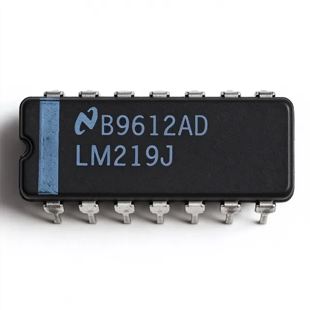
LM219J - High-Speed Dual Comparator | Texas Instruments
The Texas Instruments LM219J is a general-purpose, high-speed dual comparator with two independent comparison channels, a 5 V to 30 V supply range, and a 14-CDIP package. It is designed for applications requiring rapid logic-level decisions and compatibility with DTL, open-collector, open-emitter, RTL, and TTL interfaces. The device is supplied in a 0.300-inch, 7.62 mm ceramic dual-inline package. A comparator is an analog-to-digital decision component that compares two input voltages and produces a logic-oriented output indicating which input is higher. In the broader electronics hierarchy, the LM219J belongs to the comparator and linear IC families, alongside logic-compatible interface and signal-conditioning devices. Its two channels can be used independently for threshold detection, zero-crossing detection, pulse shaping, or basic control loops. The verified LM219J information identifies a dual general-purpose comparator, a 5 V to 30 V supply range, and DTL, open-collector, open-emitter, RTL, and TTL output compatibility. These characteristics make it useful in legacy industrial logic, control, test, and instrumentation systems where existing designs depend on high-voltage-compatible inputs and established logic interfaces. The dual-channel configuration also reduces the component count when two comparison functions are required. The LM219J family is described as a precision high-speed dual comparator fabricated on a single monolithic chip. The verified data does not provide a full electrical parameter table, propagation-delay value, input-offset specification, input-current limit, or output-current rating, so those values are not inferred here. Applications should be checked against the manufacturer datasheet before relying on timing, noise, input common-mode range, or output-drive limits. Typical uses include industrial control logic, digital threshold detection, pulse and signal monitoring, legacy computer interfaces, process-control instrumentation, and embedded systems using open-collector or TTL-compatible signaling. The 14-CDIP package favors through-hole legacy boards and repair or modernization projects rather than compact surface-mount assemblies. When upgrading a PCB, confirm pin numbering, supply polarity, input polarity, output pull-up requirements, and timing margins before substitution. For robust implementation, place the device close to the circuitry whose signals are being compared, maintain the required supply voltage, and observe the output-load requirements of the selected interface. Open-collector outputs generally need an external pull-up network, while TTL-compatible systems may use active drive. PCB layout should minimize long comparator input traces and provide adequate bypassing around the supply pins. This page combines verified distributor and cross-reference information with practical engineering guidance. It explicitly separates available facts from missing parameters so that procurement, replacement, and high-speed circuit decisions can be checked against the authoritative Texas Instruments documentation before design release.
LM239DRG4 - Quad Open-Collector Comparator | Texas Instruments
Texas Instruments LM239DRG4 is a commercial-grade quad differential comparator with four independent comparison channels, open-collector outputs, single- or dual-supply operation, and a 14-pin SOIC package. The device is intended for industrial and commercial equipment operating from -25°C to +85°C, and its open-collector outputs can pull a logic rail low when a defined sink current is available. A comparator is an analog signal-conditioning integrated circuit that evaluates a voltage at its non-inverting input against a voltage at its inverting input. The resulting digital output indicates which input is higher. Within the broader electronics hierarchy, the LM239 belongs to the comparator family, which is part of analog interface and signal-conditioning ICs used between sensors, analog measurement circuits, and digital control logic. The LM239DRG4 provides four differential comparators in one package. Its open-collector outputs are compatible with TTL, MOS, and CMOS logic according to the manufacturer information, allowing each output to operate as a wired-AND node when connected to a suitable pull-up. This architecture is useful when several signals must be monitored or when the output must directly interface with an open-collector bus. The commercial-grade temperature range supports controlled industrial environments rather than extended automotive or military temperature classes. The manufacturer describes wide single-supply or dual-supply operation, low input bias current, and low supply-current drain. Published family information identifies a typical low input bias current of 3.5 nA and a typical low supply-current drain of 0.8 mA for the legacy LM239 family. These characteristics reduce the loading imposed on high-impedance sensing circuits and make the device appropriate for battery-powered, industrial-control, and analog front-end systems where every microamp of supply demand can affect available operating time. Typical uses include overvoltage and undervoltage supervision, sensor threshold detection, window-comparator systems, motor and actuator control, and conversion of analog measurements into logic-level decisions. The four channels may also be configured for independent sensing, hysteresis, or multi-rail monitoring. Because each output is open collector, a pull-up resistor is required for normal high-state operation, and designers must verify that the selected pull-up voltage and sink current satisfy the device limits. Board design should reserve the exposed package leads and maintain adequate copper around the 14-pin SOIC footprint. Input traces should be kept short and separated from switching nodes to reduce differential noise pickup. At each comparison threshold, verify input offset, common-mode range, propagation delay, and output pull-up timing. Do not exceed the family supply or input-voltage ratings, and account for the open-collector output's finite rise time when driving capacitive loads. This product page consolidates lifecycle status, package details, functional characteristics, drop-in options, application guidance, and design notes for engineers evaluating the LM239DRG4. It also distinguishes direct replacements from legacy package variants and explains where pull-up resistors, input filtering, output loading, and thermal verification require attention.
LM239PW - Quad Open-Collector Comparator, 14-TSSOP | Texas Instruments
The Texas Instruments LM239PW is a commercial-grade quad differential comparator containing four independent voltage comparators in a 14-pin TSSOP package. It operates from a single supply or split supplies, supports input common-mode voltages that include ground, and provides open-collector outputs for wired connection to pull-up resistors. The device is specified for supply voltages up to 36 V and differential input voltages of ±38 V. A voltage comparator is an analog integrated circuit that compares two input voltages and produces a logic-level indication of their relationship. The LM239 belongs to the comparator hierarchy, within analog interface and signal-conditioning semiconductors. Unlike a general-purpose operational amplifier used for closed-loop amplification, each comparator channel primarily switches its output according to the polarity of its differential input. Its open-collector architecture makes it useful for level translation, open-drain buses, and systems that require multiple devices to share a pull-up network. The LM239PW provides four independent channels, a low typical input offset voltage of 0.37 mV, a typical input bias current of 3.5 nA, and a typical supply current of 200 µA per comparator. Its differential input range extends to ±38 V, while the common-mode input range includes ground. Open-collector outputs are compatible with TTL, MOS, and CMOS interfacing when suitable pull-up resistors are installed, and the low output saturation voltage supports reliable digital load drive. Each channel operates independently, allowing the same package to perform four unrelated sensing or thresholding functions. The wide common-mode range is particularly useful in single-supply systems where one input remains near 0 V. The low offset and bias characteristics help establish thresholds with reduced input error, while the low typical supply current per channel supports low-power monitoring systems. Split-supply operation is also possible when the total supply span and input common-mode limits are respected. Typical uses include industrial sensor interfaces, battery monitoring, overvoltage and undervoltage detection, window comparators, motor-control feedback, and general logic-level sensing. Because the outputs are open collector, pull-up resistors are required for normal high-level operation. A pull-up value should be selected from the required rise time, bus capacitance, sink-current limit, and downstream input characteristics rather than from the nominal supply voltage alone. Designers should keep input leads short, place bypass capacitance close to the supply pins, and verify that every differential and common-mode input remains inside its rated range. Output collectors must not exceed their voltage and current limits, and unused comparator channels should be brought to defined legal states. This page combines application guidance, pin-level information, design checks, and verified same-footprint alternatives to support schematic capture and board-level replacement decisions.
LM2903ATH-13 - Dual Differential Comparator, TSSOP-8 | Diodes Inc
The Diodes Incorporated LM2903ATH-13 is a dual general-purpose differential voltage comparator supplied in an 8-pin TSSOP surface-mount package, rated for supply voltages up to ±18V (36V total), with two independent high-gain comparators in a single footprint. A voltage comparator is an analog circuit element that compares two input voltages and drives its output to indicate which is higher. Within the signal-chain hierarchy, the comparator sits alongside operational amplifiers as a member of the analog IC family: where an op-amp amplifies the difference, a comparator saturates its output to a logic-compatible level, making it a bridge between the analog and digital domains. The LM2903 family - originally introduced by multiple manufacturers and now offered by Diodes Incorporated as the LM2903 series - is the industry-reference dual comparator used worldwide. Key features of the LM2903ATH-13 include two independent comparators with high open-loop gain, a wide supply range spanning single or dual supplies up to ±18V/36V, low input offset characteristics, and open-collector outputs that support wired-OR configurations and flexible logic-level translation. The TSSOP-8 package provides a compact surface-mount footprint suitable for dense boards, and the device is positioned by Diodes Incorporated for industrial, automotive, and consumer electronics applications. Technically, each comparator in the LM2903ATH-13 is a differential amplifier stage with a PNP input pair that allows input common-mode voltages extending down to the negative rail, including slightly below ground in single-supply operation. The open-collector output stage requires an external pull-up resistor, which lets designers adapt the output swing to 3.3V, 5V, or higher logic rails independently of the comparator supply. Hysteresis, when needed, is added with a small amount of positive feedback around the comparator. Typical applications include voltage threshold detection and supervision in power supplies, level shifting between analog front ends and microcontroller inputs, oscillator and timing circuits, current-sense limit detection, and signal conditioning in industrial and automotive electronic control units. A key design consideration is that the open-collector output mandates a pull-up resistor to the desired logic rail, and for slowly moving input signals a few millivolts of hysteresis should be added to prevent output chatter near the switching threshold. This page adds value beyond the manufacturer datasheet by consolidating drop-in alternative comparisons, pinout information, application guidance, and sourcing details in one place for design and procurement engineers.
LM2903EPWRQ1 - Automotive Dual Comparator | Texas Instruments
The Texas Instruments LM2903EPWRQ1 is an automotive dual differential comparator with two independent comparator channels, open-collector outputs, and operation across a 2 V to 30 V supply range. It is qualified to AEC-Q100 Grade 0 and Grade 1 and is packaged in an 8-pin TSSOP (PW) package for automotive and industrial systems. The device is intended for high-voltage signal-chain applications where a robust differential input comparator is needed to monitor two voltages and report their relationship. A comparator is an analog integrated circuit that compares an input voltage with a reference or threshold voltage and switches its output when the differential polarity changes. LM2903EPWRQ1 belongs to the differential comparator family within the broader voltage-comparison, signal-conditioning, and power-management IC hierarchy. Its differential inputs allow one signal to be evaluated against another rather than against a fixed internal reference, making it useful for threshold detection, overvoltage and undervoltage monitoring, sensor conditioning, and control systems. The dual-channel architecture provides two comparators in one package while keeping each channel independent. The open-collector output structure allows the output transistor to remain off when the output is high-impedance, which supports wired logic, pulled-up buses, and systems requiring an external pull-up resistor. The automotive qualification provides an important distinction from standard industrial comparator variants because the LM2903-Q1 family is characterized for Grade 0 and Grade 1 operating environments. Typical applications include automotive battery monitoring, 12 V and 24 V power-system supervision, sensor threshold detection, window and system monitoring, industrial control panels, and automotive actuator or interface circuits. The 30 V maximum supply rating provides useful headroom for systems with battery transients and elevated industrial rails. When designing a comparator circuit, verify the input common-mode range, output pull-up requirements, propagation delay, and the electrical limits for the intended automotive operating environment. The LM2903EPWRQ1 is supplied in an 8-pin TSSOP (PW) package, allowing compact PCB placement while supporting the pin arrangement of the LM2903-Q1 family. For new designs, confirm the selected ordering code against the manufacturer datasheet and validate the external pull-up resistor and input filtering for the specific signal environment.

LM2903M - Dual Differential Comparator | Texas Instruments
The Texas Instruments LM2903M is a dual differential comparator in an 8-pin SOIC package. It contains two independent comparator channels, operates from a single supply or split supplies, and provides open-collector output stages suitable for driving external pull-up networks. The verified distributor listing identifies the device as a standard general-purpose comparator with rail-to-rail input capability, while the linked Fairchild datasheet describes the LM2903 family as a dual differential comparator designed for operation from a 2 V to 36 V supply. The LM2903M combines two precision comparators with low input offset voltage, low supply current, and a propagation delay listed by a verified distributor source as 1.5 microseconds. A comparator is a differential amplifier with a logic output rather than a conventional analog output. It evaluates the voltage relationship between its inverting and non-inverting inputs and produces a saturated digital state when the selected input exceeds the reference. In the LM2903M, two independent channels allow one device to perform two threshold decisions, window comparisons, or complementary sensing functions. This makes the part useful as a building block within logic ICs, interface ICs, industrial control systems, and discrete analog signal-conditioning circuits. Key features include dual differential comparison, an open-collector output, single-supply operation from 2 V to 36 V, support for split-supply operation, and an 8-SOIC surface-mount package. The open-collector outputs can be wired to a common pull-up rail when multiple comparators need a shared bus, although the pull-up resistor and external logic voltage must be selected for the intended interface. The reported 1.5 microsecond response time is adequate for many industrial and control applications where the system does not require sub-microsecond decisions. The LM2903 family is designed for low-power operation independent of the supply voltage, which helps conserve energy in battery-powered and distributed equipment. Each channel has independent input and output behavior, allowing one channel to monitor a sensor while the second channel provides an alarm, window-limit, or control function. Input and output behavior should still be checked against the complete manufacturer datasheet for the exact ordering code before production use. Typical applications include battery monitoring, industrial sensor interfaces, overvoltage and undervoltage detection, temperature threshold circuits, power-supply sequencing, and general-purpose logic control. The open-collector output is especially useful when driving a relay, opto-isolator, or another device that requires a pulled-up supply domain. The SOIC-8 footprint is suitable for conventional surface-mount PCB assembly, but the exposed package dimensions and lead geometry should be checked against the mechanical drawing. For a reliable design, begin by verifying the input common-mode range, output sink current, supply-current limits, and propagation delay against the required operating conditions. Do not leave the open-collector outputs without an appropriate pull-up resistor unless the intended load provides one. Decoupling capacitors should be placed close to the supply and ground pins, and input traces should be kept short to reduce noise pickup. This product page combines verified manufacturer and distributor information with engineering guidance, comparison data, and practical design notes to support component selection and PCB implementation.

LM2903M8-13 - Dual 36V Comparator | Diodes Incorporated
The Diodes Incorporated LM2903M8-13 is a dual differential analog comparator with two independent comparison channels, a 36 V maximum supply rating, and an 8-pin MSOP package. The device supports single-supply and split-supply operation and is designed for general-purpose signal comparison with open-collector outputs compatible with TTL, CMOS, and MOS logic. An analog comparator is an integrated circuit that compares two input voltages and changes its output state according to their relationship. The LM2903 belongs to the differential-comparator hierarchy, which includes precision comparators, voltage comparators, and general-purpose analog interface ICs. Unlike an operational amplifier, a comparator is optimized for fast decision-making, open-drain or open-collector output signaling, and straightforward connection to digital logic rather than linear analog amplification. The LM2903M8-13 provides two independent comparator channels, a wide 36 V operating range, and a specified 300 ns propagation-delay class. Its low input offset voltage supports decisions when the compared signals differ only slightly. The open-collector architecture permits wired logic, pull-up resistor selection, level translation, and compatibility with multiple logic families. Operation from a single positive supply or from positive and negative split supplies makes the device suitable for both conventional and bipolar signal environments. The LM2903 series uses an open-collector output stage rather than a totem-pole output. Each output therefore requires an external pull-up resistor when used as a normal logic driver. This architecture can provide wired-AND behavior, but it can also expose unused outputs to leakage current and requires careful pull-up selection. The two channels are electrically independent, allowing one device to serve two unrelated threshold, window, sorting, or fault-detection functions. Typical uses include sensor threshold detection, battery and power-supply monitoring, window comparators, overvoltage and undervoltage protection, signal conditioning, relay or reset-control logic, and general interface between analog sensors and digital systems. In dual-rail systems, the split-supply capability supports comparison of bipolar signals. In single-supply systems, the comparator can compare a sensor output against a reference voltage while driving a pull-up-based digital output. Designers should verify input common-mode limits, output current, response time, and pull-up requirements against the intended supply conditions. Keep the comparator input and output paths away from high-current switching nodes, use short traces over a continuous ground plane, and place the pull-up resistor close to the output. Because the open-collector output cannot source current, the chosen resistor must satisfy both the required sink current and the logic-family input-current limits. This product page combines the exact LM2903M8-13 package and rating information with application guidance, engineering design notes, and verified cross-reference results. It also distinguishes confirmed same-package drop-in options from comparator parts that require a different footprint, helping PCB designers avoid substitutions that cannot be installed without redesign.