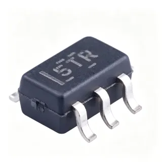
SN74LVC1T45DCKR - 420Mbps Single-Bit Dual-Supply Level Shifter | TI
MPN: SN74LVC1T45DCKR ✓ Active| Qty | Unit Price | Extended |
|---|---|---|
| 1 | $0.42 | $0.42 |
| 10 | $0.38 | $3.80 |
| 100 | $0.27 | $27.00 |
| 500 | $0.21 | $105.00 |
| 1,000 | $0.17 | $170.00 |
| 3,000 | $0.14 | $420.00 |
SN74LVC1T45DCKR Overview
A voltage-level translator (also called a level shifter) is a logic device that enables clean communication between ICs operating at different supply voltages. In modern mixed-voltage systems, a 1.8 V microcontroller may need to interface with a 3.3 V sensor or a 5 V peripheral; level translators preserve signal integrity and protect low-voltage inputs from overvoltage damage. The SN74LVC1T45 belongs to the LVC (Low-Voltage CMOS) logic family, known for high speed, low power, and broad supply compatibility, making it a fundamental building block of digital interface design.
Key features include ESD protection exceeding JESD 22 (2000-V Human-Body Model per A114-A), 5.5-V tolerant inputs, a typical propagation delay of 3.3 ns at 3.3 V, a low maximum ICC of 10 uA, and +/-24-mA output drive at 3.3 V. The Ioff feature disables outputs during power-down, preventing damaging backflow current in partial-power scenarios. The dual-supply design ensures output levels match each voltage domain, providing correct logic levels on both sides of the translation boundary.
Architecturally, the device uses CMOS logic with a DIR pin controlling data direction: DIR high routes A to B, DIR low routes B to A. The OE pin tri-states outputs for shared-bus operation. VCC isolation is designed so that if either VCC input is at GND, both ports enter the high-impedance state - critical for hot-swap and partial-power scenarios.
Typical applications include SPI and UART level shifting between microcontrollers and sensors, memory card interfaces, GPIO translation in mixed-voltage embedded systems, and automotive communication buses. Its 420-Mbps data rate suits high-speed serial links such as I2C, SPI, and UART bridges. The SC-70 package and 10-uA supply current fit portable battery-powered designs.
Design tip: decouple both VCCA and VCCB with 0.1-uF ceramic capacitors close to the pins, and drive DIR and OE to valid logic levels during power-up to avoid bus contention. This page synthesizes distributor pricing, drop-in alternatives, and practical design notes not found in the manufacturer datasheet.
Drop-in alternatives for SN74LVC1T45DCKR — same package, pin-to-pin compatible. Different-package parts requiring PCB rework are excluded.
Variants in this series
Same-series models that are drop-in compatible with SN74LVC1T45DCKR (same form factor and footprint) — differing in Channels, Function, Package, Direction Control, Input Tolerance.
Quick Comparison Tool — Select alternative parts for side-by-side comparison:
SN74LVC1T45DCKT
✅ Drop-In📋 Reference alternative (not in catalog)
SN74LVC1T45QDCKRQ1
✅ Drop-In✓ In Stock
$0.48 / Unit
View Datasheet →SN74AVC1T45DCKR
✅ Drop-In📋 Reference alternative (not in catalog)
SN74AXC1T45DCKR
✅ Drop-In📋 Reference alternative (not in catalog)
SN74LVC1T45YZPR
✅ Drop-In📋 Reference alternative (not in catalog)
SN74LVC2T45DCUR
✅ Drop-In📋 Reference alternative (not in catalog)
SN74LVC1T45DCKR Maximum Ratings & Electrical Characteristics
| Function | Single-bit dual-supply bus transceiver / voltage level translator |
| Channels | 1 channel, bidirectional |
| Data Rate | 420 Mbps |
| Direction Control | DIR pin (high = A->B, low = B->A) |
| Output Enable | OE pin, tri-states outputs when high |
| VCCA Supply Range | 1.65 V to 5.5 V |
| VCCB Supply Range | 1.65 V to 5.5 V |
| Logic Family | LVC (Low-Voltage CMOS) |
| Technology | CMOS |
| Propagation Delay (typ @ 3.3 V) | 3.3 ns |
| Quiescent Current (max) | 10 uA |
| Output Drive (at 3.3 V) | ±24 mA |
| ESD Protection | 2000 V HBM per JESD 22 A114-A |
| Input Tolerance | 5.5 V tolerant on both ports |
| VCC Isolation (Ioff) | Yes - both ports Hi-Z if either VCC at GND |
| Operating Temperature | -40C to +85C |
| Package | SC-70-6 (DCK) |
| Mounting Type | Surface Mount |
| RoHS Status | Compliant |
| Lead-Free | Yes |
SN74LVC1T45DCKR Pin Configuration
| Pin 1 | VCCA — Supply voltage for A port and DIR/OE control inputs (1.65 V to 5.5 V) |
| Pin 2 | GND — Ground (0 V reference for both supply rails) |
| Pin 3 | A — Data I/O port A - signals referenced to VCCA |
| Pin 4 | B — Data I/O port B - signals referenced to VCCB |
| Pin 5 | DIR — Direction control: HIGH routes A->B, LOW routes B->A (referenced to VCCA) |
| Pin 6 | VCCB — Supply voltage for B port (1.65 V to 5.5 V) |
Typical Applications
SN74LVC1T45DCKR is suitable for 7 applications: UART Level Shifting Between Mixed-Voltage MCUs, SPI Bus Translation for Sensors and Flash, SD Card / MMC Interface Voltage Translation, I2C Bus Translation Between 3.3 V and 5 V, GPIO Translation in Mixed-Voltage Embedded Systems, Automotive Communication Bus Bridges, Portable/Battery-Powered Device Interfacing.
UART Level Shifting Between Mixed-Voltage MCUs
The SN74LVC1T45DCKR bridges UART TX/RX lines between a 1.8 V host MCU and a 3.3 V or 5 V peripheral. Its 420 Mbps data rate easily covers standard UART rates up to 1 Mbps plus SPI peripherals; 3.3 ns propagation delay preserves timing margins in protocol stacks. Place VCCA on the MCU side and VCCB on the peripheral side; drive DIR from a GPIO to control TX/RX direction. Ioff protection prevents back-powering when either supply is off during hot-swap.
Recommended
SPI Bus Translation for Sensors and Flash
SPI peripherals (sensors, NOR flash, ADC) often operate at a different voltage than the host MCU. The SN74LVC1T45DCKR shifts MOSI, MISO, and SCLK lines individually between 1.8 V/3.3 V/5 V domains. With ±24 mA drive, it can source/sink sufficient current for capacitive loads and longer PCB traces. The OE pin tri-states MISO when the peripheral is deselected, preventing bus contention on multi-slave SPI buses shared between mixed-voltage slaves.
Recommended
SD Card / MMC Interface Voltage Translation
SD cards signal at 3.3 V while modern host SoCs may run at 1.8 V. The SN74LVC1T45DCKR shifts CMD, DAT0-DAT3, and CLK between the SoC and the card slot. The 420 Mbps rate supports UHS-I SD clock rates up to 50 MHz single data rate. Ioff isolation protects the SoC if the card is inserted/removed while the system is powered; ESD protection to 2000 V HBM guards against ESD events during card insertion.
Recommended
I2C Bus Translation Between 3.3 V and 5 V
Although the SN74LVC1T45DCKR has push-pull outputs (not open-drain), it can shift I2C SDA/SCL lines when the master always drives a single direction per line. DIR pins for SDA and SCL are tied so the master always transmits to the slave. Pull-up resistors on each voltage domain set logic high. For true bidirectional open-drain I2C, prefer a dedicated FET-based shifter like LSF0101, but for clock-stretch-free I2C at moderate speeds, the LVC1T45 works cleanly.
Recommended
GPIO Translation in Mixed-Voltage Embedded Systems
Individual GPIO signals in a mixed-voltage embedded design often need shifting. The SN74LVC1T45DCKR shifts one GPIO line per chip, with DIR controllable from the host to allow dynamic direction changes for shared lines. Examples include shifting a 1.8 V MCU interrupt line up to a 3.3 V SoC GPIO, or shifting a 5 V sensor alarm line down to a 3.3 V MCU. Multiple chips can be paralleled for multi-bit buses.
Recommended
Automotive Communication Bus Bridges
The automotive-grade variant SN74LVC1T45QDCKRQ1 (AEC-Q100 qualified) is widely used in CAN, LIN, and FlexRay transceivers that need 3.3 V to 5 V level shifting between the MCU and the bus transceiver IC. The standard SN74LVC1T45DCKR suits non-safety automotive body electronics such as infotainment, HVAC, and lighting modules where AEC-Q100 is not mandated. The SC-70-6 package fits space-constrained ECU boards.
Recommended
Portable/Battery-Powered Device Interfacing
Portable devices running from Li-ion batteries (3.0-4.2 V) often need to interface with 1.8 V sensors and 5 V chargers. The SN74LVC1T45DCKR's 10 uA max quiescent current minimizes battery drain when the device is idle, and its Ioff feature ensures zero leakage when either rail is powered down. The SC-70-6 package saves PCB area in wearables, hearables, and IoT sensor nodes where board space is at a premium.
Recommended
Recommended Products Summary
Engineering reference data for SN74LVC1T45DCKR — comparison, design guidance, and compliance information.
Selection Guide
Comparison with Alternatives
| Parameter | This Product | SN74LVC1T45DCKT | SN74LVC1T45QDCKRQ1 | SN74AVC1T45DCKR | SN74AXC1T45DCKR |
|---|---|---|---|---|---|
| Package | SC-70-6 (DCK) | SC-70-6 (DCK) - same | SC-70-6 (DCK) - same | SC-70-6 (DCK) - same | SC-70-6 (DCK) - same |
| Brand | Texas Instruments | Texas Instruments | Texas Instruments | Texas Instruments | Texas Instruments |
| Data Rate (max) | 420 Mbps | 420 Mbps | 420 Mbps | ~500 Mbps | ~500 Mbps |
| VCCA/VCCB Range | 1.65 V to 5.5 V | 1.65 V to 5.5 V | 1.65 V to 5.5 V | 1.2 V to 3.6 V | 0.9 V to 3.6 V |
| Automotive Qualified (AEC-Q100) | No | No | Yes (Grade 1, -40C to +125C) | No | No |
| Propagation Delay (typ @ 3.3 V) | 3.3 ns | 3.3 ns | 3.3 ns | ~2.0 ns | ~2.0 ns |
| Output Drive (at 3.3 V) | ±24 mA | ±24 mA | ±24 mA | ±12 mA | ±12 mA |
| Channels | 1 | 1 | 1 | 1 | 1 |
| ESD (HBM) | 2000 V | 2000 V | 2000 V | 2000 V | 2000 V |
| Unit Price (qty 1000, as of 2026-10-10) | $0.17 | $0.17 | $0.45 | $0.55 | $0.60 |
Key Differentiators
- Bidirectional bus transceiver with true 3-state output (vs SN74LVC1G3157DCKR)
- 1.65 V to 5.5 V VCC range covers all common logic domains (vs SN74AVC1T45DCKR)
- Automotive-grade variant available in same footprint (vs SN74LVC1T45QDCKRQ1)
Design Notes
Decouple both VCCA and VCCB with 0.1-uF X7R ceramic capacitors placed within 2 mm of the respective supply pins. The dual-rail design means each rail must remain above its POR threshold (~1.5 V typical) for proper translation; if either rail droops below threshold during hot-plug events, outputs may glitch. For battery-powered applications with rail collapse during sleep, the Ioff feature prevents backfeeding through the I/O pins into the collapsed rail.
Do not leave DIR or OE floating during power-up. Floating DIR may select an unintended direction and cause bus contention if both sides drive simultaneously. Floating OE may keep outputs enabled when the system intends them to be tri-stated. Tie DIR to VCCA or GND (per desired direction) via a 10 kohm resistor if not driven by a GPIO. If the controller GPIO is high-impedance at reset, use a 100 kohm pull-up on DIR.
Route A and B traces as 50-ohm controlled-impedance microstrip or stripline for data rates above 100 Mbps. Keep trace lengths matched within 5 mm if the signals are clocked pairs (e.g., SCLK with MOSI). Place the SC-70-6 device near the connector or peripheral it serves, not near the host MCU, to minimize stub lengths. Exposed thermal pad is not present on this package - no thermal relief required.
Estimated: at 420 Mbps (210 MHz fundamental), trace lengths above 25 mm may require source-series termination (22-33 ohm) to absorb reflections. The device's ±24 mA drive at 3.3 V produces fast edge rates (~1 ns) that excite stubs and vias; avoid via stubs on data traces by using blind/buried vias or by routing layers carefully. For 5 V VCCB, the output edge rates are slightly slower (~2 ns) due to the higher swing.
Compliance Information
RoHS and lead-free confirmed on TI product page. Standard part is not AEC-Q100; choose SN74LVC1T45QDCKRQ1 for AEC-Q100. Halogen-free status not explicitly listed in scraped data.