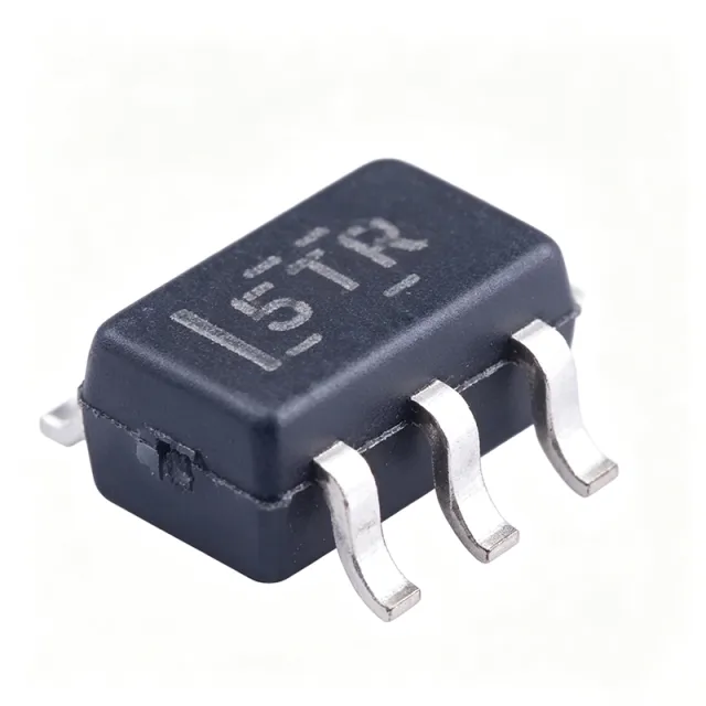
SN74LVC1T45QDCKRQ1 - Auto 1-Bit Dual-Supply Translator | TI
MPN: SN74LVC1T45QDCKRQ1 ✓ Active| Qty | Unit Price | Extended |
|---|---|---|
| 1 | $1.1 | $1.10 |
| 10 | $0.99 | $9.90 |
| 100 | $0.85 | $85.00 |
| 500 | $0.72 | $360.00 |
| 1,000 | $0.6 | $600.00 |
| 3,000 | $0.48 | $1,440.00 |
SN74LVC1T45QDCKRQ1 Overview
A voltage-level translator (also called a dual-supply bus transceiver or level shifter) is a logic IC that bridges domains operating at different supply voltages. In the broader signal-chain taxonomy, translators sit between mixed-voltage blocks such as MCUs, sensors, and transceivers, ensuring logic-level compatibility without overstressing lower-voltage silicon. They are distinct from logic gates in that they specifically isolate two supply rails while passing a digital signal between them with minimum delay.
Key features include a maximum propagation delay of 3.3 ns at 3.3V VCC, +/-24 mA output drive strength at 3.3V, low 10 uA maximum quiescent supply current, and Ioff partial-power-down support that prevents back-powering when either rail is removed. Inputs are 5.5V-tolerant regardless of VCC, and 3-state outputs place both ports in Hi-Z when a supply rail is absent. A single DIR pin selects data-flow direction per the datasheet truth table.
The device is built on TI LVC CMOS logic technology and is AEC-Q100 qualified for automotive applications, supporting an operating temperature range of -40C to +125C. It combines the speed of the 74LVC family with automotive-grade reliability, PPAP documentation, and extended-temperature screening required for body, chassis, and infotainment modules.
Typical applications include translating between 3.3V microcontrollers and 1.8V image sensors, 5V to 3.3V GPIO interfacing in body control modules, level shifting on infotainment I2C/SPI buses, and bridging UART lines between automotive domain controllers and external peripherals. The single-bit density suits one-wire-per-direction protocols such as single-wire CAN signaling or isolated UART paths.
Design consideration: keep VCCA less than or equal to VCCB where possible, ensure both supply pins are powered for proper translation, and place decoupling capacitors within 2 mm of each VCC pin to minimize switching transient coupling into translation edges.
This page synthesizes distributor pricing, pin-compatible drop-in alternatives, and practical design notes not found in the manufacturer datasheet. Pricing references are as of 2026-10-10.
Drop-in alternatives for SN74LVC1T45QDCKRQ1 — same package, pin-to-pin compatible. Different-package parts requiring PCB rework are excluded.
Variants in this series
Same-series models that are drop-in compatible with SN74LVC1T45QDCKRQ1 (same form factor and footprint) — differing in Channels, Direction Control, Function, Input Tolerance, Technology.
Quick Comparison Tool — Select alternative parts for side-by-side comparison:
SN74LVC1T45DCKR
✅ Drop-In✓ In Stock
$0.14 / Unit
View Datasheet →SN74LVC1T45QDCKRQ1 Maximum Ratings & Electrical Characteristics
| Function | Single-bit dual-supply bus transceiver with configurable voltage translation |
| Channels | 1 channel (1-bit bidirectional) |
| Direction Control | DIR pin |
| Output Type | 3-State, non-inverting |
| VCCA Range | 1.65 V to 5.5 V |
| VCCB Range | 1.65 V to 5.5 V |
| Data Rate (max) | 420 Mbps |
| Propagation Delay (max) | 3.3 ns at 3.3 V |
| Output Drive (IOH/IOL) | +/-24 mA at 3.3 V |
| Quiescent Current (ICC max) | 10 uA |
| Input Tolerance | 5.5 V tolerant regardless of VCC |
| Ioff Support | Yes (partial-power-down back-power protection) |
| Operating Temperature Range | -40 C to +125 C |
| AEC-Q100 Qualification | Qualified (Automotive Grade 1) |
| Technology | LVC CMOS |
| Package | SC-70-6 (DCK) |
| Mounting Type | Surface Mount |
| RoHS Status | Compliant |
| Lead-Free | Yes |
SN74LVC1T45QDCKRQ1 Pin Configuration
| Pin 1 | VCCA — A-port supply voltage (1.65V to 5.5V) |
| Pin 2 | GND — Ground |
| Pin 3 | A — A-port data I/O (tracks VCCA) |
| Pin 4 | B — B-port data I/O (tracks VCCB) |
| Pin 5 | DIR — Direction control: HIGH = A-to-B, LOW = B-to-A |
| Pin 6 | VCCB — B-port supply voltage (1.65V to 5.5V) |
Typical Applications
SN74LVC1T45QDCKRQ1 is suitable for 6 applications: Automotive 3.3V MCU to 1.8V Sensor Level Translation, 5V to 3.3V GPIO Interfacing in Body Control Modules, Infotainment I2C and SPI Bus Voltage Bridging, UART Bridging Between Domain Controllers, Industrial Sensor to MCU GPIO Translation, Single-Wire CAN or LIN Signaling Translation.
Automotive 3.3V MCU to 1.8V Sensor Level Translation
The SN74LVC1T45QDCKRQ1 is a strong fit for translating one GPIO or UART line between a 3.3V automotive MCU and a 1.8V image sensor or accelerometer. VCCA can be tied to the 1.8V sensor rail while VCCB ties to the 3.3V MCU rail, and the 5.5V-tolerant inputs protect the lower-voltage silicon during MCU-side overvoltage events. With 420 Mbps data rate and 3.3 ns propagation delay, the device keeps up with SPI camera interfaces and high-bandwidth GPIO toggling. AEC-Q100 Grade 1 qualification at -40C to +125C eliminates the need for downstream de-rating analysis in body and ADAS modules.
Recommended
5V to 3.3V GPIO Interfacing in Body Control Modules
The SN74LVC1T45QDCKRQ1 cleanly bridges 5V legacy GPIOs on body control modules to 3.3V MCU pins when VCCB is tied to 5V and VCCA to 3.3V. The +/-24 mA output drive at 3.3V drives long PCB traces without external buffering, and the 10 uA quiescent current keeps standby budgets intact for always-on BCM domains. Ioff partial-power-down support prevents back-powering when the 5V rail is removed during key-off, protecting the 3.3V MCU from reverse current. AEC-Q100 qualification with PPAP documentation satisfies OEM sourcing requirements.
Recommended
Infotainment I2C and SPI Bus Voltage Bridging
For infotainment clusters and head units that mix 1.8V application processors with 3.3V audio CODECs or 5V display controllers, the SN74LVC1T45QDCKRQ1 provides per-bit isolation. Placing one device per SDA/SCL or MOSI/MISO line preserves bus integrity, and the bidirectional data path allows clock or data lines to flow in either direction via the DIR pin. The 420 Mbps edge rate is well above the I2C Standard-mode 100 kHz and Fast-mode 400 kHz clocks, so the translator adds negligible timing skew. AEC-Q100 screening supports under-hood and cluster locations.
Recommended
UART Bridging Between Domain Controllers
The SN74LVC1T45QDCKRQ1 cleanly shifts UART TX/RX pairs between automotive domain controllers running at different supply voltages, such as a 5V chassis-domain MCU talking to a 3.3V zonal controller. With VCCA on the 5V side and VCCB on the 3.3V side, the bidirectional translation handles both TX and RX on two separate devices, with the DIR pin set opposite on each direction. The 3.3 ns max propagation delay introduces minimal UART turnaround overhead even at 1 Mbps baud. AEC-Q100 qualification and -40C to +125C operation cover under-hood and zonal locations.
Recommended
Industrial Sensor to MCU GPIO Translation
Although AEC-Q100 qualified, the SN74LVC1T45QDCKRQ1's wide 1.65V to 5.5V dual-rail operation makes it well-suited for industrial sensor front-ends. A 1.8V analog sensor or digital isolator output can drive the A-port while a 3.3V industrial MCU reads the B-port, with the device providing 5.5V input tolerance on the higher-voltage rail. The Ioff feature prevents back-powering on factory power-down events, and the SC-70-6 footprint keeps the BOM compact for high-density PLC and remote I/O modules. Designers repurposing automotive-grade stock for industrial use benefit from extended-temperature screening.
Recommended
Single-Wire CAN or LIN Signaling Translation
The 1-bit density of the SN74LVC1T45QDCKRQ1 matches single-wire CAN, single-wire LIN, and other one-wire-per-direction automotive protocols. VCCA and VCCB track independent rails, allowing a 12V battery-conditioned rail to drive the high-side port and a 3.3V MCU on the low-side port. The bidirectional data path with DIR control keeps the bus arbitration phase within timing spec, and the +/-24 mA drive fights back reflections on long harness stubs. AEC-Q100 Grade 1 with -40C to +125C operation tolerates underhood thermal cycles.
Recommended
Recommended Products Summary
Engineering reference data for SN74LVC1T45QDCKRQ1 — comparison, design guidance, and compliance information.
Selection Guide
Comparison with Alternatives
| Parameter | This Product | SN74LVC1T45DCKR | SN74LVC1T45DRLR |
|---|---|---|---|
| Brand | Texas Instruments | Texas Instruments | Texas Instruments |
| Package | SC-70-6 (DCK) | SC-70-6 (DCK) - same | SOT-6 (DRL) - different |
| AEC-Q100 Qualified | Yes (Grade 1) | No | No |
| VCCA Range | 1.65V to 5.5V | 1.65V to 5.5V | 1.65V to 5.5V |
| VCCB Range | 1.65V to 5.5V | 1.65V to 5.5V | 1.65V to 5.5V |
| Data Rate (max) | 420 Mbps | 420 Mbps | 420 Mbps |
| Propagation Delay (3.3V, max) | 3.3 ns | 3.3 ns | 3.3 ns |
| Output Drive at 3.3V | +/-24 mA | +/-24 mA | +/-24 mA |
| ICC (max) | 10 uA | 10 uA | 10 uA |
| Operating Temperature Range | -40C to +125C | -40C to +125C | -40C to +125C |
| PPAP Documentation | Yes | No | No |
Key Differentiators
- AEC-Q100 Grade 1 qualified single-bit translator in SC-70-6 (vs SN74LVC1T45DCKR)
- Ioff partial-power-down back-power protection (vs Discrete resistor-divider level shifters)
- Universal 1.65V to 5.5V dual-rail support (vs TXB0104 (4-bit translator))
Design Notes
Place a 0.1 uF X7R decoupling capacitor within 2 mm of each VCCA (pin 1) and VCCB (pin 6) supply pin. The SC-70-6 package has limited internal capacitance, and switching transients on either rail couple directly into translation edges if bypassing is inadequate. For noisy 5V rails, add a bulk 1 uF capacitor in parallel.
Route the A-port trace on one supply reference plane and the B-port trace on its own supply reference plane, stitching them only beneath the device. Avoid running a translated trace over a plane split, because return-path impedance causes ground bounce and translation jitter. Keep the DIR pin trace short and shielded with a ground guard on both sides if the surrounding board is dense.
Both VCCA and VCCB must be powered for the device to translate correctly. Floating either rail places the outputs in an indeterminate Hi-Z state and can latch up the device under heavy load. Verify DIR pin state at power-up; if left floating, the device defaults to B-to-A direction. Tie DIR directly to VCCA or VCCB through a 100 kohm pull-up or pull-down resistor to define a known startup direction.
Compliance Information
AEC-Q100 Grade 1 qualified automotive part with PPAP documentation, RoHS and REACH compliant per TI product page.







