Platinen & Module
Unterkategorien
Produkte (217)

ROG Zephyrus G16 (2026) GU606 Gaming Laptop | ASUS Republic of Gamers
The ASUS Republic of Gamers (ROG) Zephyrus G16 (2026) GU606 is a high-performance 16-inch gaming laptop integrating an NVIDIA GeForce RTX 5090 mobile GPU with an Intel Core Ultra (Series 2) processor on a 2.5K OLED display panel. It is positioned as ASUS's flagship ultraportable gaming platform, with a chassis designed around the NVIDIA Blackwell laptop architecture and Intel's Lunar/Meteor Lake successor CPUs. A gaming laptop is a portable computing platform engineered specifically for real-time 3D rendering, high-refresh-rate displays, and sustained thermal loads that exceed typical ultrabook designs. Within ASUS's product hierarchy, the ROG (Republic of Gamers) line sits above consumer VivoBook and ZenBook lines and alongside the TUF Gaming line, targeting enthusiast and competitive gaming segments. The Zephyrus sub-brand within ROG focuses on thin-and-light premium gaming, while Strix targets maximum performance, Flow targets convertible/tablet form factors, and Ally targets handheld PC gaming. Key features of the GU606 (2026) include the RTX 5090 mobile GPU with the latest generation of NVIDIA CUDA, RT, and Tensor cores, a 2.5K-resolution OLED panel (commonly 2560x1600) with high refresh rate support, and ASUS's ROG Intelligent Cooling thermal system using liquid-metal compound and arc-flow fans. Memory configurations scale to high-capacity DDR5 and PCIe Gen4/Gen5 NVMe storage. The chassis is CNC-machined aluminum with the ROG AniMe Matrix LED lid on certain SKUs. Technically, the platform supports NVIDIA Advanced Optimus and MUX switch for direct GPU output to the internal display, reducing latency for competitive gaming. The OLED panel's per-pixel dimming enables a 1,000,000:1 contrast ratio and DisplayHDR True Black certification, distinguishing it from the IPS panels used in earlier Zephyrus generations. Wi-Fi 7 connectivity and Thunderbolt 4/USB4 expand docking options. Typical applications include AAA gaming at high frame rates, esports with low-latency display output, content creation (video editing, 3D rendering) leveraging the GPU's Tensor cores, and game streaming through software like OBS Studio. The OLED display also makes the platform suitable for HDR movie playback and color-accurate creative work. When selecting this SKU, evaluate GPU power-budget tier (RTX 5090 vs RTX 5080/5070 variants), RAM soldered-vs-upgradable, and whether the AniMe Matrix lid is desired. Cooling acoustics and chassis thickness vary by GPU tier — higher-TGP variants produce more fan noise under sustained load.
SATAPMH141-SE - 1-to-4 SATA Port Multiplier 3Gbps | IOI
The IOI SATAPMH141-SE is a 1-to-4 SATA port multiplier module based on the Marvell 88SM8040 controller, allowing a single SATA host port to communicate with up to 4 SATA device ports plus one SEMB (Port Multiplier Management) port, with 3Gbps serial link capability on all SATA links. A SATA port multiplier is a storage interconnect device that expands a single host SATA controller port into multiple device-facing SATA ports. In the storage hierarchy it sits between the host SATA controller (AHCI or FIS-based switching) and SATA disk drives or SSDs, aggregating traffic so that one physical host link serves several devices. This reduces host controller count in multi-drive systems such as NAS enclosures, RAID chassis, and storage appliances. Key features of the SATAPMH141 include its unique data aggregation capability, which lets the module exploit the full 3Gbps host link bandwidth when paired with FIS-based switching host controllers, and its support for up to four device ports simultaneously. The -SE suffix denotes a specific configuration variant within the SATAPMH141 product family from IOI (I/O Interconnect), which specializes in SATA and SAS connectivity hardware. Architecturally, the Marvell 88SM8040 handles command frame (FIS) switching between host and devices, frame arbitration, and port state management, presenting each drive as a distinct SATA device to the host. Performance is bounded by the shared 3Gbps host link, so sustained aggregate throughput peaks at roughly 300 MB/s across all drives combined. Typical applications include multi-bay external drive enclosures, NAS backplane designs, low-cost RAID expansion, and industrial storage subsystems where host SATA ports are scarce. The module form factor allows direct integration onto carrier boards. A key design consideration: allocate bandwidth across attached drives carefully, since the host link is shared - concurrent heavy access to four drives will divide the 3Gbps link. Verify that your host controller supports FIS-based switching for best aggregation; command-based switching hosts offer lower effective bandwidth. This page synthesizes manufacturer product data, drop-in alternatives, application guidance, and design notes not found on the standard manufacturer product listing.
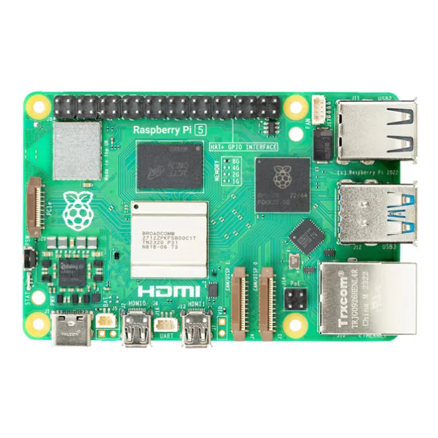
SC1111 - Raspberry Pi 5 4GB SBC 2.4GHz Cortex-A76 | Raspberry Pi | Desktop & Industrial
The Raspberry Pi 5 (SC1111, 4GB) is a single-board computer built upon a 64-bit quad-core 2.4 GHz Arm Cortex-A76 processor with 4GB of RAM on the full-size Raspberry Pi form factor. Per the official product data, its CPU delivers a two to three times increase in performance compared to Raspberry Pi 4, and it is the first full-size Raspberry Pi computer developed with silicon designed in-house by Raspberry Pi. Data verified as of 2026-09-13. A single-board computer (SBC) is a complete computer system integrated onto one printed circuit board, combining processor, memory, I/O interfaces, and power management without the need for a separate motherboard. Within the category hierarchy, the SBC sits between embedded compute modules and full desktop PCs, making it the standard platform for prototyping, education, and industrial edge deployments. Raspberry Pi popularized this form factor, and the Raspberry Pi 5 is its current full-size generation. Key characteristics of the SC1111 include the in-house-developed application processor running at 2.4 GHz, the substantial generational CPU performance uplift over Raspberry Pi 4, and the retained compatibility ethos of the full-size Raspberry Pi layout, which preserves the ecosystem of HAT add-on boards, cases, cameras, and displays that the community and industry have built over multiple generations. From a technical standpoint, the move to custom in-house silicon marks a strategic shift for Raspberry Pi: controlling the SoC design allows tighter integration between CPU, peripherals, and power architecture, which historically translates into better performance per watt and more predictable long-term supply. The quad-core Cortex-A76 core is an Armv8.2-A 64-bit architecture widely deployed in mainstream Android and Chromebook devices, so software toolchains, compilers, and Linux distributions are mature for this target. Typical applications include desktop-class computing and productivity use, industrial automation and edge data logging, robotics control, digital signage, and networked media or AI inference at the edge where local processing avoids cloud dependency. The 4GB memory configuration suits workloads such as lightweight servers, automation controllers, and multi-service IoT gateways. A practical design consideration: verify your power supply meets the board requirements from the official Raspberry Pi documentation before deployment, and confirm HAT mechanical and electrical compatibility when migrating from Raspberry Pi 4, since peripheral interfaces have been updated on this generation. What this page adds beyond the datasheet: a consolidated SC1111 price comparison across authorized distributors (Octopart lists 3 distributors, with PCBX quoting $68.56056 as of 2026-09-13), drop-in and functional alternative analysis within and beyond the Raspberry Pi 5 series, and practical deployment notes for desktop, industrial, and robotics use of this Arm Cortex-A76 single-board computer.
SC1112 - Raspberry Pi 5 8GB SBC, 2.4GHz Cortex-A76 | Raspberry Pi | Edge AI & IoT
The Raspberry Pi 5 (SC1112, 8GB) is a single-board computer built around a 64-bit quad-core 2.4GHz Arm Cortex-A76 processor (Broadcom BCM2712) with 8GB of LPDDR4X SDRAM, delivering two to three times the CPU performance of Raspberry Pi 4 on the standard full-size Raspberry Pi form factor. Data verified as of 2026-09-13. A single-board computer (SBC) is a complete computer fabricated on a single printed circuit board, integrating processor, memory, storage I/O, and connectivity. The Raspberry Pi 5 sits at the top of the Raspberry Pi single-board computer family, which belongs to the broader category of embedded computers, and was developed by Raspberry Pi with its own in-house silicon (BCM2712), a first for the company. Key features of the SC1112 include the 2.4GHz Cortex-A76 quad-core CPU, an 8GB memory configuration (a mid-tier option in the Raspberry Pi 5 series), and the standard 40-pin GPIO header for Hardware Attached on Top (HAT) expansion. Per the official Raspberry Pi product brief, the Pi 5 architecture enables two to three times the speed of other generations. From a technical standpoint, the BCM2712 integrates four Arm Cortex-A76 cores, a high-performance Armv8.2-A-class microarchitecture, with a modern GPU subsystem and I/O fabric. The 8GB LPDDR4X memory pool is the defining differentiator of SC1112 versus the 2GB, 4GB, and 8GB variants, allowing larger working sets for in-memory data processing, multi-container edge deployments, and desktop-class multitasking. Typical applications include edge AI inference and data logging, industrial IoT gateways, robotics control, and desktop-class computing where a compact, low-power Linux computer is required. The 40-pin GPIO header and broad OS support (Raspberry Pi OS, Ubuntu, and others) make it a strong fit for automation and prototyping. A practical design consideration: the higher CPU and memory throughput of Raspberry Pi 5 increases sustained power draw versus Raspberry Pi 4; plan the 5V USB-C power supply and thermal management (heatsink or fan) according to the official Raspberry Pi documentation. Beyond the datasheet, this page provides an SC1112 vs SC1111 (4GB) vs cross-brand SBC comparison, terminal-level 40-pin GPIO wiring reference, design notes, and sourcing information with prices refreshed as of 2026-09-13.
SC1113 - Raspberry Pi 5 16GB SBC, 2.4GHz Cortex-A76 | Raspberry Pi | Edge AI
The Raspberry Pi 5 (SC1113, 16GB) is a single-board computer built around a Broadcom BCM2712 SoC with a 4-core 64-bit Arm Cortex-A76 CPU running at 2.4GHz, 16GB of LPDDR4X SDRAM, and a VideoCore VII GPU, on the standard 85.6 x 56.5mm Raspberry Pi form factor. Data verified as of 2026-09-13. A single-board computer (SBC) is a complete computer system fabricated on a single printed circuit board, integrating the processor, memory, power management, storage interface, and I/O connectors on one board. SBCs sit within the broader category of embedded computers and are widely used where a full PC is unnecessary but general-purpose computing, networking, and expandable I/O are still required. Key features of the SC1113 include the largest memory option in the Raspberry Pi 5 family (16GB LPDDR4X, shared as system and GPU memory), dual 4Kp60-capable HDMI outputs, USB 3.0 and USB 2.0 ports, a PCI Express interface for NVMe storage, dual-band Wi-Fi and Bluetooth, Gigabit Ethernet, and the 40-pin GPIO header that supports HAT expansion boards. The updated power management IC integrates a real-time clock and charging circuitry, and heat dissipation was improved over the Raspberry Pi 4 generation. On the technical side, the VideoCore VII GPU supports OpenGL ES 3.1 and Vulkan 1.2, enabling modern graphics stacks and compute workloads. The faster BCM2712, camera/display interfaces (MIPI), and USB improvements over the predecessor make the Raspberry Pi 5 the most capable board in the Raspberry Pi lineup. The PCIe 2.0 x1 lane allows high-speed NVMe SSDs for storage-heavy applications, while the 40-pin header retains compatibility with the broad HAT ecosystem. Typical applications for the 16GB variant include edge AI inference where large models benefit from higher RAM, desktop computing with many open applications, lightweight virtualization or container hosting, media servers, and industrial gateways aggregating multiple data streams. A practical design consideration: use the recommended 5V/5A USB-C power supply; under sustained multi-core load the board draws significant power, and undervoltage from weak supplies is the most common cause of instability and SD card filesystem corruption. This page adds value beyond the datasheet by cross-referencing SC1113 against other Raspberry Pi 5 memory variants (SC1111 8GB, SC1112 4GB), detailing the 40-pin GPIO terminal map, and giving selection guidance for choosing between RAM tiers based on workload and budget.
SI5365/66-EVB - Clock Multiplier/Jitter Attenuator Eval Kit | Skyworks
The Skyworks Solutions SI5365/66-EVB is an evaluation board for the Si5365 and Si5366 any-frequency precision clock multiplier and jitter attenuator devices, supplied with the board, a cable, a CD containing documentation, and EVB configuration software at an MSRP of $350.00 (as of 2026-10-10). Note that this evaluation kit, along with the Si5365/66 devices it supports, is not recommended for new designs (NRND). An evaluation board (EVB) is a printed circuit assembly that mounts a target integrated circuit together with the supporting power, clocking, filtering, and connector circuitry required to exercise the device in a laboratory environment. EVBs sit within the broader hierarchy of development boards, kits, and prototyping hardware, and they bridge the gap between a datasheet and a production PCB by letting engineers verify jitter, phase noise, lock behavior, and output signal integrity before committing to a layout. The SI5365/66-EVB supports simplified evaluation of the Si5366 jitter-attenuating clock and the Si5356 low-jitter clock multiplier. The Si5365 family provides any-frequency synthesis with user-programmable output frequencies, while the Si5366 adds jitter attenuation for cleaning up noisy reference clocks in synchronized systems such as SONET/SDH, OTN, and synchronous Ethernet equipment. The kit ships with the evaluation board, a USB/interface cable, a CD with documentation and the EVB control software, allowing register-level configuration of loop bandwidths, output dividers, and frequency plans from a PC. This software-driven control flow is the fastest way to characterize the device's phase-noise performance with external test equipment. Typical evaluation scenarios include Telecom line-card clocking, network synchronization (SyncE/PTP) reference generation, and lab prototyping of low-jitter clock trees for high-speed data converters and FPGA/ASIC reference inputs. Design consideration: because the Si5365/66 platform is not recommended for new designs, use this board only to evaluate or support existing designs, and plan a migration path to Skyworks' current-generation timing parts. This page synthesizes distributor pricing, lifecycle status, and kit contents from manufacturer and distributor data not always surfaced in a single datasheet.
SI5367/68-EVB - Si5367/Si5368 Clock Evaluation Board | Skyworks
The Skyworks Solutions SI5367/68-EVB is an evaluation board for the Si5367 low-jitter precision clock multiplier and the Si5368 jitter-attenuating clock, supplied with a board, cable, and CD, and designed for simplified evaluation of any-frequency precision clock multiplication and jitter attenuation. A clock generator evaluation board is a hardware development tool that lets engineers characterize the timing performance of a clock IC before committing to a PCB design. Within the timing hierarchy, it sits under Clock & Timing development tools, which belong to the broader family of semiconductor evaluation kits used alongside clock generators, jitter attenuators, and precision clock multipliers. Evaluation boards expose the IC's inputs, outputs, and configuration interfaces on a ready-made PCB, saving weeks of design effort during device selection and prototyping. The key feature of this kit is dual-device support: it evaluates both the Si5368 jitter attenuating clock and the Si5367 low-jitter clock multiplier on one platform. The Si5367 accepts four clock inputs ranging from 10 MHz to 707 MHz and generates five frequency-multiplied clock outputs ranging from 2 kHz to 945 MHz, with select frequencies to 1.4 GHz, per the Skyworks Si5367 datasheet. This makes it possible to measure phase noise, jitter, and output format behavior across an extremely wide frequency range without soldering or layout work. Technically, the Si5367 family uses a digitally controlled oscillator (DCO)-based architecture with uP-programmable loop parameters, allowing any-frequency synthesis from a simple configuration file loaded over the onboard interface. The evaluation board provides the necessary power regulation, input clock conditioning, and output SMA-style connections so that laboratory instruments such as phase-noise analyzers and oscilloscopes can connect directly. Supplied contents per the distributor datasheet listing are the board, a cable, and a CD containing configuration and documentation. Typical applications include line-card and optical module clock design for SONET/SDH and Ethernet systems, verification of jitter cleanup performance for noisy reference clocks, and lab characterization of frequency plans for FPGA, ASIC, and networking PHY designs requiring sub-picosecond level clocking. A key design consideration: Skyworks marks this evaluation kit as not recommended for new designs (NRND), so use it for evaluating existing designs or for prototyping with the Si5367/Si5368 devices while considering newer Skyworks Si5xx timing platforms for new product development. This page synthesizes distributor pricing, lifecycle status, datasheet links, and practical evaluation guidance not consolidated in the manufacturer datasheet.
SOMOMAPL138-10-1603QHIR - OMAP-L138 SOM 375MHz DSP 128MB | Beacon EmbeddedWorks
The Beacon EmbeddedWorks SOMOMAPL138-10-1603QHIR is an OMAP-L138 System-on-Module (SOM) integrating the Texas Instruments OMAP-L138 dual-core SoC, which combines a 375 MHz ARM926EJ-S RISC host processor with a 375 MHz TMS320C6748 floating-point VLIW DSP. The module ships with 128 MB of DDR2 SDRAM and 16 MB of SPI flash, providing an immediately deployable compute platform for industrial temperature (-40C to +85C) embedded applications. A System-on-Module (SOM) is a small PCB that integrates a microprocessor, memory, power management, and boot peripherals into a single assembly, exposing a standardized high-speed expansion connector to a customer carrier board. By abstracting the high-risk CPU/memory/power design into a pre-validated module, an SOM accelerates time-to-market, reduces EMC and thermal debugging, and allows the OEM to focus on the application-specific I/O. Within the broader hierarchy, this product sits as: SOM -> Computer-on-Module -> Embedded Module -> Board-level Product -> Semiconductor-based subsystem. Key features of the SOMOMAPL138-10-1603QHIR include the heterogeneous ARM+DSP architecture, which enables deterministic DSP code offload for low-latency signal processing while the ARM core runs Linux or a real-time OS for control, networking, and HMI. The module exposes the OMAP-L138's peripheral set (EMAC, USB, McASP, SPI, I2C, UART, EMIFA, SATA) via a 200-pin high-speed board-to-board connector. Integrated LDO and switching regulators on the module accept a single 5V input, simplifying carrier-board power design. Typical applications for this SOM include industrial audio and biometric signal processing, machine-vision front ends, portable medical instrumentation, sensor-fusion data loggers, and industrial control gateways. The OMAP-L138's C6748 DSP delivers up to 300 MFLOPS, sufficient for FFT-based vibration analysis, motor-control loops, predictive maintenance algorithms, and multi-channel audio codec handling. The ARM9 host handles Ethernet/USB connectivity, file system, and user interface tasks. When integrating this module, route high-speed USB, EMAC, and DDR traces on the carrier with controlled impedance and length matching per the OMAP-L138 hardware design guide. Provide bulk decoupling at the 5V input and adhere to the keep-out zones specified in the mechanical drawing. This page synthesizes distributor pricing, drop-in alternatives, and engineering design notes that are not available in the manufacturer's brief datasheet summary.
SST-PFB3-PCI - Profibus DP PCI Interface Card | Molex Woodhead
The Molex Woodhead SST-PFB3-PCI is a third-generation PROFIBUS DP interface card that connects a PCI-bus host computer to PROFIBUS DP-V0, DP-V1, and FDL networks, delivering deterministic high-speed communication for industrial automation systems. It supports DP-Master Class 1 and Class 2 operation, DP-Slave mode, and FDL (Layer 2) messaging, and integrates an onboard CPU that offloads the PROFIBUS protocol stack from the host CPU. The card is a standard half-height PCI card (175 x 107 mm) operating in industrial temperature environments. A PROFIBUS interface card is a dedicated hardware adapter that lets a Windows or Linux industrial PC, PLC backplane, or SCADA server exchange real-time I/O data with field devices such as remote I/O blocks, variable-frequency drives, encoders, and valve manifolds over the PROFIBUS DP (Decentralized Periphery) fieldbus. PROFIBUS DP is an IEC 61158 / EN 50170 standard fieldbus widely deployed in factory automation, process control, and motion-control applications. Within an automation hierarchy, a PROFIBUS card sits between the controller layer (PLC/industrial PC) and the device/field layer, providing deterministic cyclic I/O and acyclic parameterization channels. The SST-PFB3-PCI acts as the controller-side endpoint for those networks. Key features include support for PROFIBUS DP-V0, DP-V1, and FDL messaging, Master Class 1 and Class 2 capability, automatic 5 V / 3.3 V PCI signaling-level detection for universal motherboard compatibility, and downloadable application firmware modules that enable product-level behavior. An onboard processor manages the protocol stack, freeing the host CPU for application logic. The card is backward-compatible where possible with the legacy SST 5136-PFB-PCI, although it is not a drop-in replacement for that older board. The SST-PFB3-PCI is most often deployed in industrial PCs that act as PROFIBUS masters communicating with distributed I/O such as Siemens ET200, ABB drives, or third-party valve terminals. It is used in SCADA and HMI hosts that need to poll remote I/O racks, in PLC programming stations that must download project data to PROFIBUS-coupled controllers, and in test rigs and laboratory automation racks that exchange deterministic I/O with PROFIBUS-coupled instrumentation. The onboard CPU offload makes it suitable where deterministic latency is required regardless of host load. When integrating the SST-PFB3-PCI, verify that the host motherboard is fully PCI 2.2 (or later) compliant, because the optional 3.3 V supply in PCI 2.1 may not power the card on some legacy boards. Use a shielded PROFIBUS DP cable with a 9-pin D-sub connector, and terminate the segment with the standard PROFIBUS terminator at both ends. Configure the baud rate (9.6 kbps to 12 Mbps) to match the slowest device on the segment, and update the card firmware via the SST configuration tool before commissioning.
ST16000NM001G - Exos X16 16TB SATA 6Gb/s Enterprise HDD | Seagate
The Seagate ST16000NM001G is a 16 TB enterprise-class 3.5-inch hard disk drive from the Exos X16 family, spinning at 7,200 RPM over a SATA 6 Gb/s interface with a 256 MB cache buffer and 512e/4Kn sector format. It is built for hyperscale and rack-dense data-center deployments where maximum capacity per U is the primary buying criterion. The Exos X16 line ships in both SATA and SAS variants, and the ST16000NM001G specifically uses the SATA 6 Gb/s dual-port-incompatible interface used by mainstream server and JBOD backplanes. A hard disk drive (HDD) is a non-volatile storage device that records data on rotating magnetic platters accessed by a moving actuator arm; it sits in the storage hierarchy below NAND SSDs on a cost-per-terabyte basis while exceeding them on raw sequential throughput at high queue depths. Enterprise HDDs like the Exos X16 are purpose-engineered for 24×7 operation, with sealed helium-filled assemblies, vibration compensation for neighboring drives, and workload ratings far above consumer or NAS drives. ST16000NM001G operates within the LFF (Large Form Factor, 3.5-inch) standard and is the highest-capacity tier of the X16 generation. Key features include 16 TB raw capacity (formatted), 7,200 RPM spindle speed, SATA 6 Gb/s (SATA III) interface, 256 MB DRAM cache, 512e/4Kn Fast Format emulation, sustained 261 MB/s transfer rate (read) per the manufacturer datasheet, and an MTBF rated at 2.5 million hours. The drive ships in helium-filled 3.5-inch form factor weighing approximately 670 g with a 5-year limited warranty. Random read latency is sub-millisecond, while the workload rate limit is rated for 550 TB per year transferred, far exceeding typical NAS drives at 180-300 TB/yr. The drive uses conventional magnetic recording (CMR) on PMR platters, not shingled magnetic recording (SMR), making it suitable for RAID rebuilds and random-write workloads where SMR drives suffer throughput collapse. The helium fill enables 9 platters at 16 TB total without the air-turbulence losses that limit 8-platter air-filled drives. Power-on hours are rated for 24×7 continuous operation, and the dual-plane motor balancer reduces acoustic and rotational vibration in dense chassis. Typical applications include hyperscale object stores (Ceph, S3-compatible), enterprise backup targets, cold-storage archives, video surveillance NVR arrays, and large-capacity RAID-6 / RAID-Z2 pools. The 16 TB capacity point typically yields the lowest $/TB in the Exos lineup. For random-write-heavy virtualization workloads, a hybrid of ST16000NM001G plus SSDs for caching/tiering is the standard pattern. Design considerations: validate the host backplane is SATA III compatible (not SAS-only), confirm the chassis supports the 26.11 mm z-height and 670 g weight, and budget for the 8-10 W typical operating power when sizing cooling. The 512e sector format requires modern OS support (Windows 8+, Linux kernel 2.6.33+) and may need alignment tuning for legacy partitions. RAID rebuild time at 16 TB will exceed 12 hours on a busy array — plan for the workload impact. This page synthesizes distributor pricing, real-world reliability data points, drop-in alternatives from competing 16 TB enterprise SATA lines, and deployment notes that go beyond the manufacturer datasheet. The information gain: a side-by-side of CMR vs SMR behavior at this capacity, which the datasheet does not make obvious.
TG765S-UT - 7-inch TouchWin HMI Touch Screen | XINJE
The XINJE TG765S-UT is a 7-inch industrial human-machine interface (HMI) touch screen from the TouchWin TG765S series, featuring an 800 x 480 resolution display, USB-B download port, USB-A flash disk port, and RS-232/422/485 serial communication support, housed in an ultra-thin panel-mount enclosure powered from a DC 24V supply. According to the XINJE TouchWin TG765 series user manual, the TG765S-UT is the universal (UT) variant of the 7-inch TG765S family, alongside the MT, ET (Ethernet) and XT variants. An HMI (human-machine interface) is an industrial operator terminal that provides a graphical touchscreen window into automation equipment. In the control-system hierarchy, the HMI sits above the PLC (programmable logic controller) and servo drives, letting operators set parameters, trigger recipes, view alarms, and monitor process variables without a PC. HMIs are a core component of SCADA, machine control, and factory automation systems. Key features of the TG765S-UT include a 7-inch color TFT touchscreen with 800 x 480 pixel resolution, low power consumption with fast operation speed and stable performance per the manufacturer product listing, a DC 24V input supply (nominal range DC 22V to DC 26V, approximately 200 mA consumption for the TG765 family), and serial ports supporting RS-232, RS-422, and RS-485 protocols for direct connection to XINJE XD/XL series PLCs and third-party controllers. The UT suffix denotes the USB port configuration: a USB-B port for project download and a USB-A port for flash disk (USB memory) project transfer. The TG765S-UT is programmed with XINJE TouchWin Editor software, which supports the full TG765 series including TG765-MT, TG765-UT, TG765-ET, TG765-XT-C, TG765S-MT, TG765S-XT and TG765S-UT. Projects developed for the standard TG765-UT typically port to the TG765S-UT with minimal changes, since both share the 7-inch 800 x 480 display format. Typical applications include industrial machinery operator panels, packaging and textile machine control, water treatment and pump station monitoring, and small OEM automation cells where a compact, low-cost touch terminal replaces physical buttons and indicator lamps. Its ultra-thin panel-mount format fits standard 7-inch cutouts in control cabinet doors. A key design consideration: verify the supply rail tolerance (DC 22V to DC 26V) and isolate the 24V supply from inductive loads, and confirm the required serial protocol (232/422/485) versus Ethernet before selecting between the UT and ET variants, as the ET model adds an Ethernet port for networked SCADA access. This page synthesizes distributor availability, same-family drop-in alternatives, and practical integration notes not consolidated in the manufacturer datasheet, providing engineers a single citable reference for the TG765S-UT.
TG765S-XT - 7in 800x480 TouchWin HMI | XINJE
The XINJE TG765S-XT is a 7-inch industrial TouchWin human-machine interface with an 800×480 TFT LCD, a 4-wire resistive touchscreen, and a DC22–26 V power input. The panel supports 16.77 million true colors, LED backlighting, 128 MB memory, and 64 MB storage according to the verified product listings. Its normal-type enclosure is identified as the TG765S-XT configuration, while the XT interface designation denotes a USB-B port with clock. Verified listings also identify an RS-232 PLC communication port and a USB-B download/upload port, making the unit suitable for compact machine-control panels where a dedicated operator display is required. A human-machine interface, or HMI, is an industrial operator panel that translates machine and process status into visual screens, buttons, indicators, and control actions. In the automation hierarchy, an HMI connects a PLC or other controller to an operator, combining display electronics, touch input, communications, and embedded control software. The TG765S-XT belongs to XINJE’s TG765S TouchWin family, intended for compact equipment interfaces, machine diagnostics, parameter entry, and process visualization. The verified data identifies an ARM9 processor operating at 400 MHz, 128 MB RAM, and 64 MB ROM or storage. The display uses TFT technology with LED backlighting, while the 4-wire resistive touch panel provides a practical interface for industrial environments. The specified operating range is 0°C to 50°C, and the front panel is rated IP65. The listed power requirement is DC22–26 V with 200 mA consumption, so system designers should provide regulated 24 VDC power with appropriate margin. Typical installations place the TG765S-XT beside a PLC, variable-frequency drive, temperature controller, or other automation equipment. The HMI can display operating parameters and receive operator commands through its documented communication and USB interfaces. Compared with a larger touchscreen, the 7-inch format limits panel space while retaining 800×480 resolution and 16.77 million-color visualization. For installation, verify the panel cutout, front-panel sealing, and cable routing against the manufacturer’s mechanical documentation. Do not substitute RS-232 or USB-B wiring assumptions for the exact terminal assignments in the TG765S-XT manual. The verified search results include a PDF product document and a TG765 series user manual, which should be consulted for complete mechanical drawings, wiring, software configuration, and environmental limits. This page consolidates the verified TG765S-XT specifications, source links, application context, and purchasing constraints. It does not infer missing mechanical dimensions, lifecycle commitments, or unverified alternative equivalence; those values should be confirmed with XINJE or the supplying distributor before production release.
TJA1145A-EVB - TJA1145A High-Speed CAN Transceiver Evaluation Board | NXP
The NXP Semiconductors TJA1145A-EVB is an evaluation board for the TJA1145A, a stand-alone high-speed CAN transceiver with partial networking, fail-safe features, and advanced power management, designed for automotive and industrial CAN FD networks. The board implements the TJA1145A in a production-representative schematic with onboard CAN bus termination, SPI control interface, and Arduino Uno pinout compatibility so that it can be paired with any microcontroller board providing USB-to-SPI bridging. It is also drop-in compatible with the S32K1xx evaluation board series from NXP. A CAN transceiver is the physical-layer interface between a microcontroller's CAN protocol controller and the differential CAN bus. The TJA1145A supports classic CAN and CAN FD at data rates up to 5 Mbit/s, with selective wake-up and partial networking that lets an ECU remain quiescent on the bus until addressed, an important feature for automotive networks that must stay electrically present but draw micro-amps when idle. The transceiver is AEC-Q100 qualified, operates from a 4.5 V to 28 V supply (with 40 V load-dump tolerance), and integrates bus fault diagnostics. Key features exposed on the EVB include the high-speed CAN bus drivers, integrated 5 V LDO output for the host MCU, SPI register access for partial-networking configuration, hardware reset and wake inputs, and pin-selectable CAN HS or CAN FD modes. The board exposes the CANH/CANL differential pair on screw terminals for direct connection to a real bus or a CAN analyzer. Two user LEDs reflect TX/RX activity and power status. Typical applications include rapid prototyping of automotive body controllers, gateway ECUs, partial-networking nodes, industrial CAN-FD sensor backbones, and bench characterization of TJA1145A sleep current, wake-up timing, and bus fault behavior. The EVB lets engineers evaluate algorithm, register map, and bus behavior before committing to a PCB spin. Design consideration: when measuring sleep or standby current on the EVB, isolate the USB-to-SPI bridge supply so its quiescent draw does not mask the TJA1145A's microamp-level sleep signature. The board's Arduino Uno headers supply the host MCU; check jumper settings so the MCU is not back-powered through the SPI lines. This page synthesizes distributor pricing, drop-in alternatives, and practical design notes not found in the manufacturer datasheet.
TMC6460-EVKIT - Smart FOC Servo Driver Eval Kit | ADI Trinamic
The Analog Devices (formerly Trinamic) TMC6460-EVKIT is a complete evaluation kit for the TMC6460 fully-integrated servo drive IC, packaged with the TMC6460-EVAL main board plus the Eselsbruecke and Landungsbruecke interface boards as part of the ADI Trinamic TMCL ecosystem. The TMC6460 integrates field-oriented control (FOC) controller, gate driver stage, current sensing, and a feedback engine on a single chip, providing a compact servo solution for brushless DC and PMSM motors up to several hundred watts. What is a smart FOC servo driver? Field-Oriented Control (FOC) is a motor-control technique that decouples torque and flux by transforming stator currents into a rotating reference frame, enabling sinusoidal torque generation, low torque ripple, and high dynamic response. A smart FOC servo driver combines the FOC algorithm, MOSFET/IGBT gate drivers, current-sense amplifiers, and encoder/hall feedback hardware in a single IC, eliminating the need for a separate microcontroller and external power stage. This integration reduces BOM count, PCB area, and firmware complexity for motion-control designs. Key features of the TMC6460-EVKIT include support for three-phase BLDC and PMSM motors, integrated FOC algorithm with programmable PI controllers, integrated gate drivers for external N-channel MOSFETs, on-chip current sensing amplifiers, Hall sensor and encoder feedback inputs, and TMCL (Trinamic Motion Control Language) scripting capability. Communication interfaces include UART, SPI, and CAN for host MCU integration. The kit enables rapid prototyping of servo applications without requiring custom firmware development for the motor-control core. The TMC6460-EVKIT targets industrial automation, robotics, CNC machinery, and precision positioning systems where deterministic servo performance, low acoustic noise, and high torque-bandwidth are required. Combined with the TMCL firmware stack and ADI Trinamic tools, engineers can parameterise motors, tune PID loops, and visualise motion profiles within minutes. The Eselsbruecke and Landungsbruecke boards provide isolated USB-host connectivity and standard TMCL I/O headers for sensor and actuator expansion. When designing with this evaluation kit, ensure the host PC provides a stable 12-24 V supply to the EVAL board's power input and observe ESD precautions when connecting to powered motors. The kit ships with TMCL-IDE software for parameter tuning, real-time charting, and firmware updates across the entire ADI Trinamic ecosystem.
TP04P-22XA1R - 4-Line Text Panel HMI + PLC 24VDC | Delta Electronics
The Delta Electronics TP04P-22XA1R is a TP Series Text Panel HMI with an integrated PLC, operating on 24 VDC, featuring a 4-line monochrome STN-LCD display (approximately 101.8 mm x 35.24 mm viewing area) and built-in digital and analog I/O for compact machine-level automation. The unit combines human-machine interface (HMI) and programmable logic controller (PLC) functions in one panel-mount housing, supporting various communication protocols including RS-232 and RS-485 for connection to inverters, servos and remote I/O. A Text Panel HMI (also called a text-display operator panel) is a compact operator interface that combines simple text/graphics display with on-board PLC functionality. In the broader automation taxonomy, TP panels belong to: operator interface (HMI) > text-display HMI > integrated HMI+PLC combo > industrial control product > automation system. Unlike full graphical HMIs, text panels present parameter lists, alarm messages and recipes through monochrome LCD lines, which lowers cost while retaining programmable control flexibility. Delta's TP series specifically targets compact automation where both visualization and control are needed without separate PLC hardware. Key features of the TP04P-22XA1R include: 8 digital inputs / 8 digital outputs, 4 analog inputs / 2 analog outputs, 24 VDC supply, RS-232 and RS-485 communication ports, support for multiple industrial protocols (Modbus RTU/ASCII typical for the family), and a rugged ABS panel-mount enclosure rated for industrial environments. The integrated PLC functionality eliminates the need for a separate controller in compact machines, while the text-based HMI provides operators with parameter entry, status monitoring and basic recipe handling. Typical applications include small-machine control (packaging, labeling, simple assembly), HVAC and building automation local panels, water-treatment and pump-station monitoring, conveyor and material-handling local control, and OEM skid-mounted equipment. The combo HMI+PLC architecture reduces panel space and wiring complexity compared with separate HMI and PLC solutions. Designers should plan for proper DIN-rail / panel cutout mounting, segregation of analog signal wiring from power wiring, and verification of the supported communication protocols against the inverter/servo families being controlled. The TP04P series programming tool (TPEditor / WPLSoft for PLC function) should be confirmed against the current revision before commissioning.
TPS2291L02-EVM - 5.5V 2A Load Switch Eval Board | Texas Instruments
The Texas Instruments TPS2291L02-EVM is an evaluation module (EVM) for the TPS2291L02 load switch, a 5.5 V, 2 A, 22 mOhm on-resistance power distribution switch with 90 nA quiescent current and quick output discharge, provided as a printed circuit board for bench evaluation of the device under test. A load switch is a power management IC that connects and disconnects a power rail from a load using an integrated MOSFET pass element controlled by a logic-level ON pin. In the power-management hierarchy (load switch -> power distribution switch -> power management IC -> semiconductor), load switches sit between a supply and its load to enable power sequencing, inrush control, and rail gating in battery-powered and multi-rail systems. Key features demonstrated by this EVM include the TPS2291L02's N-channel MOSFET pass element operating from a 1.05 V to 5.5 V input range, a maximum continuous current of 2 A, controlled turn-on time to limit inrush current, and quick output discharge (QOD) that actively pulls the output low when the switch is disabled. The 22 mOhm typical on-resistance minimizes voltage drop on low-voltage, high-current rails. Technically, the TPS2291L02 integrates the pass FET, gate-drive control, and quick output discharge function in a compact 4-pin WCSP (0.62 mm x 0.62 mm) package, reducing solution size versus discrete MOSFET plus driver solutions. The EVM routes VIN and VOUT with wide, low-resistance copper traces so the board itself does not limit continuous current during testing. Typical evaluation scenarios include characterizing turn-on inrush into capacitive loads, measuring dropout and on-resistance at 2 A loads, verifying quick output discharge timing, and validating power-sequencing behavior in portable, battery-powered, and multi-rail industrial designs before committing to PCB layout. When testing, keep input and output lead inductance low, use short thick wires for high-current connections, and evaluate thermal behavior at sustained 2 A loads. Verify ON-pin logic thresholds against your controller's GPIO levels. This page synthesizes distributor availability, the load switch's headline parameters, evaluation guidance, and comparable TI load-switch EVMs not consolidated on the manufacturer datasheet alone.
UCS-NVES7T6K1V - 7.6TB E1.S NVMe SSD | Cisco | AI Servers
The Cisco UCS-NVES7T6K1V is a 7.60 TB enterprise NVMe solid state drive in the EDSFF E1.S (15 mm) form factor with a PCI Express NVMe interface, based on the KIOXIA XD7P high-performance, medium-endurance data center SSD and validated for the Cisco UCS C845A M8 AI server. An NVMe SSD (Non-Volatile Memory Express solid state drive) is a storage device that connects directly to the PCIe bus rather than legacy SATA/SAS controllers, dramatically reducing latency and increasing IOPS. Within the storage hierarchy, it sits as a data center / enterprise SSD under the broader categories of solid state storage and server storage, and the E1.S form factor belongs to the EDSFF (Enterprise and Datacenter Standard Form Factor) family defined to address hyperscale density, power, and thermal requirements aligned with the Open Compute Project (OCP) Datacenter NVMe SSD Specification. Key features include 7.60 TB of raw capacity, a 15 mm thick E1.S body with integrated heatsink for sustained thermal performance in dense chassis, hot-swap capability for serviceability without powering down the server, and a 3-year limited warranty. The medium-endurance, high-performance classification positions it for read-intensive and mixed workloads such as AI/ML data pipelines, databases, and virtualization rather than extreme write-cycle applications. Technically, the drive uses KIOXIA XD7P controller and NAND technology designed specifically to E1.S rules, delivering Gen4/Gen5-class NVMe throughput over the PCIe bus while maintaining the power envelope required by hyperscale-style chassis. Cisco qualifies it through the UCS Hardware Compatibility List, ensuring firmware and driver integration with Cisco Intersight and Cisco IMC management. Typical applications include AI/ML training data staging in the UCS C845A M8 GPU server, high-performance enterprise databases, and software-defined storage tiers where NVMe latency is required at scale. Design consideration: because Cisco has announced end of sale for 2026-12-25, plan spares procurement and validate equivalent E1.S 15 mm drives against the Cisco UCS HCL before system refresh. This page synthesizes distributor pricing, lifecycle data, and drop-in replacement context not found on any single manufacturer page.
W6300-EVB - IPv6 Hardwired Ethernet Eval Board | WIZnet
The WIZnet W6300-EVB is an evaluation board for the W6300, a hardwired TCP/IP Ethernet controller delivering reliable IPv6/IPv4 networking with multiple socket support, a high-speed Quad SPI host interface, and advanced power efficiency features such as Wake On LAN (WOL) and Ethernet PHY Power Down Mode. The board exposes the W6300 for host-interface prototyping and is used to validate industrial automation, IoT gateway, and embedded networking designs before committing to the 48-pin EPAD-LQFP or 48-pin QFN lead-free chip packages. An evaluation board (EVB) is a printed-circuit assembly that mounts a target IC together with the supporting circuitry - magnetics, RJ45 jack, decoupling, and configuration options - so engineers can exercise the device without designing a custom PCB. In the power-management hierarchy of embedded systems, an Ethernet controller such as the W6300 sits in the connectivity layer, offloading the full TCP/IP stack from the host MCU in hardware. Key W6300 features validated on the EVB include the full hardwired TCP/IP stack with IPv6/IPv4 support, a host interface composed of Quad SPI (Single/Dual/Quad modes) and a Parallel System BUS, multiple independent hardware sockets, WOL for remote wake-up, and a PHY power-down mode for low-power designs. Hardware protocol offload keeps packet processing deterministic and independent of host MCU load, a primary reason designers choose hardwired controllers over software stacks. The W6300 family is documented in the WIZnet datasheet available at docs.wiznet.io, which details the Quad SPI timing, register map, socket buffers, and electrical characteristics. WIZnet also ships the closely related W6300-EVB-Pico (RP2040-based) and W6300-EVB-Pico2 (RP2350-based) boards in Raspberry Pi Pico form factor, which map W6300 QSPI pins to GPIO15-GPIO22. Typical applications include industrial automation nodes, IoT gateways, networked sensors, and embedded systems requiring IPv6 readiness. The Quad SPI interface lets even small Cortex-M0+ class MCUs achieve full-duplex Ethernet throughput with minimal firmware effort. When evaluating, decide early between Quad SPI and Parallel BUS modes, since the choice defines the pin budget and throughput ceiling of the final design. This page synthesizes manufacturer documentation, distributor availability, drop-in board alternatives, and practical design notes not found in the WIZnet datasheet.
WIZ100SR-EVB - WIZ100SR RS-232 to TCP/IP EVB | WIZnet
The WIZnet WIZ100SR-EVB is an evaluation board for the WIZ100SR serial-to-Ethernet gateway module, providing a complete hardware platform for converting RS-232 protocol into TCP/IP data and back. Built around the WIZnet W5100 hardwired TCP/IP controller plus an 8051-compatible MCU, the kit ships with the WIZ100SR module already socketed on the carrier test board, a DB9 serial cable, a crossover Ethernet cable, a 5V/500mA DC adapter, and a configuration CD containing the manual, schematic, and configuration utility. The board exposes a 10/100 Mbps Ethernet RJ-45 port, a standard RS-232 DB-9 connector, and configuration push-buttons for module reset and factory-default restore, allowing a host PC or MCU-less serial device to join an Ethernet network in minutes. A gateway module such as the WIZ100SR belongs to the broader family of serial-to-Ethernet protocol converters, which sit between legacy RS-232 equipment (sensors, meters, PLCs, POS terminals) and modern IP networks. By encapsulating the TCP/IP stack in dedicated silicon such as the W5100, these modules eliminate the need for the host MCU to run an IP stack, freeing firmware for application logic. The hypernym hierarchy is: WIZ100SR -> serial-to-Ethernet module -> protocol converter -> communication module -> embedded networking hardware. Key features of the evaluation platform include plug-and-play power via the supplied 5V/500mA adapter, onboard status LEDs for link/activity/speed, hardware flow-control support on the serial side, and a configuration wizard that lets the user assign IP, subnet, gateway, and port parameters through either a serial menu or a Windows utility. The W5100 silicon inside supports TCP, UDP, ICMP, IPv4, ARP, and IGMP, with four independent sockets, so the developer can run multiple TCP/UDP sessions concurrently without burdening the 8051 firmware. Typical applications include remote monitoring of RS-232 industrial sensors over Ethernet, POS and kiosk terminals needing IP back-office connectivity, building-automation bridges connecting legacy HVAC controllers to IP networks, and SCADA telemetry links where a simple serial cable would be impractical. Because the WIZ100SR handles the entire TCP/IP offload, even an 8-bit host can become a network citizen with minimal firmware effort. When designing with this EVB, place the board in a controlled lab environment first to verify link and throughput before integrating a bare WIZ100SR module into production hardware. Use the configuration utility to lock the module into TCP-Server, TCP-Client, or UDP mode as required by the host protocol, and remember that RS-232 distance limits (~15 m) still apply on the serial side. This page consolidates distributor pricing, a real drop-in upgrade path to the WIZ105SR, and practical integration notes that go beyond the printed user manual.
WIZ550WEB - W5500 Ethernet Web Server Module | WIZnet
The WIZnet WIZ550WEB is an embedded web server module built around the WIZnet W5500 hardwired TCP/IP Ethernet controller paired with an STMicroelectronics STM32F103RBT6 ARM Cortex-M3 microcontroller. The module integrates an RJ45 10/100 Mbps Ethernet jack, 8 MB of flash memory, an SD card socket, 2 UART ports, 16 configurable digital I/O pins, and 4 analog (0-12 V ADC) input channels accessible via a 37-pin interface header. It is supplied as a compact 74.4 mm x 30 mm x 24 mm (±0.5) through-hole PCB module designed for rapid web-based monitoring and control of Things. An embedded web server module is a self-contained computing block that hosts a TCP/IP stack plus application logic on the same PCB, exposing control and telemetry through standard web browsers. Within the broader embedded system taxonomy, the WIZ550WEB sits between a discrete MCU and a full SOM (system-on-module); it can be classified as a microcontroller module > embedded module > SOM > embedded computing platform. Its primary value is eliminating the firmware burden of implementing a TCP/IP stack on a host processor, since the W5500 offloads all TCP, UDP, ICMP, IPv4, ARP, IGMP, and PPPoE processing in dedicated hardware. Key differentiators of the WIZ550WEB include WIZnet's hardwired TCP/IP offload (no host CPU cycles required for socket operations), 8 simultaneous hardware sockets, an integrated 32 KB buffer, 8 MB external flash for web page and firmware storage, plus 4 ADC inputs that accept 0-12 V analog signals through an on-board resistive divider. The factory firmware implements a non-OS web server with configurable I/O pages, a serial AT command interface, an SD-card backed configuration tool, and open-source reference firmware published on GitHub for developer customization. Typical application scenarios include industrial sensor telemetry over Ethernet, building automation gateways, factory equipment web dashboards, remote relay and GPIO control, energy-monitoring data loggers, and prototype IoT bridges where a developer wants Ethernet connectivity without writing a TCP/IP stack. The 0-12 V ADC inputs are particularly useful for direct connection to industrial 0-10 V transducer outputs. The module can also serve as a fast prototyping platform for Ethernet-enabled products based on WIZnet's W5500 silicon. When designing with the WIZ550WEB, designers should follow WIZnet's reference schematics to ensure proper biasing of the W5500's analog front-end and adequate decoupling near the RJ45 magnetics. Because the module uses a pin-header through-hole interface rather than a fine-pitch SMT footprint, integration is straightforward on a custom baseboard or even a solderless breadboard with a matching socket strip. This page synthesizes distributor pricing, application firmware references, and pinout data not consolidated on the manufacturer datasheet alone. Engineers can use the structured FAQ, alternatives table, and design notes below to evaluate the WIZ550WEB for their Ethernet-enabled embedded design.
XP2-18R-B - 3.7in All-in-One HMI+PLC Controller | Xinje
The Xinje XP2-18R-B is an integrated industrial controller that combines a 3.7-inch text HMI and an XC-series compatible PLC in a single housing, offering 10 optocoupler-isolated digital inputs, 8 relay/transistor outputs, a 192 x 64 pixel monochrome LCD rated for more than 20,000 hours of service life, and up to 26 programmable function keys, powered from a 24 VDC supply at approximately 3 W. An all-in-one HMI+PLC controller merges two products that traditionally require separate mounting, wiring, and programming: the human-machine interface (HMI), which provides operator visualization and data entry, and the programmable logic controller (PLC), which executes ladder-logic control programs. By integrating both into one unit, the XP family reduces panel space, cabinet wiring, and total system cost for small-to-medium machine control, sitting in the hierarchy of industrial automation between discrete PLCs with separate text panels and full touch-screen HMI panel PCs. Key features include the integrated OP330-style text display paired with an XC-series PLC core, relay output (XP2-18R-B), transistor output (XP2-18RT-B), or mixed relay-transistor output variants, optocoupler isolation on all 10 switch inputs for noise immunity, and support for expansion modules including analog and temperature modules that mount directly on the main unit without extra cabinet space. Technically, the controller exposes two serial communication ports: COM1 (RS232) used for program upload/download of both PLC and OP programs, and COM2 (RS485, AB terminal) usable as PLC port 2 for Modbus-style slave communication. The air-cooled enclosure carries an industrial operating profile suitable for control cabinets. Function BD boards can be added for temperature and analog control, extending the base 18 I/O points without external adapters. Typical applications include milling machine and lathe retrofits, small packaging machines, pumps and fans, and compact automation cells where a full touch panel is unnecessary. The 26 sensitive function keys give operators direct access to recipes, setpoints, and manual jog functions. Design consideration: confirm the output type suffix before ordering - the -B relay version suits contactor and solenoid loads, while the -RT mixed version adds high-speed transistor outputs for stepper or pulse applications; verify 24 VDC supply headroom at 3 W plus output loads. This page synthesizes verified distributor listings, family variant cross-references, and practical integration guidance not consolidated in the manufacturer operating manual.
XR75100EVB - 40V Sync Buck COT Eval Board | MaxLinear
The MaxLinear XR75100EVB is an evaluation board for the XR75100 40V synchronous step-down Constant On-Time (COT) controller, delivering up to 20A point-of-load output from a wide 5.5V to 40V input range. The board operates as a single non-isolated DC/DC step-down reference design, supporting industry-standard 12V, 18V, and 24V DC and AC rails, and is housed in a compact SMPS evaluation form factor built around the XR75100 controller IC. An evaluation board (EVB) is a fully assembled reference design PCB that lets engineers power up, probe, and characterize a target IC without designing their own layout. EVBs accelerate time-to-market by exposing key test nodes (input, output, SW node, GND, EN) and by using manufacturer-recommended external components - inductors, capacitors, MOSFETs - so that performance numbers (efficiency, ripple, load step, thermal) measured on the bench can be reproduced in production designs. The XR75100EVB is targeted at industrial power evaluation, where 24V to 5V/3.3V intermediate buses are standard. Key features include a 5.5V to 40V input range, up to 20A output current at the point-of-load, and a proprietary emulated current-mode COT control scheme that delivers extremely fast line and load transient response with ceramic output capacitors. The reference design is specified for industrial-grade operating conditions and demonstrates synchronous rectification with internal MOSFET drivers. According to the MaxLinear product page, the XR75100 supports programmable switching frequency, soft-start, and fault protection including over-current, over-voltage, and thermal shutdown. The board leverages MaxLinear's emulated current-mode architecture, which simulates peak current-mode control without an external current-sense resistor, reducing losses and board area. COT control inherently rejects line transients within a single switching cycle, and emulated current mode adds a synthetic ramp that enables stable operation with very-low-ESR ceramic output capacitors - a combination that simplifies BOM and improves loop bandwidth versus traditional voltage-mode controllers. The result is a tight transient response suitable for powering FPGAs, ASICs, and DSP cores that demand <1% voltage excursion under load step. Typical applications include industrial automation PLC and motor-drive 24V intermediate bus conversion, telecommunications and networking equipment point-of-load regulation, and automotive 12V/24V accessory rails. The 40V absolute-maximum input withstands 24V nominal rails plus transients without surge suppression, making the XR75100EVB a strong choice for factory floor and telecom-shelf environments. When designing with this reference, populate input bulk capacitance for the worst-case load step, select the inductor per the XR75100 datasheet ripple-current guideline (typically 30% of IOUT), and ensure the exposed thermal pad of any controller-sourced variant receives sufficient copper pours. Note that the EVB is intended for lab characterization - production designs should reuse the schematic and BOM rather than copy the PCB layout exactly. This page synthesizes distributor pricing, manufacturer specifications, and application context for the MaxLinear XR75100EVB that go beyond a single datasheet download, helping you decide whether this COT-based evaluation reference suits your 24V-bus point-of-load design.
XR79203EVB - XR79203 40V 3A Sync Buck COT Eval Board | MaxLinear
The MaxLinear XR79203EVB is an evaluation board for the XR79203, a 40V, 3A synchronous step-down Constant On-Time (COT) power module integrating the controller, gate drivers, power MOSFETs, inductor, and key passives in a single package. The board accepts a 5V to 40V input range and produces an adjustable output suitable for point-of-load applications in industrial and communications equipment. A DC-DC switching power module is a self-contained synchronous buck converter that combines the controller IC, power stage, magnetic components, and input/output capacitors into one compact surface-mount package. Power modules sit hierarchically below discrete buck converters and above bare controller ICs in the power management taxonomy, simplifying PCB design by eliminating the need to lay out high-di/dt switching loops, select inductors, or stabilize a feedback loop. Key features of the XR79203EVB include MaxLinear's proprietary emulated current-mode COT control scheme, which delivers extremely fast line and load transient response using only ceramic output capacitors. The control topology requires no external loop compensation, reducing overall component count and time-to-market. The XR79203 device behind the board achieves 0.1% load regulation and 0.2% line regulation while maintaining constant operating frequency across load and line variations. The XR79203 module combines controller, drivers, inductor, passive components, and MOSFETs in a single package. The COT architecture emulates current-mode behavior digitally, allowing ceramic output capacitors that would otherwise destabilize a traditional voltage-mode buck converter. By removing the compensation network, designers avoid the iterative stability tuning that typically extends buck regulator development cycles. Typical applications include industrial 24V bus point-of-load regulation, distributed power architectures in factory automation, communications infrastructure such as base station auxiliary rails, and any embedded system requiring a compact 3A step-down rail from a wide 5V to 40V DC input. The board lets engineers evaluate the XR79203 module without spinning a custom PCB. Design considerations include ensuring adequate input capacitance to limit switching ripple and observing the module's thermal limits when operating at the upper end of the 40V input range at full 3A load. The evaluation board exposes the feedback resistors, soft-start, and enable pins for rapid prototyping. This page synthesizes distributor pricing, parametric context, and practical application notes for the XR79203EVB that go beyond what is printed on the manufacturer evaluation board user guide.
ZP3-18RT - 3.7" HMI+PLC Integrated 10DI/8DO Relay+Transistor | Xinje
The Xinje ZP3-18RT is a 3.7-inch integrated HMI+PLC all-in-one controller combining a text-panel HMI with a programmable logic controller in a single DIN-rail-mountable housing. It ships with 10 digital inputs (DI), 8 digital outputs (DO) configured as 8 relay+transistor mixed outputs, and is powered from a DC 24 V supply at 3 W typical consumption. An RS485 port supports Modbus RTU / ASCII master/slave communication and free-format protocols for sensor and variable-frequency-drive integration. Background knowledge: A combined HMI+PLC (often called an integrated controller, text panel PLC, or all-in-one PLC) is a compact industrial-control device that merges the operator interface (HMI) and the logic execution unit (PLC) into one enclosure. The hierarchy sits as: PLC -> industrial controller -> factory automation device; HMI -> operator interface -> factory automation device. Combining them saves panel space, reduces wiring between separate HMI and PLC units, and lowers bill-of-material cost in small machine-control applications such as packaging, textiles, and OEM skid equipment. Key features include the integrated LCD text display, the mixed relay-and-transistor output bank (eight points that combine electromechanical relays with semiconductor switching), the Modbus RTU / ASCII + free-format serial protocol support, and the DIN-rail form factor. The unit accepts a 24 VDC supply (typical tolerance as published by Xinje), provides an RS485 port for fieldbus networking, and the relay outputs allow direct switching of AC or DC loads while the transistor outputs deliver high-cycle life for solenoid, indicator, and small-motor loads. Technically, the ZP3 series belongs to Xinje's ZP3 text-display PLC family with integrated BD-board expansion and supports ladder / instruction-list programming on the Xinje software platform. Real-time clock, BD expansion, and BD-board peripheral add-ons are supported via the side expansion connector, and the part is designed to operate across the industrial temperature range Xinje publishes for the ZP3 family. Typical applications include small-form packaging machinery, textile and embroidery machines, OEM skids for HVAC and pumping stations, material-handling conveyors, and small process-control panels where an integrated HMI+PLC replaces a separate HMI-and-PLC stack. Modbus RTU connectivity also makes the ZP3-18RT a low-cost Modbus slave for SCADA retrofits. When designing with this controller, confirm the load ratings of the relay outputs (resistive vs inductive derating) and the transistor output sink/source topology from the official Xinje datasheet before assigning mission-critical outputs, because mixed output banks impose different switching lifetimes. This page synthesizes distributor pricing, same-brand and cross-brand drop-in alternatives in the XP1/XP2/XP3 series, and practical engineering notes not aggregated in the Xinje datasheet alone.