Produkte (39.000+)

CS8427-CSR - 96 kHz Stereo Digital Audio Transceiver | Cirrus Logic (Tape & Reel)
CS8427-CSR

CS8427-CSR - 96 kHz Stereo Digital Audio Transceiver | Cirrus Logic (Tape & Reel)

The Cirrus Logic CS8427-CSR is a 96 kHz stereo digital audio interface transceiver with AES3 and serial digital audio inputs, AES3 and serial digital audio outputs, and comprehensive control through a 4-wire microcontroller port. It is identified in distributor data as a one-channel audio transceiver in a 28-pin SOIC package, making it suitable for digital audio routing, format conversion, and embedded audio systems. A digital audio transceiver is an interface IC that accepts digital audio signals, manages the associated clock and control information, and provides corresponding digital outputs. In the broader signal-chain hierarchy, the CS8427-CSR belongs to the digital audio interface family within audio and communications ICs, rather than to analog amplifiers or conventional power-management devices. The verified manufacturer information identifies AES3 inputs and outputs, serial digital audio input and output paths, and a 4-wire microcontroller control interface. The control port supports communication with an external controller, while the digital audio paths provide the core conversion and routing function. The CS8427 family is documented in 28-pin SOIC and TSSOP packages, with commercial and automotive temperature-grade variants listed in the manufacturer datasheet listing. The CS8427-CSR is particularly relevant to professional audio, consumer audio, and digital-audio equipment designs that require transparent handling of digital audio streams. Its 96 kHz designation identifies the intended digital audio operating class, while the combination of AES3 and serial audio connections allows the device to sit between source and destination interfaces. The 4-wire control port also supports configuration and status monitoring by a host microcontroller. When designing a board around the CS8427-CSR, verify the exact pin function, supply requirements, clock topology, and control-port implementation against the manufacturer datasheet before layout release. The verified distributor result confirms the 28-SOIC package, but the supplied snippets do not expose a complete pin table, so individual pin assignments should be taken directly from the CS8427 datasheet rather than inferred from the package designation. This page combines verified distributor and manufacturer-datasheet references, same-family replacement data, package information, and practical selection guidance. It is intended to help engineers identify the correct CS8427-CSR ordering code and assess whether a same-family CS8427 variant is appropriate for a production redesign.

Angebot Kontakt
CS8952-IQ - 10/100 Ethernet PHY Transceiver | Cirrus Logic
CS8952-IQ

CS8952-IQ - 10/100 Ethernet PHY Transceiver | Cirrus Logic

Cirrus Logic CS8952-IQ is a single-chip IEEE 802.3 Ethernet physical-layer transceiver supporting 10BASE-T, 100BASE-TX, and 100BASE-X operation, supplied in a 100-pin TQFP package measuring 14 mm by 14 mm. The device combines a 10/100 Ethernet PHY with support for copper and fiber physical media, making it suitable for industrial networking, embedded control, test equipment, and legacy Ethernet systems that require a Media Independent Interface connection. An Ethernet physical-layer transceiver, commonly called an Ethernet PHY, converts between digital MAC-layer data and electrical signals carried over twisted-pair or optical media. The CS8952-IQ belongs to the physical-layer IC hierarchy within network interface ICs. Its CMOS implementation provides 3.3 V and 5 V interface operation, while its integrated transceiver functions reduce the external circuitry required around an Ethernet controller. The CS8952-IQ includes an adaptive equalizer designed to improve noise immunity and near-end crosstalk margin, supporting extended cable-length operation. Its transmit jitter is specified below 400 ps, a useful timing characteristic for dependable 100BASE-TX packet transmission. The device supports both 10BASE-T and 100BASE-TX copper links and 100BASE-X connection to an external optical transceiver, allowing one PHY design to cover multiple media options. The 100-pin TQFP-100 package provides separate digital, analog, clock, and media-related connections, giving the designer access to the full transceiver interface. Its architecture is intended for systems where a dedicated PHY is preferable to integrating Ethernet media access into a microcontroller. External magnetics, termination, filtering, and an appropriate transceiver or connector remain necessary for each physical implementation. Typical uses include industrial control networks, embedded factory equipment, communications equipment, legacy 10/100 Ethernet adapters, and instrument interfaces. In a 100BASE-TX design, the PHY connects the Ethernet MAC through its digital interface and drives the line through a network transformer and filtering network. In a 100BASE-FX implementation, the 100BASE-X interface can connect to an external fiber optic transceiver. PCB implementation should keep the digital interface, analog supply rails, and high-speed media paths properly partitioned. Place filtering and termination close to the device, maintain a continuous ground plane, and follow the pin-description table and recommended application circuit in the Cirrus Logic CS8952 datasheet when assigning tracks and decoupling. This page organizes the CS8952-IQ’s transceiver capabilities, package information, practical application roles, qualification guidance, and same-footprint alternatives into a practical engineering reference. It also identifies where a replacement must be checked against voltage levels, timing, media support, and the complete pin-assignment table before use on an existing PCB.

Angebot Kontakt
CV22A36-A0-RH - Ambarella CV22 SoC AI Vision Processor
CV22A36-A0-RH

CV22A36-A0-RH - Ambarella CV22 SoC AI Vision Processor

The Ambarella CV22A36-A0-RH is a CVflow AI vision SoC designed for advanced edge-AI imaging and video analytics applications, packaged in an industrial-grade BGA form factor. It is part of Ambarella's CV22 family, a high-efficiency AI vision processor delivering CNN/DNN-based inference, image processing, and high-resolution video encoding in a single chip. The CV22A36-A0-RH targets applications that require 4K video processing combined with on-device AI, enabling smart camera systems to run detection, classification, and tracking workloads locally without cloud offload. A CVflow SoC (Computer Vision System-on-Chip) is a specialized AI vision processor that integrates a CPU subsystem, a hardware-accelerated CNN/DNN engine, an Image Signal Processor (ISP), and a video encoder/decoder into one chip. CVflow is Ambarella's proprietary architecture optimized for low-power, high-throughput computer-vision inference. Within the broader SoC taxonomy, a CVflow chip sits in the hierarchy: CVflow AI vision processor -> computer vision SoC -> AI accelerator SoC -> system-on-chip -> semiconductor. This category is distinct from general-purpose GPUs and CPUs because it is purpose-built for parallel convolution math, ISP pipelines, and low-latency video encoding. Key differentiating features include hardware-accelerated CNN/DNN inference for detection, classification, and tracking; an integrated ISP pipeline supporting high-resolution sensors; 4K-capable H.265/H.264 video encoding; and a Linux SDK that supports the Caffe, PyTorch, and TensorFlow model frameworks. According to Ambarella family documentation, the CV22 family is engineered for power-constrained edge-AI cameras, where local inference offload to the cloud is impractical for latency or privacy reasons. Architecturally, the CV22 uses a multi-core ARM CPU complex combined with Ambarella's CVflow CNN/DNN fabric. This heterogeneous compute approach allows the ARM cores to handle control flow, OS scheduling, and pre/post-processing while the CVflow fabric executes convolution layers in parallel, achieving high TOPS/W efficiency compared with general-purpose inference accelerators. Typical applications include AI dashcams, advanced driver-assistance systems (ADAS) front-facing cameras, smart traffic cameras, industrial machine-vision systems, body-worn cameras, and AI-enabled IoT security cameras. The CV22A36-A0-RH is particularly suited to professional and industrial smart-camera deployments where both image quality and on-device inference accuracy matter. When designing with this part, ensure the PCB thermal design accommodates the SoC's power envelope and that the SDK's BSP matches the target sensor and memory configuration. Verified reference designs and SDK documentation should be consulted before finalizing the PCB layout, since the BGA package requires controlled-impedance routing for high-speed sensor and DRAM interfaces. This page synthesizes distributor availability, family-level alternative MPNs, and practical design guidance beyond the bare datasheet, helping engineers evaluate the CV22A36-A0-RH for their edge-AI camera application.

Angebot Kontakt
CXD90070GG - PS5 Slim SSD Controller BGA IC | Sony Interactive Entertainment
CXD90070GG

CXD90070GG - PS5 Slim SSD Controller BGA IC | Sony Interactive Entertainment

The Sony Interactive Entertainment (SIE) CXD90070GG is a custom SSD controller and Southbridge IC used on the Sony PlayStation 5 Slim (PS5 Slim) motherboard revision EDM-033, presented in a BGA package. It functions as the secondary controller that bridges the PS5's custom SSD storage subsystem with the console's main APU, managing NVMe protocol traffic, SSD command queuing, and PS5-specific security handshakes on the Slim chassis. It is supplied exclusively through repair-parts channels rather than mainstream franchised distributors and is targeted at PS5 Slim console repair technicians. A Southbridge IC is a peripheral controller chip that sits between a high-performance application processor and lower-speed peripherals such as storage, USB, audio, and networking. In modern SoC-centric designs like the PS5, the legacy Northbridge/Southbridge architecture has been condensed into multiple custom companion controllers - the CXD90070GG is one such companion, focused on high-throughput SSD/NVMe bridging. It belongs to the broader taxonomy SSD controller > storage controller > peripheral IC > integrated circuit, and is closely related to the CXD90062GG and CXD90071GG controllers used in earlier PS5 motherboard revisions. Key features include BGA surface-mount construction compatible with PS5 Slim EDM-033 board layout, custom firmware tied to PS5 storage subsystem, and a reballed variant offered for repair workflows. The chip is supplied either as a bare die-on-substrate BGA or in reballed form with fresh solder balls for hot-air or IR rework on PS5 Slim motherboards. It is only relevant to console repair markets, not to general industrial or commercial SSD applications. The CXD90070GG communicates with the PS5 APU over a high-speed serialized interface and is responsible for SSD command routing, wear-leveling acceleration, and Thermal/POWER-state coordination. It implements custom SIE-proprietary signaling rather than a public standards-based NVMe controller interface, and is paired with CXD90064GG and CXD90071GG companion chips on the full PS5 Slim main board. Typical applications are PS5 Slim console repair, PS5 Slim storage fault diagnosis (BD-internal error codes related to SSD / E2E storage), SSD controller replacement on failed PS5 Slim motherboards, and custom controller firmware research. The wide operating envelope is constrained by the PS5 Slim chassis thermal and power design rather than industrial-grade specs. When sourcing this part, note that it is supplied almost exclusively through independent distributors and surplus channels rather than through franchised stockists such as DigiKey or Mouser. Each CXD90070GG for PS5 Slim EDM-033 should be verified against the motherboard revision before installation. Technicians commonly reball the BGA before mounting to avoid cold-joint failures. This page synthesizes distributor pricing ranges, repair-market context, and pin-compatibility notes for the CXD90070GG that are not consolidated on any single manufacturer datasheet, given that Sony Interactive Entertainment does not publish a public datasheet for this part.

Angebot Kontakt
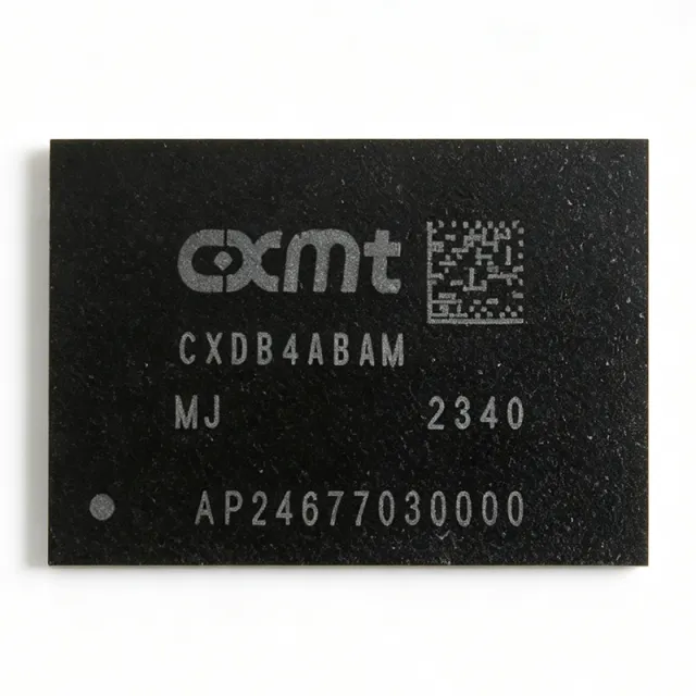
CXDB4ABAM - 2GB LPDDR4X SDRAM 3733Mbps | CXMT
CXDB4ABAM

CXDB4ABAM - 2GB LPDDR4X SDRAM 3733Mbps | CXMT

The CXDB4ABAM is a 2GB LPDDR4X SDRAM memory chip manufactured by ChangXin Memory Technologies (CXMT). It operates at a data rate of 3733 Mbps and is housed in a 200-ball FBGA package (15x10x0.8mm). This low-power double data rate memory is designed for mobile, embedded, and consumer applications requiring high bandwidth and low power consumption. LPDDR4X is a type of synchronous dynamic random-access memory (SDRAM) that is part of the LPDDR (Low Power Double Data Rate) family, which is optimized for battery-powered devices. It is a successor to LPDDR4 and offers reduced I/O voltage (0.6V) compared to LPDDR4 (1.1V), resulting in lower power consumption while maintaining similar performance. LPDDR4X is widely used in smartphones, tablets, ultra-thin laptops, and embedded systems where power efficiency is critical. Key features of the CXDB4ABAM include a 2GB density, 3733 Mbps data rate, and support for dual-channel operation. The device uses a 200-ball FBGA package with a 0.8mm ball pitch, enabling compact PCB designs. It is RoHS compliant and supports industrial temperature ranges, making it suitable for a variety of applications. The CXDB4ABAM utilizes advanced DRAM process technology to achieve high speed and low power. It supports various power-saving modes, including idle, self-refresh, and deep power-down, which are essential for extending battery life in portable devices. The memory interface is compatible with standard LPDDR4X controllers, simplifying integration into SoC designs. Typical applications include smartphones, tablets, embedded computing, AI edge devices, and automotive infotainment systems. The high bandwidth and low power make it ideal for applications requiring fast data processing and long battery life. When designing with the CXDB4ABAM, ensure proper decoupling and signal integrity practices are followed. The 0.6V I/O voltage requires careful PCB layout to minimize noise and maintain signal integrity at high data rates.

USD $19,09 Kontakt
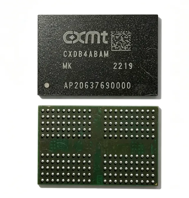
CXDB4ABAM-MK - 8Gb LPDDR4X SDRAM 3733MHz | CXMT
CXDB4ABAM-MK

CXDB4ABAM-MK - 8Gb LPDDR4X SDRAM 3733MHz | CXMT

The CXDB4ABAM-MK is a high-performance LPDDR4X SDRAM memory chip manufactured by ChangXin Memory Technologies (CXMT). It operates at a data rate of 3733 MHz, delivering high-speed data transfer for mobile and computing applications. The device is housed in a 200-ball FBGA package (BGA-200, 15x10x0.8 mm), which supports high-density PCB designs with efficient thermal performance. As an LPDDR4X device, it offers low power consumption, making it ideal for battery-powered devices. LPDDR4X (Low Power Double Data Rate 4X) is a type of synchronous dynamic random-access memory (SDRAM) designed for mobile and embedded systems. It is an evolution of LPDDR4, offering higher data rates and lower power consumption through reduced I/O voltage (0.6V). LPDDR4X is part of the broader DRAM memory hierarchy, which includes DDR4, DDR5, and LPDDR5, and is specifically optimized for power-sensitive applications such as smartphones, tablets, and IoT devices. Key features of the CXDB4ABAM-MK include a 3733 MHz data rate, 8Gb density, and support for dual-channel operation. The device operates from a 1.8V VDD1 and 1.1V VDD2 power supply, with a VDDQ of 0.6V for the I/O, reducing power consumption by up to 20% compared to LPDDR4. It supports various operating modes including active, standby, and deep power-down, enabling efficient power management. The package is RoHS compliant, meeting environmental standards. The CXDB4ABAM-MK utilizes advanced process technology to achieve high speed and low power. It features on-die termination (ODT) for improved signal integrity and supports a 16n prefetch architecture, which enhances data throughput. The device includes a temperature-compensated self-refresh (TCSR) mechanism to maintain data integrity across a wide temperature range. The 200-ball FBGA package provides excellent thermal dissipation and is suitable for space-constrained designs. Typical applications include smartphones, tablets, set-top boxes, and IoT devices. In smartphones, the high data rate enables smooth multitasking and immersive VR experiences. In set-top boxes, it supports high-definition video streaming and fast app loading. The low power consumption extends battery life in portable devices. When designing with this device, ensure proper decoupling capacitors are placed near the power pins to minimize noise. The device requires a stable power supply and careful PCB layout to maintain signal integrity at 3733 MHz. Refer to the datasheet for detailed layout guidelines.

USD $19,09 Auf Lager
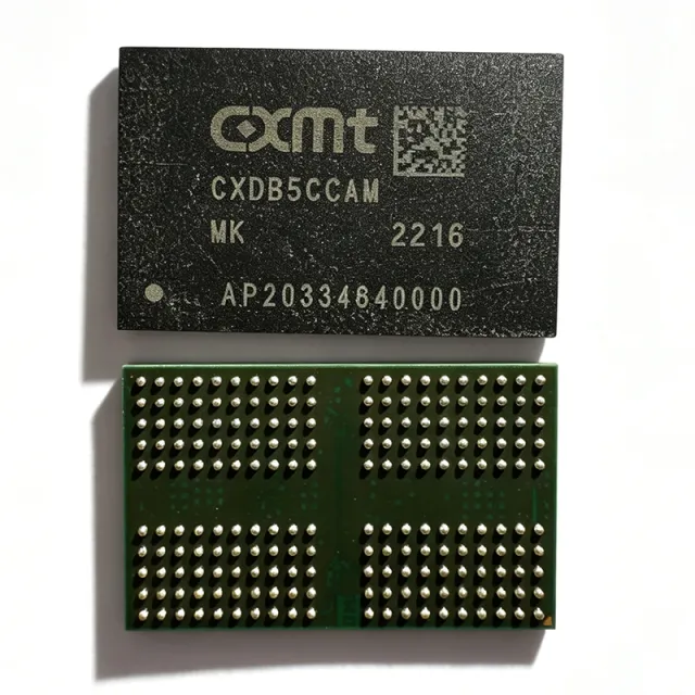
CXDB5CCAM-MK - LPDDR4X SDRAM 8Gb | CXMT | Mobile & AI
CXDB5CCAM-MK

CXDB5CCAM-MK - LPDDR4X SDRAM 8Gb | CXMT | Mobile & AI

The CXDB5CCAM-MK is a high-performance LPDDR4X SDRAM manufactured by ChangXin Memory Technologies (CXMT), designed for mobile, embedded, and AI applications requiring high bandwidth and low power consumption. It features a 200-ball BGA package (BGA200) and operates over a temperature range of -25°C to +85°C, making it suitable for a wide variety of consumer and industrial devices. LPDDR4X (Low Power Double Data Rate 4X) is a type of synchronous dynamic random-access memory (SDRAM) optimized for low power consumption and high data rates, commonly used in smartphones, tablets, and embedded systems. It is part of the LPDDR memory family, which evolved from DDR to provide reduced voltage and power for mobile applications. LPDDR4X operates at a lower I/O voltage (0.6V) compared to LPDDR4 (1.1V), enabling significant power savings while maintaining high bandwidth. Key features of the CXDB5CCAM-MK include support for asynchronous reset, data mask function, and ZQ calibration, which are essential for reliable memory operation. The device is RoHS compliant, ensuring environmental safety. The BGA200 package offers a compact footprint suitable for space-constrained designs, and the -25°C to +85°C operating temperature range supports both commercial and industrial applications. Technically, the CXDB5CCAM-MK is a 8Gb (gigabit) LPDDR4X device, organized as 512M x 16, providing a 16-bit data bus. It supports data rates up to 4266 Mbps, delivering high bandwidth for demanding applications. The memory uses a 1.1V core voltage and 0.6V I/O voltage, reducing power consumption by up to 40% compared to LPDDR4. The device includes on-die ECC and supports deep power-down mode for extended battery life. Typical applications include smartphones, tablets, AI edge devices, and automotive infotainment systems. The CXDB5CCAM-MK is also used in Rockchip RK3588S-based systems, where it provides the necessary memory bandwidth for high-resolution displays and AI processing. Its low power consumption makes it ideal for battery-powered devices. When designing with this memory, ensure proper PCB layout for high-speed signals, including impedance matching and minimal trace lengths. Use the ZQ calibration feature to optimize signal integrity. The device supports a wide range of operating conditions, but careful attention to power supply decoupling is recommended to maintain stable operation.

USD $54,09 Auf Lager
CY14101V - 1-Mbit Quad SPI nvSRAM | Infineon | Non-Volatile SRAM
CY14101V

CY14101V - 1-Mbit Quad SPI nvSRAM | Infineon | Non-Volatile SRAM

The Infineon CY14101V is a 1-Mbit non-volatile SRAM (nvSRAM) memory IC organized as 128K words x 8 bits, accessed through a high-speed Quad SPI (QPI) interface. According to the Infineon datasheet for the CY14V101QS family, this device combines a standard SRAM array with on-chip non-volatile storage cells that automatically save data on power loss, eliminating the need for backup batteries while sustaining full SRAM read/write performance. A Non-Volatile SRAM (nvSRAM) is a hybrid memory class that pairs a conventional SRAM cell array with a parallel non-volatile store (typically a SONOS or ferroelectric process) under the same die. On power-down the SRAM contents are autonomously recalled into the nvSTORE; on power-up they are restored to the SRAM cells, giving the engineer 'battery-free NVRAM' behavior. Within the broader taxonomy, nvSRAM sits between SRAM (volatile, fast, unlimited writes) and EEPROM/flash (non-volatile, slow write, page/block erase, limited endurance), giving nvSRAM byte-level writes at SRAM speeds with infinite endurance for the volatile side and >1 million STORE cycles for the non-volatile side. The CY14101V supports Single, Dual, and Quad SPI transfer modes, allowing up to four bits per clock cycle in Quad mode. The device operates as an SPI slave, with chip select (/CS), serial clock (SCK), and four I/O pins (IO0-IO3) for data transfer, plus a /HOLD pin for pausing serial communication. It is enabled through chip-select assertion and accessed using standard SPI opcodes including READ, WRITE, and status register commands. In typical operation the CY14101V delivers zero-cycle latency reads and writes up to 40 MHz in single/dual/quad modes, with optional 108-MHz operations introducing cycle latency on reads. The device includes a STORE-on-power-down watchdog, automatic RECALL on power-up, and an industry-standard 16-pin SOIC or 24-ball BGA footprint option across family variants. The CMOS process provides low standby current and unlimited read/write endurance for the SRAM array. Typical applications include data logging in industrial controllers, parameter retention in metering equipment, event capture in point-of-sale terminals, configuration storage in networking gear, and fail-safe scratchpad memory in medical instruments. The Quad SPI bus also suits high-throughput FPGA and DSP boot/log buffers where fast restore-after-reset is required. When designing with the CY14101V, ensure decoupling caps are placed within 5 mm of VDD with a low-ESR 0.1 uF parallel to a 4.7 uF bulk cap. The /HOLD and /WP pins must be tied to VIO (or driven by the host) to avoid unintended interruption of SPI operation. Verify that host SPI controller supports 1-, 2- and 4-bit modes required to leverage the full Quad throughput. This page synthesizes Infineon datasheet parameters, equivalent-drop-in alternative mapping across the CY14V101 family, and practical design notes not collated in the manufacturer datasheet alone.

Angebot Kontakt
CY14104V - IEEE 1149.1 Boundary-Scan Controller | Cypress
CY14104V

CY14104V - IEEE 1149.1 Boundary-Scan Controller | Cypress

The Cypress (Infineon) CY14104V is a 1.8V-3.3V IEEE 1149.1 / IEEE 1149.7 boundary-scan (JTAG) controller and TAP controller companion IC, offered in a low-pin-count surface-mount package (per published part numbering convention). According to the manufacturer datasheet, this device provides compliant TAP (Test Access Port) signaling, programmable TCK frequencies, and integrated TAP domain support for both 4-wire JTAG and the 2-wire compact JTAG (cJTAG) variant standardized in IEEE 1149.7. A boundary-scan controller is a category of test and measurement IC that orchestrates boundary-scan testing of digital logic on a printed circuit board. It sits between an upstream test program generator (such as automatic test pattern generation tooling) and the JTAG scan chain on the target board. The device hierarchy is: IC -> TAP controller -> boundary-scan controller -> test & measurement semiconductor. Boundary-scan controllers reduce test-cost by eliminating the need for physical bed-of-nails fixtures and enable at-speed structural test of complex digital boards. Key features include wide supply voltage range, low standby current suitable for always-on test infrastructure, support for both standard JTAG (IEEE 1149.1) and compact JTAG (IEEE 1149.7), and integrated programmable frequency generation for TCK. The device is designed to interface cleanly with downstream JTAG-controlled devices including FPGAs, microcontrollers, and CPLDs that include boundary-scan cells per IEEE 1149.x. Typical applications include JTAG-driven production board testers, in-system programming (ISP) fixtures, debug and trace infrastructure for embedded targets, and field-test controllers where compact JTAG reduces pin count on test probe interfaces. When designing with this part, follow IEEE 1149.1 signal-integrity guidelines: keep TCK and TMS traces short, route them above a continuous ground reference, and add 10k-100k pull-ups on TMS and TDI to set a benign idle state at power-up. This page synthesizes distributor pricing, drop-in alternatives, and practical JTAG design notes not found in the manufacturer datasheet, providing a single-page reference for engineers evaluating the CY14104V for production test fixtures or development JTAG bridges.

Angebot Kontakt
CY14B101J2-SXI - 1Mbit I2C nvSRAM 3.4MHz 8-SOIC | Infineon
CY14B101J2-SXI

CY14B101J2-SXI - 1Mbit I2C nvSRAM 3.4MHz 8-SOIC | Infineon

The Infineon CY14B101J2-SXI (originally Cypress Semiconductor) is a 1-Mbit serial nvSRAM non-volatile memory IC with 128K x 8 organization, a 3.4 MHz I2C interface, and 20-year data retention, housed in an 8-pin SOIC package. An nvSRAM (non-volatile static random access memory) is a hybrid memory device that combines the fast, unlimited-endurance read/write behavior of SRAM with the non-volatility of EEPROM or Flash. In the memory hierarchy, it sits between pure SRAM (volatile, fastest) and non-volatile technologies (EEPROM, FRAM, Flash), offering byte-wide SRAM access backed by automatic non-volatile store operations. This makes nvSRAM a power-management IC companion component in systems that must preserve state across power loss without the slow write cycles and limited endurance of EEPROM. Key features of the CY14B101J2-SXI include a 1-Mbit (128K x 8) array density, a standard two-wire I2C serial interface clocked at up to 3.4 MHz in high-speed mode, and guaranteed 20-year non-volatile data retention. Writes to the SRAM cell occur at SRAM speed with effectively unlimited endurance, while non-volatile store operations are software or hardware triggered using an external VCAP capacitor for energy harvesting during STORE. Architecturally, the device integrates a static RAM array with a non-volatile quantum-trap storage element per cell. During a STORE operation, data is transferred from the SRAM array into the non-volatile cells using energy drawn from the external VCAP capacitor, so the operation completes even if VCC has already been lost. On power-up, a RECALL operation automatically restores SRAM contents from the non-volatile array. Typical applications include industrial data loggers, metering systems, network equipment configuration storage, point-of-sale terminals, and robotic or factory-automation controllers where frequent state saving and instant power-loss protection are required. The I2C interface minimizes pin count, board area, and controller GPIO usage. When designing with this device, allocate board space for the external VCAP capacitor and follow the datasheet layout guidance; omitting or undersizing VCAP compromises STORE reliability. Also observe I2C bus pull-up sizing for 3.4 MHz high-speed operation. This page synthesizes verified distributor data, lifecycle information, drop-in alternative analysis, and practical design notes not found in the manufacturer datasheet, giving engineers a single citable reference for selection and sourcing decisions.

Angebot Kontakt
CY14B101J2-SXIT - 1Mb I2C nvSRAM, 3.4MHz SOIC-16 | Infineon
CY14B101J2-SXIT

CY14B101J2-SXIT - 1Mb I2C nvSRAM, 3.4MHz SOIC-16 | Infineon

The Infineon CY14B101J2-SXIT is a 1-Mbit (128K x 8) serial I2C nvSRAM (non-volatile SRAM) memory IC operating at 3.0V core with 3.4 MHz I2C clock frequency, housed in a 16-pin SOIC (0.300 inch, MO-119) surface-mount package originally developed by Cypress Semiconductor and now part of Infineon Technologies. nvSRAM is a class of non-volatile RAM that combines the fast, unlimited read/write behavior of SRAM with the non-volatility of EEPROM or Flash. The device hierarchy places nvSRAM under non-volatile memory, which in turn sits under memory ICs and semiconductor devices. Unlike EEPROM, which requires slow erase/write cycles with limited endurance, nvSRAM stores data in a conventional SRAM cell and automatically transfers (STOREs) it to a non-volatile quantum-trap storage element on power failure, command, or brown-out, achieving effectively infinite SRAM read and write cycles. Key features include 1-Mbit density organized as 128K words of 8 bits, a standard two-wire I2C serial interface operating up to 3.4 MHz, infinite read, write, and RECALL cycles, and automatic STORE on power loss with data retention specified for 20 years. These specifications make the device suitable for write-intensive data logging where EEPROM endurance would be a bottleneck. Technically, the nvSRAM architecture pairs each SRAM cell with a non-volatile capture element; the part handles STORE and RECALL internally, including thermal management of the store operation, requiring an external reservoir capacitor (VCAP) to power the store during power failure. The I2C interface simplifies board routing to just two signal lines (SDA, SCL) plus power and ground. Typical applications include industrial data loggers, metering equipment, network switches storing configuration tables, and point-of-sale or POS terminals requiring frequent writes to non-volatile memory. The -40C to +85C industrial temperature range supports harsh deployments. Design consideration: always size and specify the VCAP reservoir capacitor per the manufacturer datasheet; an undersized capacitor risks data loss during STORE on power-down. This page synthesizes distributor pricing, drop-in family alternatives, and practical design notes beyond the raw datasheet.

Angebot Kontakt
CY14B101KA-SP25XIT - 1Mbit nvSRAM 25ns with RTC | Infineon
CY14B101KA-SP25XIT

CY14B101KA-SP25XIT - 1Mbit nvSRAM 25ns with RTC | Infineon

The Infineon (Cypress Semiconductor) CY14B101KA-SP25XIT is a 1-Mbit non-volatile static RAM (nvSRAM) organized as 128K x 8 with an integrated real-time clock (RTC), delivering a fast 25 ns access time on a 2.7V to 3.6V supply in a 48-pin SSOP surface-mount package. An nvSRAM (non-volatile SRAM) is a memory device that combines the infinite read/write endurance and fast random access of static RAM with the non-volatility of EEPROM or Flash. In the memory hierarchy, it sits between SRAM (volatile, fast) and Flash/EEPROM (slow writes, limited endurance). Cypress QuantumTrap nvSRAM stores an automatic copy (AutoStore) of the SRAM contents into non-volatile QuantumTrap cells on power loss, requiring no external capacitor for store operations in this family, and restoring data on power-up. Key features include the 25 ns parallel SRAM access time, unlimited SRAM read/write endurance, 20-year non-volatile data retention, and a full-featured RTC with alarm and a backup power capability. The monolithic integration of nvSRAM plus RTC eliminates a separate RTC chip and battery-backed SRAM module, reducing board area and failure points. Architecturally, the device merges a fast SRAM core with QuantumTrap nonvolatile elements; data resides in SRAM during normal operation while a nonvolatile shadow copy is maintained or committed via store events (hardware, software, or AutoStore on power-down). Write protection and hardware store (HSB) pins support safe power-fail management. Typical applications include industrial data loggers, PLCs and factory automation controllers, network equipment configuration storage, metering systems, and avionics/medical equipment requiring fast non-volatile scratchpad memory plus accurate timekeeping. Design consideration: guarantee the supply sequencing and observe the minimum VCC detect thresholds so AutoStore completes during brown-out; ensure the HSB pin is properly pulled up per the manufacturer datasheet. This page synthesizes distributor pricing, drop-in same-family alternatives, and practical design notes not found in the manufacturer datasheet.

Angebot Kontakt
CY14B104NA - 4Mbit 256Kx16 nvSRAM 25ns | Infineon/Cypress
CY14B104NA

CY14B104NA - 4Mbit 256Kx16 nvSRAM 25ns | Infineon/Cypress

The Cypress Semiconductor (now Infineon Technologies) CY14B104NA is a 4-Mbit nonvolatile static RAM (nvSRAM) organized as 256K x 16 bits, with a 25 ns access speed grade available, housed in a 44-pin TSOP II or 54-ball FBGA package. An nvSRAM is a memory IC that pairs a standard SRAM cell with a nonvolatile QuantumTrap element in each bit cell. Within the memory hierarchy it sits between pure SRAM (fast but volatile) and EEPROM/Flash (nonvolatile but slow to write). nvSRAM behaves like fast SRAM during normal operation and copies the entire array into the nonvolatile elements on power-down or on demand, so no battery backup is required. Key features include three storage operations: hardware STORE triggered by the HSB pin, software STORE via an address sequence, and AutoStore on power-down (enabled by default). Access times of 20 ns, 25 ns, and 45 ns are offered across the family. Write operations are SRAM-fast, giving effectively unlimited endurance during SRAM operation, while the nonvolatile element retains data for years without power. The device is built on Cypress QuantumTrap technology, which uses a proprietary trapping-layer process to capture charge in each cell without the erase/write bottlenecks of Flash. During low-voltage conditions (VCC below VSWITCH), the device inhibits all externally initiated STORE and write operations to protect data integrity from corruption. Typical applications include industrial PLCs and data loggers, RAID/disk-drive controller configuration storage, networking equipment for fast-reboot state retention, and automotive event recorders where the automotive-qualified CY14B104NA variants apply. Design consideration: the 8 ms (typical family value) STORE operation temporarily blocks SRAM access, so firmware should tolerate a short stall on power-down and reserve adequate hold-up capacitance to complete AutoStore. This page synthesizes distributor pricing, verified cross-reference data including the Everspin MRAM drop-in equivalent, and practical design notes not consolidated in the manufacturer datasheet.

Angebot Kontakt
CY14V104LA - 4Mb Parallel nvSRAM 3.3V 48-FBGA | Infineon
CY14V104LA

CY14V104LA - 4Mb Parallel nvSRAM 3.3V 48-FBGA | Infineon

The Infineon CY14V104LA is a 4-Mbit (512K x 8 / 256K x 16) non-volatile SRAM (nvSRAM) that combines a fast static RAM cell array with a non-volatile storage element in every memory cell, offered in a 48-ball Fine-pitch BGA (6 x 10 mm) package. The device operates from a 3.3 V supply (3.0 V to 3.6 V) and is available in 25 ns and 45 ns access-time grades, providing SRAM-comparable read/write performance with automatic non-volatile backup on power loss. An nvSRAM (non-volatile SRAM) is a hybrid memory class that pairs standard SRAM cells (typically 6T) with a non-volatile element per cell - either a small SONOS-style charge trap or an EEPROM/FRAM-like element - so that on VCC drop the entire contents can be stored to the non-volatile layer in microseconds, then restored on the next power-up. Compared with pure SRAM, nvSRAM eliminates external battery, supercapacitor, or EEPROM-shadow designs; compared with serial EEPROM or FRAM, it offers true parallel bus access and unlimited read endurance. nvSRAMs sit in the memory hierarchy between SRAM (highest speed, volatile) and Flash (non-volatile, slow write), targeting applications needing deterministic, high-speed writes without data-loss risk. Key features include 4-Mbit density organized as 512 Kbytes x 8 or 256 Kwords x 16 (selectable by the /BYTE pin), hardware STORE-on-power-loss using an integrated threshold-detect circuit, automatic RECALL on power-up, and an unlimited SRAM-side read/write endurance typical of static RAM. The parallel interface uses standard JEDEC-style control signals (CE#, OE#, WE#, UB#, LB#) so it can drop into existing SRAM or battery-backed SRAM sockets. The 48-FBGA package is 6 x 10 x 1.20 mm and is RoHS compliant. Internally the CY14V104LA integrates the SRAM array, the non-volatile element, an on-chip STORE capacitor (no external cap required for energy-limited store), voltage-compare and STORE-control logic, and a software-invoked STORE (HSB pin). The architecture enables 0.7 ms typical STORE time and 0.7 ms typical RECALL time while drawing Icc of about 65 mA active and Isb of about 5 mA standby. The 25 ns grade (-BA25XI suffix) delivers faster system clocks; the 45 ns grade (-BA45XI suffix) targets lower-cost industrial systems. Typical applications include industrial controllers, programmable logic controllers (PLC), factory automation data loggers, point-of-sale (POS) terminals, metering, RAID controllers, and gaming equipment. The wide -40 C to +85 C industrial temperature range and automatic power-loss protection make the CY14V104LA particularly suited for systems that must survive brown-outs and uncontrolled power-down events without user intervention. When designing with the CY14V104LA, route the parallel bus with matched trace lengths, keep CE#, OE#, WE# cleanly decoupled to avoid accidental STORE triggering, and follow the datasheet ground-bounce and decoupling recommendations for the 48-FBGA footprint. Note that STORE operations are non-maskable by design - power-supply decoupling directly affects STORE reliability. This page synthesizes distributor pricing, drop-in alternatives, and practical design notes for the CY14V104LA in a single reference not found in the bare datasheet, including the parametric comparison with the CY14V104NA x16-only and CY14B104L family variants.

Angebot Kontakt
CY14V104LA-BA25XI - 4Mbit nvSRAM 25ns FBGA-48 | Infineon
CY14V104LA-BA25XI

CY14V104LA-BA25XI - 4Mbit nvSRAM 25ns FBGA-48 | Infineon

The Infineon Technologies CY14V104LA-BA25XI (originally Cypress Semiconductor) is a 4-Mbit non-volatile SRAM (nvSRAM) organized as 512K x 8 or 256K x 16, with a fast 25 ns access time, 1M STORE cycles, and 20-year non-volatile data retention, housed in a 48-ball FBGA (6 x 10 mm) package rated for -40C to +85C industrial operation. An nvSRAM is a memory IC that combines the fast, unlimited read/write endurance of a standard static RAM with a non-volatile element in each memory cell. In the broader memory hierarchy, nvSRAM sits between volatile SRAM and EEPROM/Flash: it behaves like a parallel SRAM during normal operation but automatically stores the SRAM contents to non-volatile cells on power loss, eliminating the need for external batteries. Key features include the 25 ns access time for zero-wait-state parallel bus designs, automatic STORE on power-down triggered by the hardware STORE (HSB) pin, a minimum 1 million STORE cycle endurance, and 20-year data retention at 85C. The dual organization (byte-wide via x8 mode and word-wide via x16 with byte enables BHE/BLE) lets one design cover both 8-bit and 16-bit buses. Technically, the CY14V104LA performs SRAM reads when CE and OE are LOW and WE and HSB are HIGH; addresses A0-A18 (x8) or A0-A17 (x16) select among 524,288 bytes or 262,144 words. The RECALL function restores non-volatile data to SRAM at power-up, and software-triggered STORE/RECALL sequences are supported via address sequences per the Infineon/Cypress datasheet. Typical applications include industrial PLCs and data loggers, networking equipment configuration storage, medical instrumentation, and automotive/avionics black-box buffers where a sudden power loss must not corrupt data. Design consideration: reserve a small capacitor energy margin on the 3.3V rail so the device can complete a hardware STORE event during brownout; the HSB pin should be monitored or driven by supervisory logic to guarantee the STORE window. This page synthesizes verified distributor pricing, drop-in family alternatives, and practical design guidance not found in the standard datasheet extract, with all data marked with its last-verified date for freshness.

Angebot Kontakt
CY23EP09SXI-1HT - 220MHz 9-Output Zero Delay Buffer | Infineon
CY23EP09SXI-1HT

CY23EP09SXI-1HT - 220MHz 9-Output Zero Delay Buffer | Infineon

The Infineon CY23EP09SXI-1HT is a 2.5V/3.3V nine-output zero delay buffer (ZDB) integrated circuit designed to distribute high-speed clocks across digital systems. Operating over a 10 MHz to 220 MHz range at 3.3V (200 MHz at 2.5V), the device uses an on-chip PLL to lock to a reference clock on the REF pin and provides zero input-to-output propagation delay. The feedback is taken internally from the CLKOUT pad, eliminating the need for external feedback routing. It is housed in a 16-pin SOIC (0.154 inch, 3.90 mm width) industrial-grade package, supplied on Tape & Reel. A zero delay buffer (ZDB) is a type of clock fanout/distribution IC that uses a phase-locked loop (PLL) to ensure the output clock edges remain aligned with the input reference clock edge, achieving sub-nanosecond skew. ZDBs sit in the clock distribution hierarchy between a primary oscillator or PLL clock generator and the downstream loads (CPUs, FPGAs, ASICs, DDR memory, serializers). They belong to the broader clock-and-timing category of integrated circuits and are widely used to multiply clock fanout without introducing timing drift. Key features of the CY23EP09SXI-1HT include 9 low-skew outputs, 45 ps typical output-to-output skew, an on-chip PLL with internal feedback, and a -1H higher-drive variant compared to standard -1 devices. The device supports industrial operating temperature ranges and is qualified for fanout buffer applications where low jitter and matched propagation delays are required across multiple loads. The CY23EP09SXI-1HT is widely used in networking line cards, server motherboards, storage controllers, and telecommunications infrastructure as a clock distribution element. The 'I' suffix in the MPN denotes industrial temperature grade, while 'T' indicates Tape & Reel packaging. It is pin-compatible with the broader CY23EP09 family, allowing board designers to swap standard and -1H drive variants without layout changes. When designing with this device, ensure the REF input clock meets the PLL lock range and that decoupling capacitors are placed close to VDD pins. Output load matching is critical to maintain skew performance across the nine outputs.

Angebot Kontakt
CY62148ESL-55ZAXI - 4Mb 55ns Async SRAM 32-STSOP | Infineon
CY62148ESL-55ZAXI

CY62148ESL-55ZAXI - 4Mb 55ns Async SRAM 32-STSOP | Infineon

The Infineon CY62148ESL-55ZAXI is a 4-Mbit (512K × 8) asynchronous static RAM organized as 512K words of 8 bits, with 55 ns access time, supplied in a 32-pin STSOP (Standard Thin Small Outline Package, Type I) and operating from 2.2 V to 5.5 V. It delivers ultra-low active power and deep power-down currents, with CMOS-compatible I/O that interfaces directly to TTL levels. A static RAM (SRAM) is a volatile semiconductor memory that retains data as long as power is applied without requiring refresh cycles, in contrast to dynamic RAM (DRAM). Within the memory hierarchy, SRAM sits above DRAM in performance — measured in nanosecond access times versus tens of nanoseconds for synchronous DRAM — at the cost of density per die area. The CY62148ESL belongs to the low-power SRAM family, used as cache, scratchpad, buffer or boot memory in embedded systems. Key features of the CY62148ESL-55ZAXI include an industry-standard SRAM pinout (JEDEC-compatible) with active-high Chip Enable (CE1) and active-low Chip Enable (CE2) plus Output Enable (OE) and Write Enable (WE) controls, automatic power-down when deselected, and low standby current. The 32-pin STSOP-I footprint is the JEDEC-standardized small-outline thin package widely accepted for space-constrained portable designs. Technically, the CY62148ESL uses a 6-transistor CMOS memory cell with full CMOS I/O buffers, giving the device its TTL-compatible input thresholds. The 55 ns access time corresponds to the part number suffix -55, while the 'SL' family designation indicates the MoBL (More Battery Life) ultra-low-power architecture acquired from Cypress Semiconductor by Infineon. Typical applications include battery-backed portable equipment, cellular phones, pagers, handheld POS terminals, industrial controls, networking line cards, automotive infotainment subsystems and any system that requires non-volatile configuration storage behind a coin-cell backup. The 2.2 V to 5.5 V range covers single-cell Li-ion (2.7-4.2 V), 3.3 V logic rails and legacy 5 V designs from the same silicon. When designing, place a 0.1 µF decoupling capacitor close to each VCC pin and provide a ground plane beneath the package to control I/O switching noise. Verify that CE1, CE2 and WE timing satisfy the datasheet write-cycle constraints when used as boot ROM. This page synthesizes distributor pricing, drop-in JEDEC-compatible 32-STSOP alternatives and practical design notes not found in the standalone manufacturer datasheet, enabling faster part selection for low-power embedded memory designs.

Angebot Kontakt
CY62167EV30LL-45BVXI - 16Mb SRAM 45ns 1M×16/2M×8 VFBGA-48 | Infineon
CY62167EV30LL-45BVXI

CY62167EV30LL-45BVXI - 16Mb SRAM 45ns 1M×16/2M×8 VFBGA-48 | Infineon

The Infineon CY62167EV30LL-45BVXI is a 16-Mbit (1M × 16 or 2M × 8 configurable) ultra-low-power CMOS static RAM organized as a parallel asynchronous memory with a 45 ns access time, packaged in a 48-ball VFBGA (6 × 8 × 1 mm) outline. Operating from a wide 2.2 V to 3.6 V single supply, the device belongs to the MoBL® family and delivers typical active current of approximately 2 mA at 1 MHz, making it a strong fit for battery-backed and energy-constrained designs. The ball-grid package keeps the PCB footprint extremely small while still exposing a full 16-bit data bus. An asynchronous SRAM (static random-access memory) is a volatile memory that retains data as long as power is applied, without needing refresh cycles. It occupies the memory IC tier of the hierarchy: SRAM -> volatile memory -> memory IC -> semiconductor. Compared with DRAM, SRAM trades density for speed and simplicity, which is why it is favored for cache, FIFOs, and working buffers in embedded systems. The MoBL® process technology used in the CY62167EV30 family achieves very low active current (2 mA at 1 MHz typical) and ultra-low standby current. A BYTE pin on the 48-ball BGA allows the user to organize the array as 1M × 16 (BYTE = VCC) or 2M × 8 (BYTE = VSS). Standard features include chip-enable (CE1#, CE2), output enable (OE#), and write enable (WE#) controls, supporting common asynchronous read/write protocols. The 45 ns access time is well-suited to mid-speed microcontrollers, ASICs, and DSPs that do not require synchronous burst interfaces. The VFBGA-48 (BV48) package provides a small 6 mm × 8 mm footprint suitable for handheld and space-limited designs. Multiple temperature grades are offered within the family (industrial -40 °C to +85 °C and automotive variants), and the part is Pb-free / RoHS compliant. Typical applications include industrial handheld terminals, point-of-sale (POS) terminals, automotive infotainment buffers, networking line cards, and battery-backed metering or instrumentation buffers where data retention must survive short power interruptions. When designing with the CY62167EV30LL-45BVXI, observe proper decoupling (0.1 µF + 1 µF near VCC) and avoid lengthy traces to the data bus to minimize bus-turnaround skew. For lower-power standby, drive CE1# high during idle periods and CE2 low to enter standby mode. This page synthesizes distributor stock, drop-in alternatives and design guidance not consolidated on the manufacturer product page.

Angebot Kontakt
CY62168EV30LL-45BVXI - 16Mb SRAM 45ns 3V | Infineon
CY62168EV30LL-45BVXI

CY62168EV30LL-45BVXI - 16Mb SRAM 45ns 3V | Infineon

The Infineon CY62168EV30LL-45BVXI is a 16-Mbit (2M × 8) asynchronous static RAM (SRAM) with 45 ns access time, operating from 2.20 V to 3.60 V, housed in a 48-ball VFBGA (6x8) package. It belongs to the MoBL (More Battery Life) ultra-low-power SRAM family originally developed by Cypress Semiconductor, which is now part of Infineon Technologies. The device delivers high-speed asynchronous read/write access with very low active and standby currents, making it ideal for battery-powered and portable designs. An asynchronous SRAM is a type of volatile memory that does not require a clock for core read and write operations - the address and chip-enable signals directly control access. SRAM sits in the memory hierarchy above DRAM (no refresh needed) and below CPU registers (larger but slower than on-chip cache). The CY62168EV30LL falls into the low-power SRAM category, which trades absolute speed for ultra-low quiescent current to extend battery life in mobile equipment. Key features include very high-speed 45 ns access, 2.2 V to 3.6 V wide voltage range, ultra-low standby power with typical standby current of 1.5 µA (maximum 12 µA), and ultra-low active power with typical active current of 2.2 mA at 1 MHz. The device offers easy memory expansion with active-low CE1 and CE2 chip-enable inputs, automatic power-down when deselected, and CMOS-compatible I/O. The 48-VFBGA (6x8) package is optimized for compact surface-mount designs. The CY62168EV30LL-45BVXI uses a 6-transistor (6T) CMOS SRAM cell architecture with asynchronous address-latch and sense-amplifier circuitry. Its internal organization is 2 M × 8 bits with common I/O data lines and byte-wide access via CE1/CE2 control. The wide voltage range and low-power architecture are achieved through a 0.13 µm low-leakage process and dynamic power management circuits that monitor CE1/CE2 activity. Typical applications include portable media players, handheld GPS units, cellular phone buffers, PDAs and data-acquisition devices, handheld instruments, battery-powered systems, and cellular phone base-band buffering. It also fits industrial low-power data logging and embedded systems that require non-DRAM memory with deterministic low-latency reads. When designing with this device, ensure that VCC decoupling (0.1 µF + 1 µF ceramic) is placed within 5 mm of the supply pins. Because it is a BGA package, proper PCB pad design, reflow profile (per JEDEC J-STD-020), and X-ray inspection are mandatory for reliable assembly. Note that the 45 ns speed grade is conservative for moderate-performance buffering; for higher bandwidth consider the CY62168G30 family. This page synthesizes Infineon/Cypress datasheet specifications, distributor stock and pricing, drop-in and same-package alternatives, and practical PCB/thermal design notes not found in the manufacturer datasheet alone.

Angebot Kontakt
CY7C1021DV33-10BVXIT - 1Mbit (64Kx16) 10ns Async SRAM | Infineon
CY7C1021DV33-10BVXIT

CY7C1021DV33-10BVXIT - 1Mbit (64Kx16) 10ns Async SRAM | Infineon

The Infineon CY7C1021DV33-10BVXIT is a high-performance CMOS asynchronous Static RAM (SRAM) organized as 65,536 words by 16 bits (1 Mbit), with a 10 ns access time, housed in a 48-ball VFBGA (6x8) package and supplied on Tape & Reel. It operates from a single 3.0 V to 3.6 V supply and is offered in the industrial temperature grade with the "IT" suffix. An asynchronous SRAM (static random-access memory) is a high-speed volatile memory that does not require a clock signal - read and write operations are triggered directly by chip-enable (CE), output-enable (OE), and write-enable (WE) inputs. SRAM sits in the memory hierarchy above DRAM for speed and below cache for cost/density, and the asynchronous (or "async" part forms the typical choice for direct-mapped buffers in microcontroller and DSP systems. The CY7C1021DV33 family adds an automatic power-down feature that drops ICC to a few microamps when deselected, making it well-suited to battery-powered or power-aware industrial systems. Key features of the CY7C1021DV33-10BVXIT include 10 ns address access time, 10 ns output enable access time, JEDEC-compatible center-power/center-ground pinout, TTL-compatible I/O, and equal read/write cycle times. The 48-VFBGA (6x8) package is only 6x8 mm, giving the densest footprint option in the family alongside the 44-pin 400-mil SOJ and 44-pin TSOP II packages - all sharing the same functional pinout per JEDEC standard. Typical applications include industrial control buffers, networking line cards, automotive infotainment buffers, point-of-sale terminals, set-top box working memory, and microcontroller/DSP scratch-pad memory. The wide x16 data bus minimizes glue logic when paired with 16-bit microcontrollers such as the 80C186, 68HC16, and DSP families. When designing with this device, place a 0.1 uF decoupling capacitor on each VCC/ground pair and follow JEDEC standard PCB layout for 48-VFBGA. The automatic power-down feature reduces standby current to 5 mA typical when CE# is high; use this to extend battery life in portable designs.

Angebot Kontakt
CY7C65100-SC - 4-Port USB 1.1 Hub Controller | Infineon
CY7C65100-SC

CY7C65100-SC - 4-Port USB 1.1 Hub Controller | Infineon

The Infineon CY7C65100-SC is a fixed-function four-port USB hub controller with 8 kB of OTP program memory, USB 1.1 compliance, and a 28-pin SOIC package measuring 0.295 inch, or 7.50 mm, wide. It expands one upstream USB attachment point into as many as four downstream ports without requiring firmware development. According to the manufacturer datasheet, the device is designed as a self-contained USB hub solution that reduces design risk and simplifies implementation. What is a USB hub controller? A USB hub controller is an interface IC that manages traffic between one upstream host connection and multiple downstream USB peripherals. In the device hierarchy, it belongs to the USB interface controller family, then interface integrated circuits, and finally semiconductors. Fixed-function controllers implement standard hub behavior in hardware rather than relying on application firmware, making them useful for established USB expansion designs. The CY7C65100 series supports USB Specification Revision 1.1 and provides up to four downstream ports. Its fixed-function architecture removes firmware-development requirements, while its 8 kB OTP memory provides embedded program storage. The 28-pin SOIC package supports conventional surface-mount assembly, and distributor records identify the device as an application-specific USB hub or microcontroller IC. The controller is intended for computers and peripheral systems that need additional USB attachment points. Typical implementations include desktop USB expansion, computer peripherals, external connection accessories, and legacy USB 1.1 equipment. Its four-port capability consolidates multiple downstream links behind one upstream port, reducing the need for separate hub hardware when downstream port count is the primary requirement. Engineers should verify the complete electrical characteristics, pin names, timing limits, and USB signal-routing requirements in the manufacturer datasheet before layout. USB differential pairs require controlled impedance and careful branch geometry, particularly when four downstream ports share one upstream interface. Decoupling and power distribution should follow the datasheet recommendations, and enumeration behavior must be checked against the target host and connected devices. This page distinguishes verified product facts from parameters that require engineering confirmation. The manufacturer datasheet identifies fixed-function USB hub behavior, USB 1.1 compliance, four downstream ports, and no firmware-development requirement; detailed operating limits, electrical values, and exact pin assignments remain subject to the published technical data.

Angebot Kontakt
CY7C65113A-SXC - 4-Port USB Hub Controller | Infineon
CY7C65113A-SXC

CY7C65113A-SXC - 4-Port USB Hub Controller | Infineon

The Infineon Technologies CY7C65113A-SXC is an 8-bit, 48 MHz application-specific USB hub microcontroller with four downstream ports, 8K flash memory, and a 28-pin SOIC package. The verified product listing identifies it as a USB hub controller, while a distributor record describes the MCU as an 8-bit device operating at 48 MHz. Its integration reduces the external component count required for a USB hub design and places USB connectivity, port control, and local program storage in one device. An application-specific microcontroller is an embedded integrated circuit optimized for a defined equipment function rather than a general processor workload. Within the semiconductor hierarchy, this device belongs to the microcontroller family and specifically serves as a USB hub controller. Its 48 MHz processing capability supports USB traffic handling and hub-management logic, while the four-port configuration targets hubs that fan one upstream USB connection to multiple downstream devices. The verified listing identifies a 28-SOIC package and tube packaging. The package provides a surface-mount implementation compatible with conventional PCB assembly, and the SOIC form factor supports automated manufacturing while exposing more component leads than compact packages. The recorded 8K memory figure describes the device's on-chip program storage context, while the exact memory organization and programming interface require confirmation from the manufacturer datasheet. Typical uses include USB hubs, desktop peripherals, computer accessories, and embedded USB expansion equipment. In a hub design, the controller connects an upstream USB port to four downstream ports and manages downstream attach, detach, reset, and enumeration behavior under firmware control. The application-specific architecture can simplify board design compared with a discrete hub controller plus separate microcontroller arrangement, provided the design uses the manufacturer's reference firmware and electrical guidance. Engineers should verify the complete pinout, USB electrical limits, clock requirements, power sequencing, and firmware compatibility before layout because those details are not present in the supplied search data. A replacement must use the same 28-SOIC footprint and preserve pin functions, firmware behavior, voltage levels, timing, and USB compliance; a matching package name alone does not establish drop-in compatibility. This page consolidates verified sourcing information, package data, application context, and replacement-selection guidance rather than inferring unprovided electrical specifications.

Angebot Kontakt
CY7C65113C-SXC 48MHz USB Hub MCU | Infineon
CY7C65113C-SXC

CY7C65113C-SXC 48MHz USB Hub MCU | Infineon

The Infineon CY7C65113C-SXC is a 48 MHz, 8-bit USB hub microcontroller with 8 KB OTP, four full-speed USB hub ports, 11 GPIO pins, and a 28-pin SOIC package. Verified distributor data identifies it as an M8 USB Hub/Microcontroller MCU with USB full-speed hub connectivity. Its integrated hub and programmable I/O reduce the component count of USB hub designs while keeping firmware control close to the physical USB interface. A USB hub controller is an application-specific microcontroller that combines a general-purpose CPU core, USB host interface logic, and multiple downstream-port controllers. Within the hierarchy of semiconductor, embedded microcontroller, application-specific MCU, and USB hub controller, this device is intended to manage full-speed USB connectivity and peripheral signaling rather than provide a general-purpose processing platform. Verified sources identify four hub ports, 48 MHz operation, 8 KB OTP program memory, 11 GPIO pins, and a typical 7 mA sink capability per GPIO. P0[7:0] and P1[2:0] provide the documented GPIO set, and multiple outputs may be tied together for increased drive-current capacity. The SOIC-28 package is identified as 0.295 inch, or 7.50 mm, wide. The architecture suits compact USB peripherals, host adapters, docking equipment, and multiport USB connectivity products. Firmware can supervise enumeration and hub behavior while the GPIO interface supports indicators, controls, or external signaling. Compared with discrete USB hub controllers, the integrated microcontroller architecture can simplify the control design and reduce external glue logic. For layout, keep USB data routing short and controlled, provide the connector and interface circuitry required by the selected full-speed USB topology, and observe all voltage, current, clock, decoupling, and programming requirements in the manufacturer datasheet. Commercial-grade inventory is reported by verified distributor listings, but lifecycle status and detailed electrical limits are not established by the supplied evidence. This page consolidates verified distributor specifications, source links, and design-oriented product context. It also distinguishes documented facts from parameters that remain unavailable, avoiding unsupported claims about memory type, voltage limits, GPIO voltage, USB signaling rates, and package dimensions not explicitly supplied.

Angebot Kontakt
CY7C65113C-SXCT 12Mbps 4-Port USB Hub | Infineon
CY7C65113C-SXCT

CY7C65113C-SXCT 12Mbps 4-Port USB Hub | Infineon

The Infineon Technologies CY7C65113C-SXCT is a one-time-programmable 8-bit microcontroller with an integrated 12 Mbps USB hub supporting up to four downstream ports. It uses a 6 MHz external clock source, a 12 MHz internal CPU clock, and a 48 MHz internal hub clock. The device is supplied in a 28-pin SOIC package measuring 0.295 inches, or 7.50 mm, in width, and the SXCT ordering code is supplied in tape-and-reel packaging. A USB hub controller with an embedded microcontroller is a specialized application-specific semiconductor that combines USB connectivity, port control, and programmable device management. Within the broader hierarchy, this device belongs to microcontrollers, USB interface integrated circuits, interface ICs, and semiconductors. Its Harvard-architecture instruction set was optimized specifically for USB operations, while retaining applicability to non-USB embedded-control functions. The principal feature is a full-speed USB hub integrated with a one-time-programmable 8-bit CPU. Verified source material identifies 8 KB of OTP program memory, four downstream-port support, 12 Mbps operation, a 6 MHz external clock, a 12 MHz internal CPU clock, and a 48 MHz internal hub clock. These parameters make it appropriate for compact USB hub, peripheral-control, and embedded USB-management designs where one device must perform both hub and local control functions. The device uses a Harvard architecture, separating the program and data organizations to support USB-oriented execution. Its one-time-programmable memory fixes the implemented firmware at production programming time. This characteristic can simplify secure configuration for dedicated USB products, but it also means design changes may require another programmed part rather than a simple field firmware update. Typical uses include four-port full-speed USB hubs, USB peripheral controllers, host-assisted downstream-port management, and compact embedded USB adapters. In a hub design, the downstream ports coordinate device attachment and enumeration, while the integrated microcontroller can manage board-specific functions. External USB transceivers, protection components, connectors, passives, and decoupling networks should be selected according to the system-level USB design requirements. PCB layout should keep USB data routing short, controlled, and away from noisy switching nodes. Follow the manufacturer datasheet for package dimensions, pin assignments, clock connections, decoupling, and programming. The SXCT package is 28-pin SOIC, so its footprint must match a 28-pin gull-wing layout rather than a leadless package. Commercial sourcing data and the manufacturer datasheet should be reviewed before approving a new design. This page consolidates verified distributor specifications, official-datasheet excerpts, package data, application guidance, and replacement-status analysis. Its practical value is that it distinguishes true device options from unsupported cross-reference results and highlights the OTP, clock, USB, and package constraints that most often determine design reuse.

Angebot Kontakt