Produkte (39.000+)

K4M56163PG-BG75 - 128Mb Mobile SDRAM, 16Mx16, 54-FBGA | Samsung
K4M56163PG-BG75

K4M56163PG-BG75 - 128Mb Mobile SDRAM, 16Mx16, 54-FBGA | Samsung

The Samsung K4M56163PG-BG75 is a 128 Mbit (4M x 16Bit x 4 Banks) Mobile Synchronous DRAM (SDRAM) organized as 16M words x 16 bits across four internal banks, housed in a 54-ball Fine-pitch Ball Grid Array (FBGA) package with a 1.8 V power supply and LVCMOS-compatible I/O. The -BG75 speed grade denotes a tCK of 7.5 ns, equivalent to a 133 MHz maximum clock frequency at full-page burst operation, while the separate /RAS, /CAS, /WE control inputs and four-bank architecture support standard SDRAM command sequences including MRS-driven CAS latency and burst length programming and EMRS-driven I/O configuration. Mobile SDRAM is a category of synchronous DRAM that was optimized for portable, battery-powered applications in the early 2000s. Operating from a single 1.8 V rail (significantly lower than the 3.3 V required by earlier SDRAM generations), Mobile SDRAM sits in the broader taxonomy of dynamic random-access memory (DRAM) -> volatile memory -> semiconductor memory -> integrated circuit. Its four-bank internal structure allows concurrent activation of one row per bank, which hides precharge latency and improves sustained throughput versus single-bank PSRAM or SRAM alternatives in streaming workloads. Key features of the K4M56163PG-BG75 include 4M x 16bit x 4 Banks density, 1.8 V VDD/VDDQ supply, LVCMOS-compatible inputs with multiplexed address bus, programmable CAS latency (1, 2, or 3 clocks at 133 MHz), programmable burst length (1, 2, 4, 8, or Full Page), and programmable burst type (Sequential or Interleave). Auto-refresh and self-refresh modes are supported for power-conservation duty cycles, and the device is designed for low standby current, which is essential in handheld applications. The 54-FBGA package is approximately 8 mm x 8 mm with 0.8 mm pitch, suiting compact PCB layouts in mobile devices. In terms of architecture, the K4M56163PG-BG75 uses a four-bank SDRAM core with a 16-bit data bus, dual-bank interleaving for precharge parallelism, and a single data strobe (DQS) for source-synchronous read/write alignment. The interface follows JEDEC-compliant Mobile SDRAM signaling at 1.8 V. Compared with SRAM of identical capacity, the K4M56163PG-BG75 trades off random-access symmetry and deterministic latency for higher density per mm² and lower quiescent current in self-refresh, while still offering SDR-grade bandwidth for buffered video and frame-buffer roles. Typical applications include mobile phone baseband working memory, PDA operating-system memory, portable media player frame buffer, handheld GPS navigation RAM, early smartphone application-processor external SDRAM, and digital camera image-processing buffers. The 54-FBGA footprint was widely adopted in mobile handsets of its era, and the 1.8 V supply simplifies PMIC integration. When laying out a PCB for the K4M56163PG-BG75, route the 16-bit DQ group with matched trace lengths, keep the DQS strobe length-matched to within the data group, and place decoupling capacitors as close as possible to the VDD and VDDQ balls. The 0.8 mm-pitch FBGA requires via-in-pad or microvia fabrication, and an impedance-controlled layer stack is mandatory for stable read/write at 133 MHz. This page synthesizes distributor pricing from nine sources, four-bank SDRAM drop-in alternatives, and practical layout guidance not found in the original Samsung datasheet.

Angebot Kontakt
K4RAH086VB-BCQK - DDR5 SDRAM 16Gb 4800Mbps | Samsung
K4RAH086VB-BCQK

K4RAH086VB-BCQK - DDR5 SDRAM 16Gb 4800Mbps | Samsung

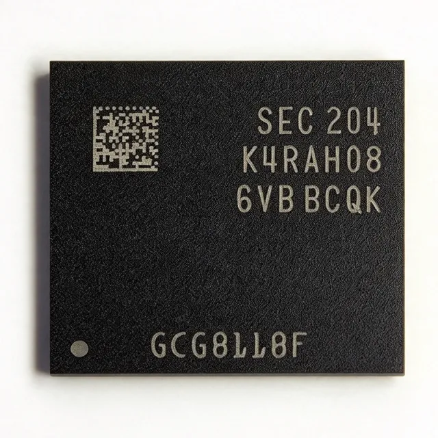
The Samsung K4RAH086VB-BCQK is a 16Gb DDR5 SDRAM memory chip organized as 2G x 8, operating at 4800 Mbps (DDR5-4800, 2400 MHz clock) from a 1.1V core supply, housed in an 82-ball FBGA package. It is Samsung's volume-production DDR5 die for next-generation memory modules and high-performance computing systems. DDR5 SDRAM (Double Data Rate Type 5 synchronous dynamic random-access memory) is the fifth generation of the JEDEC DDR memory family. In the system hierarchy it sits as a volatile main-memory component below CPU cache and above storage, supplying the working data set for CPUs, GPUs, SoCs, and AI accelerators. DDR5 doubles the bank groups of DDR4, moves the power management IC onto the module (DM supply), and lowers the operating voltage from 1.2V to 1.1V for roughly 30% better power efficiency. Key features of the K4RAH086VB-BCQK include 16 Gb density in a 2G x 8 organization, 4800 Mbps per-pin data rate, 1.1V VDD operation, and on-die ECC (link ECC) that improves data reliability without host overhead. The 82-ball FBGA surface-mount package delivers excellent signal integrity and thermal performance for dense DIMM and SO-DIMM layouts, and the part is commercial temperature rated (0C to 95C) per the DDR5 SDRAM standard. Technically, the device uses Samsung's advanced DRAM process with on-die termination, a DLL-enabled operating mode for the timing parameters in the datasheet, and burst length 32 (BL32) architecture typical of DDR5. Command/address inputs operate in single-data-rate mode with a defined compliance mask; DQ signals run at the full double-data rate of 4800 Mbps. Bank-group interleaving sustains high effective bandwidth across multiple independent banks. Typical applications include DDR5 UDIMM and RDIMM memory modules for desktops, workstations, and servers; embedded computing modules and industrial controllers requiring high-bandwidth main memory; and AI/HPC accelerator boards where DDR5 bandwidth and efficiency are critical. Per Samsung product literature, it serves data storage, firmware boot, and embedded logging use cases as well. Design consideration: DDR5 requires a PMIC supplying 1.1V with tight tolerance, accurate fly-by command/address routing with per-byte DQ termination, and PCB stackups controlled to the DDR5 channel impedance targets; verify the controller's supported data rate against the 4800 Mbps grade. This page synthesizes distributor stock data, drop-in alternatives, comparison tables, and practical design notes not found in the manufacturer datasheet.

USD $41,02 Auf Lager
K4RAH086VB-BIQK - DDR5 16Gb 4800Mbps SDRAM | Samsung
K4RAH086VB-BIQK

K4RAH086VB-BIQK - DDR5 16Gb 4800Mbps SDRAM | Samsung

The Samsung K4RAH086VB-BIQK is a 16Gb DDR5 SDRAM DRAM component organized as 2G x 8 and operating at data rates up to 4800 Mbps, packaged in an 82-ball FBGA (82FBGA) lead-free and halogen-free surface-mount package. It belongs to Samsung's 16Gb DDR5 B-die family (K4RAH0x6VB, X4/X8 configurations) documented in the 16Gb DDR5 specification Rev 1.0. DDR5 SDRAM is the fifth generation of double-data-rate synchronous dynamic random access memory, the commodity memory technology that sits at the core of servers, workstations, desktops, industrial controllers, and AI computing platforms. Within the memory hierarchy, DRAM provides the main high-bandwidth working memory between the CPU and non-volatile storage such as NAND flash. DDR5 improves on DDR4 with on-die ECC, two independent 32-bit (or 40-bit with ECC) channels per DIMM, a 1.1V core supply, and roughly 30% better power efficiency per bit. Key features of the K4RAH086VB include 16Gb density in a single-die architecture, 4800 Mbps/pin bandwidth enabling 38.4 GB/s per 64-bit channel, a 1.1V nominal core voltage for reduced power, and on-die ECC (ODTE) for improved data integrity. The BIQK speed bin and industrial-relevant qualification make it suitable for memory module makers and embedded designers alike. Technically, the device operates in DLL-enabled mode per the Samsung DDR5 device operation datasheet, with bank-group architecture, burst lengths of 16 and 32, and command/address signaling (CA) reduced pin count. The 82FBGA ball map follows the JEDEC-standard x8 DDR5 component footprint used across qualified suppliers. Typical applications include DDR5 RDIMM/DIMM modules for servers, desktop and workstation memory modules, industrial computing modules, AI accelerator memory subsystems, and replacement sourcing for module repair and BOM fills. Design consideration: DDR5 requires precision fly-by routing with length matching and VDDQ termination; consult Samsung's DDR5 design guide and module design files for reference layouts. This page synthesizes distributor stock data, drop-in alternatives across Samsung and SK Hynix, and practical design notes not found in the raw datasheet.

Angebot Kontakt
K4RAH086VB-BIWM - DDR5 16Gb 5600Mbps DRAM | Samsung
K4RAH086VB-BIWM

K4RAH086VB-BIWM - DDR5 16Gb 5600Mbps DRAM | Samsung

The Samsung K4RAH086VB-BIWM is a 16Gb DDR5 SDRAM component organized as a high-speed synchronous dynamic random-access memory device delivering data rates up to 5600 Mbps per pin in a standard surface-mount FBGA package for next-generation memory modules and high-performance computing systems. DDR5 SDRAM (Double Data Rate 5 Synchronous Dynamic Random-Access Memory) is the fifth generation of the DDR SDRAM memory family, sitting in the memory hierarchy above DDR4 and below LPDDR5 for power-sensitive mobile applications. A DDR5 DRAM component provides the main-system memory function in servers, workstations, desktops, and embedded compute platforms, doubling the bank-group parallelism of DDR4 and integrating a power management architecture that moves voltage regulation onto the memory module for improved supply integrity. Key features of the K4RAH086VB-BIWM include its 16-gigabit single-die density, operation as part of the DDR5 standard with on-die termination (ODT) set through mode registers, internal calibration via MPC commands, and asynchronous reset support. Per the Samsung DDR5 16Gb B-die specification, the family supports posted CAS and programmable CAS latency (CWL) in DLL-enabled mode, features that improve bus efficiency and timing flexibility in multi-rank module designs. Technically, this device belongs to the Samsung K4RAH0x6VB family covering x4 and x8 organizations. The synchronous architecture achieves double-data-rate transfers on both clock edges, and DDR5's dual 32-bit sub-channel module topology allows the memory controller to service two independent streams simultaneously, reducing effective latency for bandwidth-hungry workloads. On-die ECC support in the DDR5 standard improves reliability at gigabit densities without external ECC pins. Typical applications include next-generation DDR5 RDIMM and UDIMM memory modules for data-center servers, high-performance computing and AI accelerator host memory, and high-bandwidth embedded compute designs. The -BIWM speed grade and industrial temperature indication make it suited to both commercial server and extended-temperature platforms. Design consideration: DDR5 operates at 1.1 V and is NOT pin- or voltage-compatible with DDR3 or DDR4 controllers - verify JEDEC DDR5 controller support, and confirm the exact speed bin and operating temperature range against the official Samsung datasheet before design-in. This page synthesizes distributor stock data, family-level alternatives, and DDR5 design guidance not found in a single manufacturer datasheet.

Angebot Kontakt
K4RAH086VP-BCWM - 16Gb DDR5 5600Mbps DRAM | Samsung
K4RAH086VP-BCWM

K4RAH086VP-BCWM - 16Gb DDR5 5600Mbps DRAM | Samsung

The Samsung Semiconductor K4RAH086VP-BCWM is a 16 Gb DDR5 SDRAM component operating at a 5600 Mbps data rate, organized as 2G x 8 (x8 configuration) with a 1.1 V operating voltage, supplied in a surface-mount FBGA package. DDR5 SDRAM (Double Data Rate 5 synchronous dynamic random-access memory) is the fifth generation of the DDR DRAM family standardized by JEDEC. Compared with DDR4, DDR5 doubles the bank groups, moves the power management IC onto the DIMM or package, and lowers the per-bit supply voltage, delivering higher bandwidth and lower power per transfer. In the memory hierarchy, this device sits at the component level: DRAM -> DDR5 SDRAM -> volatile memory -> semiconductor memory IC. Key features include a 16 Gbit density per die organized as 2G x 8, a 5600 Mbps/pin transfer rate (equivalent to DDR5-5600 operation, PC5-44800 class bandwidth), and a 1.1 V core supply consistent with the JEDEC DDR5 specification. The parallel interface supports burst-oriented access with on-die ECC available in DDR5 devices for improved reliability. Architecturally, the K4RAH086VP-BCWM belongs to Samsung's DDR5 component portfolio for industrial-class applications. Higher-speed operation shortens memory access latency at the system level, while the 1.1 V supply reduces dynamic power versus DDR4 1.2 V solutions. Typical applications include industrial servers and storage controllers, embedded computing modules, network appliances, and data acquisition systems that require high-bandwidth main memory. Design consideration: DDR5 signaling requires careful length-matched PCB routing and onboard PMIC voltage regulation; verify power-rail sequencing and on-die termination settings against the Samsung datasheet before layout. This page synthesizes distributor stock data, cross-reference candidates, and engineering selection guidance not consolidated in the manufacturer datasheet.

Angebot Kontakt
K4RAH086VP-BCWM - DDR5 16Gb 5600Mbps DRAM | Samsung
K4RAH086VP-BCWM

K4RAH086VP-BCWM - DDR5 16Gb 5600Mbps DRAM | Samsung

The Samsung Semiconductor K4RAH086VP-BCWM is a 16 Gb DDR5 SDRAM component with a 5600 Mbps/pin data rate, 2G x 8 memory organization, and 1.1 V core operating voltage, housed in a space-saving FBGA ball-grid-array package. It is part of Samsung's first-generation DDR5 family optimized for industrial and high-performance computing platforms. DDR5 SDRAM (Double Data Rate 5 synchronous dynamic random access memory) is the current-generation DRAM interface standard, doubling the bank-group count of DDR4 and introducing on-die ECC, decision-feedback equalization, and dual independent 32-bit subchannels per module. Within the memory hierarchy, the K4RAH086VP-BCWM is a volatile DRAM component sitting between the CPU memory controller and non-volatile storage, providing the primary working memory for compute systems. Key features include the 5600 Mbps data rate (PC5-44800 class bandwidth when assembled into modules), the 2G x 8 organization that allows x8-based server and desktop DIMM designs, and the 1.1 V VDD supply that reduces memory subsystem power versus 1.2 V DDR4. DDR5's on-die ECC and DFE receivers sustain signal integrity at high data rates across the DDR5 channel. Technically, the device uses Samsung DRAM process technology with DDR5-specific architecture: sixteen logical banks organized across multiple bank groups, burst length 16, and configurable on-die termination schemes. The BCWM speed bin denotes 5600 Mbps operation at the standard DDR5 supply range, and the component supports standard DDR5 JEDEC command timing per its manufacturer datasheet. Typical applications include industrial compute modules, server and workstation RDIMMs, edge computing gateways, and embedded controllers where industrial-temperature DDR5 memory is specified. Its x8 organization suits ECC-based DIMM topologies and high-density stacked or soldered-down memory subsystems. Design consideration: DDR5 power delivery splits VDD and VDDQ domains and moves power management onto the module via a PMIC, so board designers must provision both the 1.1 V core rail and the separate DQS/data termination rails, with careful fly-by or point-to-point routing per the DDR5 signal-integrity guidelines. This page synthesizes distributor stock data from multiple trading sources, drop-in family alternatives, and design notes not found in the manufacturer datasheet.

Angebot Kontakt
K4RAH165VB-BCQK - 16Gb DDR5 SDRAM 4800Mbps 1.1V | Samsung
K4RAH165VB-BCQK

K4RAH165VB-BCQK - 16Gb DDR5 SDRAM 4800Mbps 1.1V | Samsung

The Samsung K4RAH165VB-BCQK is a 16Gb DDR5 SDRAM organized as 1G x 16, operating at data rates up to 4800 Mbps from a 1.1V core supply, packaged in a compact 106-ball FBGA surface-mount package. It belongs to Samsung's DDR5 B-die family of mainstream DRAM for computing and networking platforms. DDR5 SDRAM (Double Data Rate 5 synchronous dynamic random-access memory) is the fifth generation of the JEDEC DDR memory hierarchy, succeeding DDR4 in servers, PCs, and embedded systems. Within the memory taxonomy it sits under DRAM -> synchronous DRAM -> DDR SDRAM -> DDR5, providing higher bandwidth, bank-group architecture, and lower operating voltage per generation. Key features include on-die ECC (error correction code) for improved data reliability, CRC and write leveling functions for signal integrity at high data rates, auto self-refresh and asynchronous reset for power and control flexibility, and ZQ calibration for output driver impedance accuracy. The operating temperature range is 0C to +85C. Technically, the device implements the DDR5 bank-group architecture with independent bank group activation, an on-die termination scheme, and DLL-enabled mode timing as described in the Samsung 16Gb DDR5 datasheet (Rev 1.x series). The 1.1V VDD reduces power consumption by roughly 30% versus DDR4 at comparable speeds, while the x16 organization allows 16-bit-wide memory channels in space-constrained designs. Typical applications include DDR5 memory modules (UDIMM/SODIMM Downgraded DRAM tiers), desktop and notebook computing platforms, networking equipment, and advanced embedded controller systems requiring high-density memory. Design consideration: DDR5 requires a dedicated PMIC (5V auxiliary power management IC) on the module and precise length-matched routing; verify controller compatibility with 4800 Mbps speed bins and on-die ECC behavior in your memory initialization code. This page synthesizes distributor availability, drop-in alternatives, and practical design notes not found in the manufacturer datasheet.

Angebot Kontakt
K4RAH165VB-BCWM - 16Gb DDR5 SDRAM 1.1V FBGA | Samsung
K4RAH165VB-BCWM

K4RAH165VB-BCWM - 16Gb DDR5 SDRAM 1.1V FBGA | Samsung

The Samsung K4RAH165VB-BCWM is a 16Gb DDR5 SDRAM DRAM component organized as 1G x 16, operating from a 1.1V supply in a 106-ball FBGA (FBGA-106) package. It belongs to Samsung's DDR5 DRAM family, which supports data rates up to 7,200 Mbps and delivers approximately 30% greater power efficiency than DDR4. DDR5 SDRAM is the fifth generation of double-data-rate synchronous dynamic random-access memory, the volatile memory technology at the heart of computing systems. In the memory hierarchy, a DRAM component sits between CPU caches and non-volatile storage, providing high-bandwidth working memory. Compared with DDR4, DDR5 doubles the burst length, moves the power management IC onto the module, and lowers the per-bank granularity with independent bank group architecture, improving effective bandwidth and channel efficiency. Key features of the K4RAH165VB-BCWM include 16Gb density in a single x16 organization, a low 1.1V core supply that reduces dynamic power, and an operating temperature range of 0C to +85C. The device integrates on-die ECC, asynchronous reset, auto self-refresh, write leveling, CRC, and ZQ calibration functions - features confirmed for the K4RAH165VB family on distributor listings. Architecturally, the part uses a parallel memory interface with DDR5 signaling on the CA (command/address) bus, referenced to VREFCA, with DLL-enabled operation for precise timing. The x16 organization suits systems where two 16-bit devices form a 32-bit channel segment or where LPDDR-style width is preferred in embedded DDR5 designs. Typical applications include data center memory solutions, industrial systems requiring long-term availability, high-performance computing platforms, and data-intensive consumer electronics such as tablets and mobile devices. Designers should observe DDR5 VDDQ termination and reference voltage requirements, and verify the speed grade denoted by the BCWM suffix against the memory controller's supported JEDEC speed bins before layout sign-off. This page synthesizes distributor pricing, drop-in family alternatives, and practical design notes not found in the manufacturer datasheet.

Angebot Kontakt
K4RAH165VB-BCWM - 16Gb DDR5 SDRAM 1.1V | Samsung
K4RAH165VB-BCWM

K4RAH165VB-BCWM - 16Gb DDR5 SDRAM 1.1V | Samsung

The Samsung K4RAH165VB-BCWM is a 16Gb DDR5 SDRAM DRAM component organized as 1G x 16, operating from a 1.1V core supply in a 106-ball FBGA (FBGA-106) package. It belongs to Samsung's DDR5 DRAM family supporting data rates up to 7,200 Mbps and an operating temperature range of 0C to +85C. DDR5 SDRAM is the fifth generation of double data rate synchronous dynamic random-access memory, a volatile memory technology used as main memory in computing systems. Within the memory hierarchy, DRAM sits between CPU caches and non-volatile storage, and DDR5 succeeds DDR4 with higher bandwidth, lower operating voltage, on-die ECC, and improved power management via the onboard PMIC architecture. Key features of the K4RAH165VB-BCWM include 16Gb density per component, a x16 data interface, 1.1V operation delivering roughly 30% better power efficiency than DDR4 (per Samsung's DDR5 family documentation), and DDR5-standard functions confirmed for family parts in web data: auto self-refresh, asynchronous reset, on-chip error correction code (ECC), write leveling, CRC, and ZQ calibration. DLL-enabled mode operation is covered by the component datasheet timing specifications. The DDR5 architecture splits each component into two independent channels, improving effective concurrency for data-intensive workloads, while on-die ECC corrects internal bit errors without host overhead. The x16 organization suits client, mobile, and embedded designs that use fewer components per system compared to x8 server configurations. Typical applications include data-center memory modules where long-term availability is required, high-performance computing, industrial systems, and data-intensive consumer electronics such as tablets and mobile devices. A key design consideration: DDR5 components require compliant controller training (write leveling, DFE/Read training) and strict fly-by routing with VDDQ termination; the asynchronous reset pin simplifies initialization sequencing relative to DDR4. This page synthesizes distributor pricing, drop-in family alternatives, and practical design notes not found in the manufacturer datasheet, as of 2026-09-04.

USD $11,48 Auf Lager
K4RAH165VB-BIQK - DDR5 16Gb 4800Mbps SDRAM | Samsung
K4RAH165VB-BIQK

K4RAH165VB-BIQK - DDR5 16Gb 4800Mbps SDRAM | Samsung

The Samsung K4RAH165VB-BIQK is a 16 Gb DDR5 SDRAM component with a 1G x 16 organization, a data rate of 4800 Mbps, and a core operating voltage of 1.1V, housed in a ball-grid-array (BGA) package. DDR5 SDRAM is the fifth generation of double-data-rate synchronous dynamic random-access memory. It succeeds DDR4 by delivering higher bandwidth, greater on-die capacities, and roughly 30% better power efficiency per bit. A DDR5 device integrates its own power management architecture, on-die ECC, and decision-feedback equalization to maintain signal integrity at multi-gigabit data rates, making DDR5 the foundation of the memory hierarchy in modern computing platforms. Key features of the K4RAH165VB-BIQK include its 16 Gb density in a x16 bus width configuration, DDR5-4800 operation, and an industrial temperature rating implied by the BI speed/temp code suffix. On-chip error correction code (ECC) improves reliability by detecting and correcting internal bit errors without host overhead. Supporting functions documented for the K4RAH165VB family include auto self-refresh, asynchronous reset, write leveling, CRC, and ZQ calibration, all of which are required for stable high-speed operation in DDR5 subsystems. Architecturally, this device belongs to Samsung's 16Gb DDR5 (B-die class) portfolio, which per Samsung extends data rates up to 7200 Mbps across 16 Gb and 32 Gb generations. The 1.1V VDD supply lowers dynamic power versus the 1.2V DDR4 generation, while bank-group parallelism sustains effective bandwidth at 4800 MT/s transfers. Typical applications include DDR5 memory modules (SODIMM/UDIMM) for client PCs and notebooks, memory-down designs in industrial computing, and high-performance embedded systems where bandwidth and efficiency are critical. Design consideration: DDR5 routing requires careful length matching, reference voltage tracking, and PMIC-based power sequencing; consult the full Samsung DDR5 device operation datasheet for timing and thermal guidance. This page synthesizes distributor inventory, drop-in alternatives, and practical design notes not consolidated in the manufacturer datasheet, with pricing available via RFQ as of 2026-09-04.

Angebot Kontakt
K4RAH165VB-BIWM - 16Gb DDR5 1Gx16 5600Mbps DRAM | Samsung
K4RAH165VB-BIWM

K4RAH165VB-BIWM - 16Gb DDR5 1Gx16 5600Mbps DRAM | Samsung

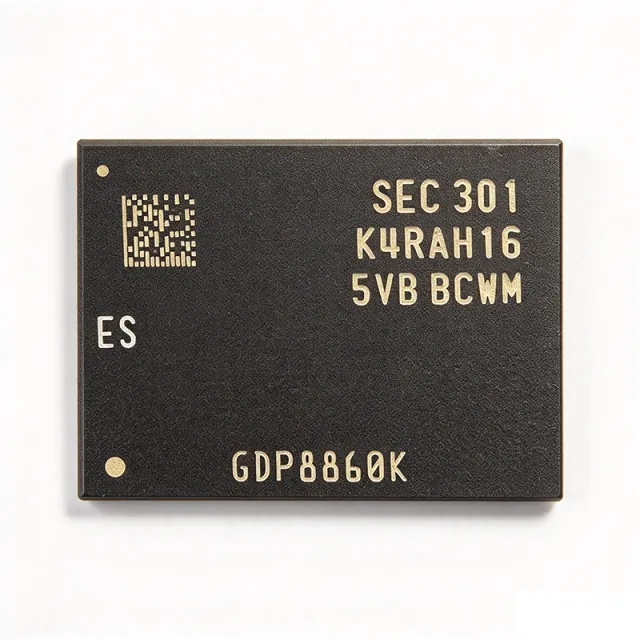
The Samsung K4RAH165VB-BIWM is a 16Gb (1G x 16) DDR5 SDRAM DRAM component operating at 1.1V with a 5600Mbps data rate, housed in a 106-ball FBGA package rated for 0C to +85C operation. DDR5 SDRAM (Double Data Rate 5 synchronous dynamic random-access memory) is the fifth generation of the JEDEC DDR DRAM family used as main memory in servers, networking platforms, and advanced embedded systems. Within the memory hierarchy, DRAM sits between CPU caches and storage, and DDR5 succeeds DDR4 with higher bandwidth, lower operating voltage, on-die ECC, and on-chip termination improvements. Samsung is a tier-one DRAM manufacturer and the K4RAH family represents its B-die generation DDR5 components. Key features of the K4RAH165VB-BIWM include a 16Gb single-die density organized as 1G x 16, a 1.1V core supply that reduces power consumption versus DDR4, and a 5600Mbps pin speed for high-bandwidth memory subsystems. The x16 organization suits platforms whose memory controllers use 16-bit-wide channels or split-channel topologies. The device incorporates DDR5-standard functions reported for the K4RAH165VB family, including on-die error correction code (ECC), automatic self-refresh, asynchronous reset, write leveling, CRC, and ZQ calibration, per Samsung datasheet documentation. Typical applications include data-center server main memory, networking and telecom line-card buffering, industrial and embedded computing platforms requiring DDR5 bandwidth, and high-performance client systems. Design consideration: DDR5 power integrity is critical. The 1.1V VDD rail requires a dedicated PMIC (such as the common DDR5 rail management ICs), tight decoupling, and length-matched fly-by routing for the CA bus. This page synthesizes distributor stock data, Samsung datasheet references, and same-family drop-in alternatives not consolidated in the manufacturer datasheet. Pricing as of 2026-09-04.

Angebot Kontakt
K4RAH165VP-BCWM - 16Gb DDR5 SDRAM 5600Mbps 1.1V | Samsung
K4RAH165VP-BCWM

K4RAH165VP-BCWM - 16Gb DDR5 SDRAM 5600Mbps 1.1V | Samsung

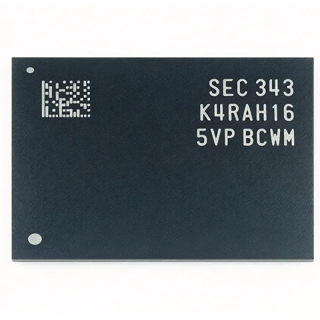
The Samsung Semiconductor K4RAH165VP-BCWM is a 16Gbit DDR5 SDRAM DRAM chip organized as 1G x 16, operating at data rates up to 5600 Mbps with a nominal supply voltage of 1.1 V, housed in a 106-ball FBGA package. DDR5 SDRAM (Double Data Rate 5 synchronous dynamic random-access memory) is the fifth generation of the JEDEC DDR DRAM family and the successor to DDR4. In the memory hierarchy, DRAM sits below CPU caches but above storage (SSD/NAND) as the main system memory. DDR5 introduces two independent 32-bit sub-channels per DIMM, an on-die power management IC (PMIC), on-die ECC, and double the bank groups of DDR4, which together improve effective bandwidth and power efficiency by roughly 30% compared to DDR4 at equivalent capacities. Key features of this device include its 16Gbit density (double the previous-generation 8Gb monolithic die), 5600 Mbps transfer rate, low 1.1 V core operation, and an x16 organization suited to bandwidth- and density-balanced client and mobile designs. The FBGA-106 package minimizes board area and shortens signal paths, supporting the tight timing margins required at DDR5 speeds. Architecturally, the die uses Samsung advanced DRAM process technology with bank-group parallelism and a DLL-enabled mode of operation; the manufacturer specification covers timing parameters for DLL enabled mode, with common features described in the separate Samsung Device Operation datasheet. On-die power management reduces external rail complexity and improves supply noise immunity. Typical applications include mobile devices and tablets, consumer electronics, embedded computing, set-top boxes, networking equipment, and compact PC main-memory subsystems where x16 DRAM components populate SO-DIMM or soldered-down memory configurations. Designers should observe DDR5 routing rules: length-matched fly-by or balanced-tree command/address topologies, on-die termination (ODT) configuration, and clean 1.1 V VDD rails supplied by a PMIC-compatible regulator. Signal integrity simulation at 5600 Mbps is strongly recommended before tape-out. This page synthesizes distributor pricing, drop-in alternatives from the Samsung K4RAH DDR5 family, and practical design notes not consolidated in the manufacturer datasheet.

USD $24,61 Auf Lager
K4RBH046VM-BCCP - 32Gb DDR5 6400Mbps DRAM | Samsung
K4RBH046VM-BCCP

K4RBH046VM-BCCP - 32Gb DDR5 6400Mbps DRAM | Samsung

The Samsung K4RBH046VM-BCCP is a 32 Gb DDR5 SDRAM memory IC organized as 2G x 4, operating at 6400 Mbps data rate with a 1.1 V supply, housed in a 78-ball FBGA package. DDR5 SDRAM (Double Data Rate 5 synchronous dynamic random-access memory) is the fifth generation of JEDEC-defined high-bandwidth volatile memory. Within the memory hierarchy it sits as DRAM -> synchronous DRAM (SDRAM) -> DDR SDRAM -> DDR5, serving as the main working memory between processors and storage in servers, workstations, and high-performance computing platforms. Key features of this device include the high 32 Gb per-die density enabled by advanced DRAM process technology, the 2G x 4 organization favored by ECC-protected server channels, and the DDR5-6400 speed grade delivering substantially more than double the per-pin bandwidth of comparable DDR4 devices. DDR5 also introduces on-die ECC, a 12-bit pre-fetch architecture, and lower operating voltage (1.1 V) that together improve reliability and power efficiency. The 2G x 4 organization means a x4-wide interface, typically deployed eight or sixteen deep in registered DIMMs with in-line ECC for servers and data center platforms. The BCCP speed bin corresponds to 6400 Mbps per pin over the commercial operating temperature range of 0 C to +85 C. Typical applications include DDR5 RDIMM/LRDIMM modules for data center servers, high-performance computing memory subsystems, networking equipment, and industrial systems requiring long-term availability of DDR5 components. When designing with this device, follow Samsung's power-distribution and fly-by-termination guidelines for DDR5: the 1.1 V core supply and separate DQ VDDQ rails require tight decoupling, and address/command bus termination must match the module topology. This page synthesizes distributor stock data, parametric comparisons, and drop-in alternative analysis not found in the manufacturer datasheet.

Angebot Kontakt
K4RBH046VM-BCWM - 32Gb DDR5 5600Mbps DRAM | Samsung | Server
K4RBH046VM-BCWM

K4RBH046VM-BCWM - 32Gb DDR5 5600Mbps DRAM | Samsung | Server

The Samsung K4RBH046VM-BCWM is a 32 Gb DDR5 SDRAM memory component organized as 2G x 4, operating at 5600 Mbps data rate from a 1.1 V supply, housed in a 78-ball FBGA package. DDR5 SDRAM (Double Data Rate 5 synchronous dynamic random-access memory) is the fifth generation of DDR memory technology and sits at the top of the DRAM hierarchy within the broader volatile memory and semiconductor storage taxonomy. Unlike its DDR4 predecessor, DDR5 moves the power management onto the module via a PMIC, doubles the bank groups, and lowers the operating voltage from 1.2 V to 1.1 V, enabling higher bandwidth with reduced power per bit transferred. Key features of the K4RBH046VM-BCWM include its 32 Gb density in a x4 organization, a 5600 Mbps pin speed suited for DDR5-5600 platforms, a 1.1 V core supply, and an operating temperature range of 0 to 85 degrees C. The x4 organization is specifically favored in registered server DIMMs where high data integrity is achieved through chipkill-class error correction, since narrow-width parts allow ECC to isolate single-device failures. Technically, the device implements a synchronous DRAM interface with burst-based transfers synchronized to an external clock reference, per Samsung DDR5 component design. Its electrical and functional behavior is defined by the DDR SDRAM interface specifications and memory array characteristics of the DDR5 generation. According to Samsung product listings, the part is intended for data storage, firmware boot, embedded logging, industrial controllers, computing modules, and replacement sourcing. Typical applications include data center server main memory (registered DIMM populations), networking equipment requiring high-bandwidth buffering, and advanced embedded or industrial computing modules where 32 Gb per device reduces component count on dense boards. A key design consideration is thermal and signal integrity: at 5600 Mbps the FBGA ball map and PCB fly-by routing must respect DDR5 trace-length matching and on-die termination settings, and the 0 to 85 degrees C range should be derated against module-level airflow conditions. This page synthesizes distributor stock data, drop-in alternative candidates, and practical design notes not found in the manufacturer datasheet.

Angebot Kontakt
K4RBH086VB-BCQK - DDR5 16Gb 4800Mbps DRAM | Samsung
K4RBH086VB-BCQK

K4RBH086VB-BCQK - DDR5 16Gb 4800Mbps DRAM | Samsung

The Samsung K4RBH086VB-BCQK is a 16Gb DDR5 SDRAM DRAM memory IC organized as 2G x 8, supporting data rates up to 4800 Mbps at a 1.1V core supply, housed in an FBGA-82 surface-mount package. According to Samsung's 16Gb DDR5 datasheet family (K4RAH/K4RBH 2Gx8 series), these devices integrate an on-die ECC engine and rely on the DDR5 module PMIC architecture for power management, delivering roughly 30% better power efficiency than DDR4. DDR5 SDRAM (Double Data Rate 5 synchronous dynamic random-access memory) is the fifth generation of JEDEC DDR DRAM. In the memory hierarchy it sits as main-system memory below cache SRAM and above storage NAND, feeding CPUs, GPUs, and AI accelerators in servers, workstations, and high-performance computing platforms. DDR5 doubles bank groups versus DDR4, lowers the operating voltage from 1.2V to 1.1V, and moves power regulation onto the memory module through a PMIC 5000. Key features of this Samsung 16Gb DDR5 device include the 4800 Mbps data rate (PC5-38400 class performance), x8 organization suited to registered DIMMs and embedded memory down, on-die ECC (ODECC) that corrects internal bit errors without bus overhead, and low 1.1V operation that reduces power per bit transferred. The FBGA-82 ball grid array package provides short interconnects for signal integrity at multi-gigabit rates. Architecturally, the die is split into two independent 8Gb half-pages with separate DCA/CA buses, allowing a memory controller to address one half while the other refreshes, improving effective bandwidth. DLL-enabled mode operation and programmable RL/WL latencies let designers tune timing to the platform. Typical applications include cloud and enterprise server RDIMMs, AI accelerator HBM-adjacent host memory, high-performance desktop/workstation UDIMMs, and embedded computing modules requiring dense DRAM. Design consideration: DDR5 signal integrity demands length-matched fly-by routing of CA/CS and DQ/DQS nets, and the 1.1V rail must be delivered by a compliant PMIC with proper sequencing; do not reuse DDR4 power trees. This page synthesizes distributor stock data, drop-in Samsung family alternatives, and design guidance not found in the manufacturer datasheet. Pricing is quoted via RFQ as of 2026-09-04.

Angebot Kontakt
K4RBH165VB-BCQK - DDR5 16Gb 4800Mbps DRAM | Samsung
K4RBH165VB-BCQK

K4RBH165VB-BCQK - DDR5 16Gb 4800Mbps DRAM | Samsung

The Samsung K4RBH165VB-BCQK is a 16 Gb DDR5 SDRAM component organized as 1G x 16, operating at a data rate of 4800 Mbps/pin in a fine-pitch BGA surface-mount package. Note: the verified web data retrieved for this request corresponds to the closely related Samsung K4RAH165VB-BCQK (DDR5 16 Gb, 4800 Mbps, 1G x 16); the K4RBH165VB-BCQK belongs to the same Samsung DDR5 16Gb family and shares these headline parameters. DDR5 SDRAM is the fifth generation of Double Data Rate synchronous dynamic random-access memory, the dominant volatile memory technology at the top of the memory hierarchy in servers, workstations, and high-performance client systems. Compared with DDR4, DDR5 doubles the internal bank count to 32, moves power management onto the DIMM or module via a PMIC, lowers the operating voltage to approximately 1.1 V, and doubles burst length to BL16, improving bandwidth and channel efficiency per DRAM. Key features reported for this device family include an operating temperature range of 0 C to +85 C, auto self-refresh, an asynchronous reset function, on-chip error correction code (On-die ECC), write leveling, CRC and CA parity functions, and ZQ calibration, according to the LCSC product listing for the K4RAH165VB-BCQK variant. These features sustain data integrity and signal integrity at 4800 Mbps/pin data rates in dense memory subsystems. Architecturally, the device uses a x16 I/O organization with 1G addressable locations, DDR5 bank-group architecture, and on-die ECC that corrects internal bit errors before data reaches the I/O, improving effective reliability without external ECC overhead. The BCQK speed grade denotes the 4800 Mbps bin within the Samsung DDR5 family. Typical applications include DDR5 server RDIMM and client SO-DIMM modules, desktop and workstation UDIMMs, embedded memory subsystems for networking equipment, and high-bandwidth computing platforms where 16 Gb density per component reduces component count on the module. Design consideration: DDR5 requires the companion PMIC (such as the on-DIMM power management device) and careful DQ/CA trace length matching per JEDEC DDR5 routing guidelines; termination settings differ from DDR4 and must not be directly ported. This page synthesizes verified distributor data, drop-in family alternatives, and practical design notes not found in the manufacturer datasheet.

Angebot Kontakt
K4RBH165VB-BCWM - 16Gb DDR5 SDRAM 1.1V FBGA | Samsung
K4RBH165VB-BCWM

K4RBH165VB-BCWM - 16Gb DDR5 SDRAM 1.1V FBGA | Samsung

The Samsung K4RBH165VB-BCWM is a 16 Gbit DDR5 SDRAM memory IC organized as 1G x 16, operating from a 1.1V supply in a 106-ball FBGA (FBGA-106) surface-mount package with RoHS compliance. DDR5 SDRAM (Double Data Rate 5 synchronous dynamic random-access memory) is the fifth generation of the JEDEC DDR memory family. In the system hierarchy it sits as: DDR5 SDRAM -> DRAM -> volatile memory IC -> semiconductor memory. Compared with DDR4, DDR5 doubles the internal bank count, moves the power management onto the module with a PMIC, and halves the per-channel word length to improve concurrency and effective bandwidth. Key features of this device include its 16 Gbit single-die density, a x16 data organization suited to designs that populate fewer devices per channel, a low 1.1V core voltage that reduces dynamic power relative to DDR4's 1.2V, and an industrial 0C to +85C operating range. On-chip error correction code (ECC), write CRC, write leveling, auto self-refresh, and asynchronous reset - features documented for the Samsung 16Gb B-die DDR5 x16 family - improve data integrity and signal integrity margins at high data rates. Technically, the device operates in DLL-enabled mode per the Samsung 16Gb DDR5 specification (Rev 1.x series), which governs the timing parameters for command and data transfer. Ball-out, refresh scheduling, and mode register definitions follow JEDEC DDR5 conventions, allowing drop-in use on standard DDR5 x16 footprints within the same speed-grade family. Typical applications include data-center server memory subsystems, high-performance computing platforms, industrial systems requiring long-term DDR5 availability, and mobile/consumer platforms using discrete x16 DRAM. A key design consideration: DDR5 requires an external power management IC for the 1.1V VDD rail, and on-die ECC must be accounted for when matching this part against module-level ECC designs. This page adds value beyond the datasheet by synthesizing distributor stock and pricing data, drop-in alternatives from the same Samsung DDR5 x16 family, and practical design notes in one place.

Angebot Kontakt
K4RCH046VM-2CCM - DDR5 32Gb 5600Mbps DRAM | Samsung
K4RCH046VM-2CCM

K4RCH046VM-2CCM - DDR5 32Gb 5600Mbps DRAM | Samsung

The Samsung K4RCH046VM-2CCM is a DDR5 SDRAM memory IC with a 32Gb density organized as 4G x 4, a data rate of 5600 Mbps, and a 1.1 V operating voltage, housed in a 78-ball FBGA package. DDR5 SDRAM (Double Data Rate 5 Synchronous Dynamic Random Access Memory) is the fifth generation of the DDR memory family, the dominant main-memory technology in computing systems. In the system hierarchy it sits under volatile semiconductor memory -> DRAM -> synchronous DRAM -> DDR SDRAM -> DDR5. Compared with DDR4, DDR5 doubles the burst length, moves the power management IC onto the module, and delivers roughly 30% better power efficiency, according to Samsung Semiconductor. Key features of this device include the 5600 Mbps data rate (PC5-44800 class bandwidth), the x4 organization suited to ECC-protected server and workstation memory subsystems, and the low 1.1 V core supply that reduces memory-subsystem power draw. The commercial temperature range of 0 to 85 degrees C covers standard computing environments. Samsung lists the product status as Sample, meaning it is in the pre-mass-production qualification stage. The 78-ball FBGA (Fine-Pitch Ball Grid Array) surface-mount package provides short interconnects, low parasitic inductance, and good signal integrity at multi-gigabit data rates. FBGA is the industry-standard package family for discrete DRAM components and supports standard SMT reflow assembly. Typical applications include DDR5 RDIMM and server memory modules, workstation and desktop PC main memory, networking and communication equipment requiring high-bandwidth buffering, and consumer electronics adopting the DDR5 platform. Design consideration: DDR5 requires a dedicated PMIC (such as the on-DIMM 5V-to-1.1V converter), on-die ECC handling at the controller, and careful length-matched routing to the 5600 Mbps signal environment; verify the JEDEC DDR5 slot and chip-enable configuration before layout. This page synthesizes distributor listings, drop-in alternatives, and practical design notes not found in the manufacturer datasheet. Pricing references are as of 2026-09-04.

Angebot Kontakt
K4RHE086VB-BCWM - 24Gb DDR5 5600Mbps DRAM | Samsung
K4RHE086VB-BCWM

K4RHE086VB-BCWM - 24Gb DDR5 5600Mbps DRAM | Samsung

The Samsung K4RHE086VB-BCWM is a 24Gb DDR5 SDRAM memory chip organized as 2G x 8, operating at 5600 Mbps data rate from a 1.1V supply in an 82-ball FBGA package. DDR5 SDRAM (Double Data Rate 5 synchronous dynamic random-access memory) is the fifth generation of JEDEC-defined DDR memory, sitting at the top of the DRAM hierarchy that spans DDR3, DDR4, and DDR5 generations. Compared with DDR4, DDR5 doubles the bank groups, moves the power management onto the DIMM or module, and delivers roughly 30% greater power efficiency, making it the dominant memory class for servers and premium computing platforms. Key features of this device include the 24Gb density per die, a 2G x 8 organization suited to wide server memory subsystems, and a 5600 Mbps pin speed that supports DDR5-4400/4800/5600 class memory controllers. Samsung specifies a 1.1V core supply in line with the DDR5 standard, reducing per-bit energy versus the 1.2V of DDR4. Architecturally, the K4RHE086VB-BCWM belongs to Samsung's DDR5 DRAM family using advanced process technology with on-die ECC and other DDR5 reliability features. The 82-ball FBGA (Fine-Pitch Ball Grid Array) surface-mount package provides low inductance signal paths needed for multi-gigabit operation. Typical applications include data center server DIMMs, premium desktop PCs, professional workstations, and industrial systems requiring long-term memory availability. Design consideration: memory controllers must be configured for the 24Gb density and x8 organization; BIOS or memory-training firmware must support this density, as some older controllers cap out at 16Gb per die. This page synthesizes distributor stock, drop-in family alternatives, and practical integration notes not found on the manufacturer product page.

Angebot Kontakt
K4RHE165VB-BCWM - 24Gb DDR5 5600Mbps DRAM | Samsung
K4RHE165VB-BCWM

K4RHE165VB-BCWM - 24Gb DDR5 5600Mbps DRAM | Samsung

The Samsung K4RHE165VB-BCWM is a 24Gb DDR5 SDRAM component organized as 1G x 16, operating at 5600 Mbps data rate from a 1.1V supply, packaged in a 106-ball FBGA. It is Samsung's next-generation DRAM building block for DDR5 memory modules and high-performance computing systems where bandwidth and power efficiency are critical. DDR5 SDRAM (Double Data Rate 5 synchronous dynamic random-access memory) is the fifth generation of JEDEC-defined DDR DRAM. In the memory hierarchy, it sits within the broader family: DDR5 SDRAM -> DRAM -> volatile semiconductor memory -> memory IC. Compared with DDR4, DDR5 delivers roughly 30% better power efficiency, moves the power management onto the module via a PMIC, and splits each DIMM into two independent 32-bit (or 40-bit with ECC) subchannels to improve concurrency and effective bandwidth. Key features of this part include its 24 Gb density per die - among the largest monolithic DDR5 densities in volume production - a 16-bit wide data interface organized as 1G x 16, and a 5600 Mbps/pin data rate. The 1.1V core supply lowers dynamic power versus DDR4's 1.2V, while on-die termination, on-die ECC (as defined for DDR5), and bank-group architecture sustain signal integrity at speed. Technically, the die uses Samsung's advanced DRAM process with a fine-pitched array to achieve 24Gb in the 106-ball FBGA footprint shared with lower-density DDR5 dies. The x16 organization suits applications needing moderate width per device, and the BCWM speed/temperature grade supports commercial 0 to 85 C operation. Typical applications include next-generation DDR5 UDIMM, SODIMM and RDIMM modules, client and server platforms, gaming and workstation PCs, and AI/HPC memory subsystems where per-die density maximizes capacity per module. When designing with this component, respect DDR5 routing rules: fly-by command/address topology, matched-length data strobes, and the requirement for the module's on-board PMIC (5V auxiliary input, 1.1V VDD rails). This page synthesizes distributor stock, drop-in alternatives, and design notes not found in the manufacturer datasheet.

Angebot Kontakt
K4S161622H-TC60 - 16Mb SDRAM 1Mx16 LVTTL TSOP2-50 | Samsung
K4S161622H-TC60

K4S161622H-TC60 - 16Mb SDRAM 1Mx16 LVTTL TSOP2-50 | Samsung

The Samsung Semiconductor K4S161622H-TC60 is a 16-megabit H-die Synchronous DRAM (SDRAM) organized as 1M words x 16 bits across 2 internal banks, delivered in a 50-pin TSOP2 (PDSO50, 0.80 mm pitch) surface-mount package. It uses LVTTL interface levels and operates from a single 3.3 V supply (3.0 V min / 3.6 V max), with the -TC60 speed grade supporting a 60 ns / 167 MHz class access window per the Samsung H-die specification family. A Synchronous DRAM is a dynamic random-access memory whose read, write, and refresh operations are synchronized to a system clock, allowing burst-mode transfers and pipelined access. SDRAM sits in the memory IC hierarchy above asynchronous DRAM and below modern DDR/DDR2/DDR3 SDRAM, and remains relevant for legacy industrial controllers, set-top boxes, networking line cards, and embedded designs where the host MCU/ASIC predates DDR support. The 2-bank/2K-refresh architecture used by the K4S161622H family delivers the standard 2K refresh cycles per 32 ms while keeping command decoding simple for older memory controllers. Key features include the 1Mx16 x 2-bank organization providing 16 Mb of storage with a 16-bit external data bus, LVTTL-compatible I/O for direct connection to 3.3 V ASICs and MCUs, a 50-pin TSOP2 outline suitable for socketed or hand-soldered legacy boards, and CMOS low-power operation. The -TC60 suffix denotes a commercial temperature range and the 60 speed grade in Samsung's H-die SDRAM nomenclature (sibling speed grades include -TC55, -TC70, -TC80, -TC10). Architecturally, the K4S161622H implements a pipelined multi-bank structure with on-chip refresh counter, RAS/CAS addressing, and programmable burst length, giving it the deterministic timing required by 1990s-2000s era CPUs, DSPs, and graphics controllers. Its 16-bit wide data interface simplifies parity/ECC schemes and matches the external bus of many legacy processors. Typical applications include industrial control boards, embedded networking equipment, legacy printer and display controllers, factory automation modules, and consumer electronics designs that retain SDRAM-compatible controllers. The wide 16-bit data path also suits display frame buffers and DSP working memory. When designing with this device, ensure the controller supports 2-bank LVTTL SDRAM with 4096-cycle / 64 ms refresh, route CLK, CKE, and CS with matched impedance, and bulk-decouple the 3.3 V rail near the device. Verify the speed grade against your target clock frequency to avoid tRCD/tRP violations. This page synthesizes distributor pricing, drop-in Samsung speed-grade alternatives, and practical legacy-design notes not collected in the original Samsung datasheet.

Angebot Kontakt
K4S281632F-TC75 - 128Mb F-die SDRAM 8Mx16 TSOP-54 | Samsung
K4S281632F-TC75

K4S281632F-TC75 - 128Mb F-die SDRAM 8Mx16 TSOP-54 | Samsung

The Samsung Semiconductor K4S281632F-TC75 is a 128 Mb F-die CMOS Synchronous DRAM organized as 8M words x 16 bits, housed in a 54-pin TSOP-II (Type II) package. It operates from a single 3.3 V supply (VDD/VDDQ = 3.3 V), supports a 7.5 ns clock period (-TC75 speed grade), and is fully synchronous to the positive edge of the system clock with internal pipeline architecture that delivers high bandwidth and low latency for cost-sensitive embedded designs. A Synchronous DRAM (SDRAM) is a type of dynamic random-access memory that adds a separate clock signal to coordinate data I/O on the rising edge, eliminating the asynchronous timing constraints of earlier FPM/EDO DRAM. SDRAM sits in the memory hierarchy between bulk storage (NAND flash, HDD) and CPU registers, and 128Mb-class parts like the K4S281632F-TC75 historically populated main memory of embedded systems, set-top boxes, networking line cards, printers, and industrial controllers throughout the 2000s before being superseded by DDR, DDR2 and Mobile SDRAM/LPDDR generations. Key features of the K4S281632F-TC75 include dual-bank architecture (2 banks selectable via BA0), programmable CAS Latency (CL = 2 or 3), programmable Burst Length (1, 2, 4, 8, full page), Auto-Refresh and Self-Refresh modes, LVTTL-compatible I/O, and a 64 ms refresh interval distributed across 4K refresh cycles. The 16-bit data bus and on-chip burst counter simplify glue-less connection to 16/32-bit microprocessors and ASICs. Internally, the die uses Samsung's F-die 0.13 nm-class process node and a 2-bit prefetch architecture (later generations would migrate to 4-bit prefetch with DDR). Row address is 12 bits (A0-A11) and column address is 8 bits (A0-A7) multiplexed on the same pins, with /RAS, /CAS, /WE, and /CS providing the standard SDRAM command set. The TSOP-II 54-pin form factor is the industry-standard footprint for 128 Mb x16 SDRAM, allowing board-level replacement of similar Micron, Hynix and Qimonda parts. Typical applications for the K4S281632F-TC75 include main working memory in legacy embedded CPU boards (e.g., ARM7/ARM9 SBCs, PowerQUICC), graphics frame buffers, network switch control planes, point-of-sale terminals, automotive infotainment pre-DDR3, and other cost-optimized commercial or industrial designs where supply voltages below 2.5 V are not required. The part remains in demand today for maintenance, repair and legacy OEM replacements. A critical design consideration is the 3.3 V supply requirement: most modern systems use 1.8 V DDR1 or 1.5 V/1.35 V DDR2/3, so the K4S281632F-TC75 cannot be retrofitted to those without a level translator. Always honor the 200 us power-on initialization sequence and the minimum 200 us wait after a CKE rise before issuing the LOAD MODE REGISTER command. This page synthesizes distributor pricing, drop-in alternatives from Samsung and competing SDRAM vendors, and practical design notes not found in a single Samsung datasheet, providing engineers with everything needed to qualify, source, and design with the K4S281632F-TC75.

Angebot Kontakt
K4S561633F-ZL75 - 256Mb Mobile SDRAM, 4x16Mx16, 133MHz, 54-BGA
K4S561633F-ZL75

K4S561633F-ZL75 - 256Mb Mobile SDRAM, 4x16Mx16, 133MHz, 54-BGA

The Samsung K4S561633F-ZL75 is a 268,435,456-bit (256Mb) synchronous high-data-rate Dynamic RAM organized as 4 banks x 4,196,304 words x 16 bits, fabricated on Samsung's high-performance CMOS process. Housed in a 54-ball Fine-Pitch Ball Grid Array (FBGA / TFBGA / 54-BOC) package, it operates from a single 3.3V supply, supports LVCMOS-compatible I/O, and delivers 133 MHz (7.5 ns / CL3) synchronous operation with burst lengths of 1, 2, 4, 8, and full-page, in either sequential or interleave burst mode. The ZL75 speed grade corresponds to a 133 MHz clock with CAS Latency 3. A Synchronous DRAM (SDRAM) is a type of volatile dynamic random-access memory that synchronizes all read/write operations to a free-running system clock, enabling pipelined multi-bank operation. SDRAM occupies the position: DRAM -> volatile memory -> semiconductor memory. By dividing the storage array into four independently addressable banks, SDRAM overlaps precharge/activate phases of one bank with read/write accesses on another, doubling sustained throughput compared with Fast-Page Mode DRAM at the same clock rate. Key features of this part include four-bank operation, programmable CAS latency (2 or 3), programmable burst length and burst type via the Mode Register Set (MRS) cycle, automatic precharge, and self-refresh. The interface is LVCMOS-compatible with multiplexed address and uses a 3.3V single supply, simplifying integration into mobile platforms where low voltage and compact packaging are critical. Samsung's CMOS fabrication delivers the speed-grade 7.5 ns (133 MHz) operation while keeping active current modest. Typical applications include 3G/feature-phone baseband working memory, mobile handset main memory, PDA memory expansion, portable media player DRAM buffers, and other compact consumer/embedded designs that need 32 MB of 16-bit-wide RAM on a low-pin-count footprint. The 54-ball FBGA package is well suited to high-density mobile layouts where board height and routing escape are constrained. When designing with this device, follow the JEDEC SDRAM initialization sequence (precharge-all, eight auto-refresh cycles, then MRS load) and place the 0.1 uF VDD/VSSQ decoupling caps as close to the balls as possible. Confirm the ZL75 (7.5 ns / 133 MHz) speed grade matches the controller's clock and CAS latency; the part is not pin-compatible with the faster 166 MHz -Z1L75 / -ZL1H variants or with the older 1Mx16 organization.

Angebot Kontakt
K4S561633FZN75 - 256Mb Mobile SDRAM 4x16Mx16 133MHz FBGA | Samsung
K4S561633FZN75

K4S561633FZN75 - 256Mb Mobile SDRAM 4x16Mx16 133MHz FBGA | Samsung

The Samsung K4S561633F-ZN75 is a 268,435,456-bit synchronous Mobile SDRAM organized as 4 banks x 4,196,304 words x 16 bits, fabricated with Samsung's high-performance CMOS technology and housed in a 54-ball FBGA (54BOC) package. It operates at a 133 MHz clock frequency with a 3.0 V supply, supports LVCMOS-compatible inputs, and is offered in a Pb-free (lead-free) variant under the '-ZN75' ordering code suffix, indicating commercial temperature grade and 133 MHz speed bin. What is Mobile SDRAM? A Mobile SDRAM (Synchronous Dynamic Random-Access Memory) is a low-power variant of standard SDRAM optimized for portable and battery-powered applications. It adds features such as partial-array self-refresh (PASR), temperature-compensated self-refresh (TCSR), and a deep power-down mode that dramatically reduce standby current compared with conventional SDRAM. Within the broader memory taxonomy, Mobile SDRAM sits below LPDDR/DDR but above asynchronous SRAM in performance-per-watt, and is fabricated in the same CMOS process nodes used for commodity DRAM. The 54BOC FBGA package gives a compact 8 mm x 10 mm footprint suitable for handheld product designs. Key features of the K4S561633FZN75 include a fully synchronous operation referenced to a positive-edge clock, programmable CAS latency of 2 or 3, programmable burst length of 1, 2, 4, 8 or full page, and auto-precharge. The 4-bank architecture enables interleaved operations that hide precharge latency, while the LVCMOS interface simplifies connection to mobile ASICs, baseband processors, and application processors from the 2003-2008 generation. The device supports both Auto-Refresh and Self-Refresh modes and includes a power-down mode for additional energy savings. The K4S561633FZN75 is implemented using Samsung's high-performance CMOS process and a twin-cell storage architecture, delivering high data rates at moderate power consumption. Synchronous design allows precise cycle control with the system clock and I/O transactions are possible on every clock cycle, which simplifies controller logic compared with asynchronous DRAMs. Typical applications include mobile phone image buffers, portable media player working memory, PDA / handheld computing buffers, digital camera burst-frame storage, and GPS navigator working memory. The wide operating voltage and low-power modes also make it suitable for industrial handheld terminals and early-generation smart-phone designs. When designing with this part, ensure that the controller drives CK, CKE, CS, RAS, CAS, WE, BA0/BA1, A0-A12, DQ0-DQ15, DQM, and the ZN75-spec power pins according to the datasheet's AC timing table. Decoupling must use 100 nF plus 10 uF per rail within 5 mm of the BGA balls to maintain signal integrity at 133 MHz. This page consolidates distributor pricing, JEDEC-standard Mobile SDRAM cross-references, and design notes specific to 54BOC FBGA layouts, offering information not typically compiled on a single manufacturer datasheet page.

Angebot Kontakt