Produkte (39.000+)

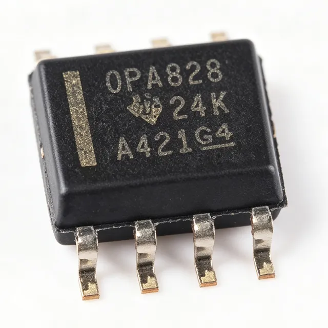
OPA828IDR - 45MHz JFET Op Amp, 4nV/√Hz | TI | Precision Amplifier
OPA828IDR

OPA828IDR - 45MHz JFET Op Amp, 4nV/√Hz | TI | Precision Amplifier

The Texas Instruments OPA828IDR is a high-speed, JFET-input operational amplifier delivering 45 MHz gain bandwidth, 150 V/us slew rate, and 4 nV/√Hz voltage noise in an 8-pin SOIC package. It operates over a wide supply range of ±4 V to ±18 V (36 V total) with rail-to-rail output (RRO), positioning it as the next-generation successor to the legendary OPA627 and OPA827 op amps. A JFET-input operational amplifier is a type of precision amplifier whose input stage uses junction field-effect transistors, providing extremely low input bias current (picoampere range) and high input impedance. Within the signal-chain hierarchy, op amps sit between sensors and data converters, serving as the general-purpose analog building block for amplification, filtering, buffering, and transimpedance conversion. Key features include 50 uV input offset voltage, 0.45 uV/C offset drift, 1 pA typical input bias current, and only 60 nVRMS of noise from 0.1 Hz to 10 Hz. These DC precision specifications make the OPA828 suitable for applications where both speed and accuracy are demanded simultaneously - a rare combination. MUX-friendly inputs allow multiplexed signal chains without settling artifacts or charge-injection damage. Architecturally, the OPA828 pairs a JFET input stage with a rail-to-rail output stage, combining classic precision topology with modern output swing. The RRO output maximizes dynamic range in low-voltage systems while the 36 V supply rating supports traditional ±15 V industrial analog rails without redesign. Typical applications include photodiode transimpedance amplifiers (TIA), high-fidelity audio front ends, precision ADC and DAC buffer stages, and active filters in test and measurement instrumentation. The wide 36 V supply range is particularly valuable for industrial designs retaining legacy ±15 V rails. For design, ensure supply decoupling with 0.1 uF ceramic capacitors placed within 3 mm of each supply pin. When replacing an OPA627, verify compensation and bias-current paths, as community feedback shows some legacy TIA circuits require adjustment despite pin compatibility. This page synthesizes distributor pricing, drop-in alternatives, and practical design notes not found in the manufacturer datasheet.

USD $1,75 Kontakt
OPA843ID - 800 MHz Wideband Operational Amplifier | Texas Instruments
OPA843ID

OPA843ID - 800 MHz Wideband Operational Amplifier | Texas Instruments

The Texas Instruments OPA843ID is a single-circuit, wideband, low-distortion, medium-gain voltage-feedback operational amplifier with an 800 MHz gain-bandwidth product, 1000 V/us slew rate, and operation from a 10 V to 12 V supply in an 8-pin SOIC package. Designed for high-speed signal chains, it combines broad bandwidth with low distortion and is suitable for communications, test-and-measurement, video, and data-acquisition systems. A voltage-feedback operational amplifier is a feedback-controlled amplifier that uses the error at its inverting input to correct the output. The OPA843 belongs to the broader operational-amplifier hierarchy, which includes instrumentation amplifiers, buffer amplifiers, comparators, and other analog signal-conditioning ICs. Its medium closed-loop gain range and wide operating bandwidth make it particularly useful when a design needs accurate high-frequency amplification rather than only low-frequency precision. The primary performance characteristics include an 800 MHz gain-bandwidth product and a 1000 V/us slew rate. These figures allow the amplifier to preserve large-amplitude signals encountered in instrumentation and RF-adjacent signal chains. The device operates from 10 V to 12 V, giving designers sufficient headroom for wide-swing output stages while supporting a dual-supply implementation centered at zero volts. The specified operating-temperature range extends from -40 °C to +85 °C for industrial-temperature applications. OPA843ID is configured as a voltage-feedback amplifier rather than a current-feedback amplifier. This topology supports conventional resistive feedback networks and is familiar to engineers designing gain blocks, active filters, impedance drivers, and signal conditioners. Because the package is an 8-pin SOIC, PCB footprint reuse is straightforward when a new amplifier has the same supply arrangement, pin functions, and feedback topology. Pin assignments and support-network details should nevertheless be checked against the manufacturer datasheet before production release. Typical applications include broadband instrumentation, communications receivers, analog-to-digital converter input interfaces, active filters, pulse-shape circuits, and test equipment. In these applications, the 800 MHz bandwidth handles fast transitions while the 1000 V/us slew rate limits slew-related distortion. When driving cables, analog-to-digital converters, or other finite-impedance loads, the output-current capability and output-voltage swing should be checked against the actual load and supply conditions. The main design trade-off is supply and output-stage headroom. A 10 V to 12 V supply supports high output swing, but it is not interchangeable with a modern low-voltage, rail-to-rail amplifier. Decoupling capacitors, feedback resistor selection, source and load impedances, and stability conditions determine practical bandwidth. Use the manufacturer datasheet and its evaluated application circuits to select compensation and confirm performance across the required gain and frequency range. This page combines the verified manufacturer and distributor product information with engineering-focused comparisons, application guidance, package details, and design notes. It highlights where the OPA843ID's bandwidth, slew rate, supply range, and low-distortion voltage-feedback architecture are most useful, while also identifying the information that must be checked in the datasheet before a drop-in PCB or production design is approved.

Angebot Kontakt
OPA858QIDSGRQ1 - 5.5GHz FET-Input TIA Op-Amp Q1 | TI
OPA858QIDSGRQ1

OPA858QIDSGRQ1 - 5.5GHz FET-Input TIA Op-Amp Q1 | TI

The Texas Instruments OPA858QIDSGRQ1 is an automotive-qualified (AEC-Q100), wideband, low-noise decompensated operational amplifier with FET (CMOS) inputs, delivering a 5.5-GHz gain bandwidth product (GBWP) while remaining stable at a minimum gain of 7 V/V. It is supplied in a compact 8-pin WSON (2x2 mm) surface-mount package. A decompensated amplifier is an operational amplifier internally compensated for stable operation only above a minimum closed-loop gain (here 7 V/V). By removing the compensation for unity-gain stability, the decompensated topology achieves dramatically higher bandwidth and lower input-referred noise than unity-gain-stable amplifiers of comparable process technology. In the signal-chain hierarchy, the OPA858-Q1 sits as a wideband voltage-feedback amplifier serving transimpedance amplifier (TIA) and high-gain voltage amplifier roles in high-speed analog front ends. Key features include the 5.5-GHz GBWP that enables high closed-loop bandwidths at transimpedance gains in the range of tens to hundreds of kilo-ohms, FET inputs that minimize input bias current effects on photodiode and high-impedance nodes, and single-ended single-channel configuration optimized for high-speed signal paths. The Q1 variant is manufactured on TI automotive flows and is qualified per AEC-Q100, supporting automotive lidar, imaging, and test applications that demand supply-chain traceability and automotive-grade reliability. The architecture combines CMOS input devices with wideband voltage-feedback internals, yielding low input capacitance that is critical in TIA designs because photodiode plus amplifier input capacitance directly limits achievable bandwidth per unit of transimpedance gain. TI provides the OPA858 together with a companion evaluation module and application collateral covering feedback resistor selection, compensation capacitor sizing, and stability analysis. Typical applications include automotive lidar receiver TIAs, wideband photodiode amplification in optical sensing, high-speed voltage amplification stages, and wideband test and measurement front ends. The device suits any signal chain that requires gain of 7 V/V or higher with multi-hundred-megahertz to gigahertz-class bandwidth. Design consideration: because the amplifier is only stable at gain >= 7 V/V, noise-gain analysis must be performed at all frequencies, including input capacitance effects at the inverting node; verify phase margin with the TI datasheet stability curves before finalizing feedback-network values.

Angebot Kontakt
OPA875ID - 700 MHz 2:1 Video Multiplexer | Texas Instruments
OPA875ID

OPA875ID - 700 MHz 2:1 Video Multiplexer | Texas Instruments

The Texas Instruments OPA875ID is a single-channel, 700 MHz video multiplexer with an integrated +2 gain amplifier, supplied in an 8-pin SOIC package. It combines two high-speed video inputs with one output, consumes only 11 mA, and provides greater than 425 MHz large-signal bandwidth with a 4 VPP signal. The OPA875ID is therefore suited to wideband video routing where compactness, low power consumption, and short signal paths are important. A high-speed video multiplexer is a signal-routing device that selects one of multiple analog inputs and presents that selected signal at a common output. The OPA875ID belongs to the broader video-switch IC and high-speed analog multiplexer categories. Unlike a general-purpose analog switch that merely connects a source to a load, it integrates a +2 video-amplifier channel and optimized input switching, allowing it to drive downstream video equipment while preserving wideband signal integrity. Principal features include a 700 MHz device bandwidth, greater than 425 MHz large-signal bandwidth at 4 VPP, +2 gain, and a single-channel 2:1 configuration. Its 11 mA supply-current consumption reduces the power burden in distributed video systems. The manufacturer's product information also indicates improved gain accuracy and switching glitch compared with earlier multiplexer solutions, using a new input-stage switching approach. The OPA875ID is available in SO-8 and small MSOP-8 package options, with OPA875ID identifying the SO-8 ordering variant. The manufacturer describes the OPA875 as a very wideband multiplexer suitable for high-speed video systems. Its architecture is intended to minimize the number of external signal-conditioning stages required in moderate-bandwidth routing applications while maintaining a compact footprint. Typical uses include professional video routing, broadcast and monitoring equipment, test and measurement systems, and other applications that route baseband or composite-style high-speed video signals. The integrated +2 gain can reduce the need for a separate gain stage, while the two-input multiplexer consolidates source selection into a single device. Systems requiring three multiplexed channels should evaluate the manufacturer's OPA3875 family instead. The primary design consideration is signal integrity: routing boards must use controlled-impedance traces, short connections, solid ground references, and careful termination around the high-speed amplifier inputs and output. Supply decoupling should follow the manufacturer's recommended layout, and unused or configuration pins must be connected exactly as specified in the datasheet. This page consolidates manufacturer specifications, distributor availability references, package details, application guidance, and design considerations. It also distinguishes verified OPA875 ordering variants from packaging-only options, helping engineers avoid treating reel codes or different-package versions as true pin-compatible drop-in replacements.

Angebot Kontakt
OR2T40A6PS240-DB - ORCA 2 FPGA, 3600 Cells, 240-BFQFP | Lattice
OR2T40A6PS240-DB

OR2T40A6PS240-DB - ORCA 2 FPGA, 3600 Cells, 240-BFQFP | Lattice

The Lattice Semiconductor OR2T40A6PS240-DB is an ORCA Series 2 Field-Programmable Gate Array (FPGA) IC with 3,600 logic cells, 57,600 usable gates, 184 user I/Os, and a maximum internal operating frequency of 294.12 MHz, packaged in a 240-pin Square Flat Pack (BFQFP with exposed pad) also referred to as SQFP2-240 / PQFP240. The device is fabricated on a 0.3 µm CMOS process and operates from a 3.3 V supply, providing a logic density and I/O count tuned to bus-oriented and telecom-style glue-logic designs of the late-1990s / early-2000s vintage. A field-programmable gate array (FPGA) is a type of programmable logic device that combines an array of configurable logic blocks (CLBs), programmable interconnects, and programmable I/O cells around a central SRAM or antifuse configuration memory, allowing digital designers to implement custom logic without manufacturing a custom ASIC. Within the broader taxonomy, an FPGA sits below the Programmable Logic Device (PLD) superfamily and above fixed-function ASICs, while being a sibling of CPLDs (Complex PLDs) - the difference being that FPGAs use finer-grained logic elements distributed across a wider interconnect fabric. The ORCA 2 family is Lattice's second-generation SRAM-based FPGA, predating the migration to ispXPGA / LatticeECP / ECP2/3/4/5 modern families. Key features include 900 Configurable Logic Blocks (CLBs), 240-pin BFQFP exposed-pad package with gull-wing leads, 0.3 µm CMOS technology, 3.3 V core/IO supply, 184 maximum user I/Os, 3600 logic cells, and a Die Revision -DB variant. The "OR2T40A6" prefix encodes the family (ORCA 2), the cell count (T40 ≈ 3,600 cells), the speed grade (-6), the voltage (3.3 V), and the package designator (PS240 = Power-SQFP 240 pins). The "-DB" suffix is a special die-revision / quality mark used for Lattice distributor-channel stock. The OR2T40A6 architecture uses SRAM-based configuration memory distributed throughout the die, allowing unlimited reconfiguration, in-system programming through JTAG, and ISE-style tool flows. The rich interconnect fabric and block-RAM/PLL resources of this generation made the part suitable for ASIC prototyping, custom bus bridges, and DSP pre-processing pipelines. The 294.12 MHz system clock target confirms high-speed datapath capability for the era. Typical applications include telecom interface glue logic, bus bridges and protocol converters (e.g., PCI to local bus, Utopia to SPI), ASIC prototyping and emulation platforms, embedded controller cores, and industrial automation controllers. The 184 available I/Os make the part well-suited to bus-heavy designs that need to aggregate multiple peripheral interfaces. When designing with this device, ensure that the 3.3 V supply is well decoupled (at least 0.1 µF ceramic plus a bulk tantalum or polymer) within 1 cm of each power pin and that the exposed-pad is soldered to a contiguous ground copper pour. Configuration loading through JTAG or Slave Serial mode should follow Lattice's ORCA Series 2 programming reference manual. This page synthesizes distributor pricing, drop-in alternatives (OR2T40A7PS240-DB speed-grade upgrade and OR2T40A6PS240I-DB industrial-temp variant), and practical design notes not found in the standalone datasheet.

Angebot Kontakt
OSD3358-512M-BAS - AM3358 SiP 1GHz Cortex-A8 512MB DDR3 | Octavo Systems
OSD3358-512M-BAS

OSD3358-512M-BAS - AM3358 SiP 1GHz Cortex-A8 512MB DDR3 | Octavo Systems

The Octavo Systems OSD3358-512M-BAS is a System-in-Package (SiP) module that integrates the Texas Instruments AM3358 ARM Cortex-A8 application processor with 512 MB of DDR3 SDRAM and all required power management circuitry into a single 400-ball BGA package measuring approximately 20 mm x 20 mm. The integrated AM3358 silicon runs at up to 1 GHz and exposes the standard ARM Cortex-A8 NEON SIMD engine for multimedia and signal processing workloads, while the on-package DDR3 memory delivers low-latency access critical for deterministic Linux real-time behavior. A System-in-Package is an advanced packaging technology that combines multiple discrete silicon dies - in this case the AM3358 SoC, a DDR3 memory die, and a TPS65217C power management IC die - into one BGA substrate, eliminating the complex PCB layout, signal integrity work, and discrete component sourcing required when these parts are used individually. The OSD335x family sits within the broader System-on-Module (SoM) hierarchy, providing pre-validated multi-die integration so design effort can focus on application peripherals rather than core compute hardware bring-up. Key differentiating features include the 400-ball BGA that is a superset of the TI AM3358 ZCZ 18x18 BGA footprint - meaning most signals are pin-compatible with the discrete AM3358 - plus integrated 512 MB DDR3, on-die power sequencing, and Octavo's documented pin assignment guidance (App Note 1002) for migrating from the TI AM3358 reference design. The SiP eliminates eight discrete power rails, six decoupling networks, and the DDR3 PCB fly-by routing that normally dominates AM3358 designs. Architecturally, the OSD3358 wraps the AM3358's Cortex-A8 superscalar core, SGX530 graphics accelerator, dual PRU-ICSS industrial communication subsystems, two Gigabit-capable Ethernet MACs, and three USB ports, exposing them through Octavo's documented BGA pin map. The package dimensions are larger than the bare AM3358 but still fit inside a 28 mm x 28 mm PCB footprint, suitable for compact industrial, robotics, and IoT gateway designs. Typical applications include the BeagleBone Blue robotics platform, industrial IoT gateways, building automation controllers, human-machine interface (HMI) panels, and Linux-based data acquisition systems. The integrated power management and DDR3 simplify UL/CE/FCC certification because designers only qualify the host PCB rather than a high-speed memory interface. A primary design consideration: although the OSD3358 is pin-compatible with the bare AM3358 ZCZ at the signal level, the 20 x 20 BGA is mechanically larger, and any DDR3 routing already done for the AM3358 must be discarded. Designers migrating should consult Octavo App Note 1002 for the exact signal-to-ball mapping differences. This page synthesizes distributor pricing, drop-in alternative SKUs, and migration notes from App Note 1002 that are not present in the bare AM3358 datasheet, giving engineers a single reference for procurement and design-in.

Angebot Kontakt
OSD3358-512M-BAS-XB - SiP ARM Cortex-A8 1GHz | Octavo Systems
OSD3358-512M-BAS-XB

OSD3358-512M-BAS-XB - SiP ARM Cortex-A8 1GHz | Octavo Systems

The Octavo Systems OSD3358-512M-BAS-XB is a System-In-Package (SiP) that integrates a Texas Instruments Sitara AM3358 ARM Cortex-A8 processor clocked up to 1 GHz, 512 MB of DDR3 SDRAM, a TPS65217C power management IC, and passives into a 400-ball BGA package. The XB industrial-temperature variant extends the operating range from 0 C to +85 C offered by the BAS commercial variant to -40 C to +85 C, enabling ruggedized deployments in factory-floor and outdoor equipment. An SiP (System-In-Package) is a single BGA module that integrates the processor, memory, and power management into one substrate. Compared to a discrete SoC + external DDR3 + discrete PMIC layout, an SiP eliminates high-speed DDR3 routing between chips, reduces PCB layer count, simplifies DDR3 tuning, and shortens EMC qualification. In the OSD335x taxonomy, the device belongs to the AM3358-based Octavo Systems SiP family that brings a Sitara Application Processor into a single BGA footprint suitable for industrial SBCs, gateways, and HMI designs. Key features include an ARM Cortex-A8 core with NEON SIMD, a SGX530 graphics accelerator for display/HMI workloads, dual 32-bit LPDDR1/DDR2/DDR3 memory controller (DDR3 is internally populated to 512 MB), two industrial-grade PRU-ICSS subsystems for deterministic real-time I/O, three I2C, two SPI, two CAN, gigabit Ethernet, and integrated USB 2.0 high-speed PHYs. The TPS65217C handles all six supply rails (VDD_MPU, VDD_CORE, VDSPLL, VDDA1V8, VDDS, DDR3 VTT) and supports dynamic voltage scaling for energy-aware operation. The architecture reduces board area by approximately 60% relative to a discrete AM3358 design, accelerates time-to-market by removing DDR3 length-matching iterations, and simplifies EMI/ESD certification because high-speed nets are encapsulated inside the SiP substrate. Industrial users leverage the -40 C to +85 C rating for outdoor enclosures and factory automation, while still drawing on the full Sitara Linux and TI Processor SDK software ecosystem. Typical applications include industrial IoT gateways, programmable logic controllers, HMI panels, robotics controllers, edge vision nodes, and home/small-business networking appliances. The BeagleBone Blue robotics platform uses the BAS variant, demonstrating production-grade Linux system stability on this OSD3359/OCTAVO SiP family. For harsher-thermal environments, the -XB industrial-temperature variant is the preferred drop-in choice. When designing with the OSD3358-512M-BAS-XB, allow a minimum keep-out of 0.5 mm around the BGA and a 4-layer PCB with continuous GND beneath the package for thermal dissipation and DDR3 signal integrity. Use TI Processor SDK Linux or Debian images and consult the OSD335x reference schematic for proper PMIC sequencing and decoupling.

Angebot Kontakt
OSD3358-512M-BSM - ARM Cortex-A8 SiP, 1GHz, 512MB DDR3 | Octavo
OSD3358-512M-BSM

OSD3358-512M-BSM - ARM Cortex-A8 SiP, 1GHz, 512MB DDR3 | Octavo

The Octavo Systems OSD3358-512M-BSM is a System-in-Package (SiP) that integrates the Texas Instruments Sitara AM3358 ARM Cortex-A8 application processor with 512 MB of DDR3 memory, PMIC, and passives into a single 21x21 mm 256-ball BGA module. The SiP delivers up to 1 GHz Cortex-A8 performance with NEON SIMD and a PowerVR SGX530 graphics accelerator, exposing the full AM3358 peripheral set - 2x PRU-ICSS, USB 2.0, gigabit Ethernet, six controllers, and McASP - on a compact surface-mount footprint. According to the Octavo product page, this commercial temperature variant is purpose-built for design engineers who want to drop a complete compute subsystem onto a custom PCB without handling BGA DDR routing or PMIC placement. A System-in-Package combines multiple silicon dies and passive components inside a single BGA package, eliminating inter-chip PCB traces and reducing both board area and BOM count. SiPs are a category of multi-chip module (MCM) optimized for embedded compute; alternatives include chip-on-board (CoB) and discrete multi-chip layouts. By integrating the DDR3 interface inside the package, the OSD3358 removes the most challenging signal-integrity work - matched-length 16-bit memory bus - from the customer's PCB, letting teams focus on application logic. Key features of the OSD3358-512M-BSM include 512 MB of 32-bit wide DDR3 with on-package termination, an integrated TI TPS65217C PMIC and LDO stack, four UART, two I2C, two SPI, and dual gigabit-capable industrial Ethernet MACs. The exposed AM3358 peripherals include two independent PRU subsystems for real-time I/O, two USB 2.0 ports (one HS host, one HS dual-role), and the SGX530 3D graphics engine for HMI rendering at up to 1080p. With 512 MB of system RAM and full MMU virtualization, the module can run Debian Linux, FreeRTOS, or Android 4.x out of the box. Hardware-wise, the SiP uses 1.27-mm-pitch BGA pins to expose 256 signal balls on a 21x21 mm land pattern, with a top-side shielding can for EMI suppression. The pocketbeagle-compatible pin map (P1/P2 headers, 72 GPIOs) and reference schematics dramatically shorten prototyping. Octavo notes the device supports industrial I/O voltages via the on-package PMIC; a coin-cell backup rail and RTC are not integrated and require external implementation. Typical applications include industrial automation gateways, robotics motor controllers, building-automation edge nodes, retail kiosks with a graphical HMI, and battery-powered portable data loggers. The extended -25 C to +85 C variant (OSD3358-512M-BEM) covers harsher industrial deployments where the commercial BSM is marginal. The OSD3358-512M-BSM is also commonly used as a turnkey compute core for hand-held instruments and PoE-powered IP cameras. When designing with this SiP, engineers must treat the thermal pad and shielding can as a single thermal mass; a minimum 4-layer PCB with continuous ground pour is recommended to keep junction temperature within the AM3358's 90 C envelope. The on-package PMIC requires only a single 5 V rail - simplifying power-tree design - but the DDR3 self-refresh current and PRU real-time latency must be budgeted against battery life in portable designs. This page synthesizes XAIPART distributor pricing, OSD335x-family drop-in alternatives, and curated design notes not collected on the Octavo product brief.

Angebot Kontakt
P1010NSE5FFA - QorIQ P1010 SoC 667 MHz e500v2 | NXP
P1010NSE5FFA

P1010NSE5FFA - QorIQ P1010 SoC 667 MHz e500v2 | NXP

The NXP (formerly Freescale) P1010NSE5FFA is a QorIQ P1010 communications processor built around a single PowerPC e500v2 core running at 667 MHz (industrial-grade speed grade), integrating SEC 4.4 security acceleration, DDR3/DDR3L memory controller, GbE, USB 2.0, SATA, PCIe, and trusted-boot logic in a 425-pin TEBGA-1 (19x19 mm) package. This particular part variant encodes the package, temperature grade, encryption, frequency, and revision indicators in its nomenclature, with the NSE suffix denoting the 667 MHz industrial grade, lead-free TEBGA-1 package. A communications processor (or SoC, system-on-chip) is a single integrated circuit that combines CPU cores, network/IO peripherals, memory interfaces, and security engines to serve as the central processing hub for embedded networking and industrial equipment. In the broader hierarchy, the P1010NSE5FFA belongs to QorIQ -> PowerQUICC III family -> Power Architecture networking SoCs -> communications processors. This taxonomy is important because QorIQ P1 devices target cost- and power-sensitive workloads downstream of higher-tier P2/P4 platforms. Key features include a 32-bit Power Architecture e500v2 core with double-precision FPU, dual GbE MACs, two PCIe Gen1 controllers, two SATA-II interfaces, USB 2.0 host/device, SPI, UART, I2C, SDHC, 16-bit DDR3/DDR3L controller with ECC, and SEC 4.4 hardware crypto accelerator supporting AES, 3DES, RSA, and elliptic curves. The trusted-boot engine, JTAG, and on-chip PLL complete the integrated BOM. Architecturally the device combines a book-E/e500v2 application core with platform glue that integrates most of the peripherals that previously required external ASICs - meaning a 667 MHz single-core SoC can replace a legacy PowerQUICC II + companion chip design, cutting PCB area and BOM. The 45 nm process and low core voltage keep TDP within typical industrial thermal envelopes. Typical applications include industrial Ethernet gateways, smart-grid/energy routers, secure IoT gateways, factory-floor protocol converters, networked printers, and small-form-factor industrial firewalls. The integrated SEC makes it particularly suited to VPN/secure tunneling with hardware offload. When designing with this part, follow the QorIQ reference-board layout for DDR3 trace matching, keep the analog power rails well decoupled, and confirm the exact pinctrl multiplexing against the Reference Manual since the 425-ball TEBGA-1 is dense and footprints are mechanically single-sourced. This page synthesizes distributor stock, same-family NXP drop-in variants, packaging-grade equivalents, and trusted-boot design notes unavailable on bare Digi-Key catalog listings.

Angebot Kontakt
P1010NSE5HHA - QorIQ P1 SoC, e500v2, 800MHz, GbE | NXP
P1010NSE5HHA

P1010NSE5HHA - QorIQ P1 SoC, e500v2, 800MHz, GbE | NXP

The NXP P1010NSE5HHA is a QorIQ P1 communications SoC featuring a 32-bit Power Architecture e500v2 core running at 800 MHz (1.0 GHz datasheet max), housed in a 425-pin TEBGA-1 (19x19 mm) package with a 0-105C industrial temperature range. It integrates security, GbE, USB, SATA, PCIe, and DDR3 memory controller, alongside hardware Trusted Boot for secure platform bring-up. A communications SoC (System-on-Chip) is an integrated processor that combines CPU cores, memory controllers, I/O peripherals, and security engines on a single die. QorIQ SoCs target networking, industrial, and secure-embedded applications. Within the taxonomy, the P1010 belongs to QorIQ P1 series -> PowerQUICC-derived communications processors -> embedded microprocessors -> integrated circuits. It is built on a 45 nm CMOS process. Key features include the e500v2 single core with 32 KB L1 instruction and data caches, integrated SEC 4.0 security engine for cryptography acceleration, three 10/100/1000 Mb/s Ethernet MACs, two USB 2.0 controllers (host + device or host + host), two SATA 2.0 ports, one x4 PCIe controller, and a DDR3 SDRAM memory controller with ECC. Hardware Trusted Boot verifies firmware signatures before execution, suiting secure routers and gateways. Architecture is built on the Power Architecture Book-E enhanced core with MMU and an integrated platform cache hierarchy. The SoC integrates a 32-bit DDR3 controller, flexible SerDes lanes for Ethernet and PCIe, and dedicated DMA engines. Compared to PowerQUICC predecessors, the P1010 removes the QUICC Engine, lowering power and silicon cost. Typical applications include industrial Ethernet gateways, secure routers, factory automation controllers, low-end NAS appliances, and smart-grid or sub-station communication modules. The GbE plus hardware crypto combination is attractive for VPN concentrators and firewall appliances at the small-business edge. Designers should allocate adequate copper area beneath the TEBGA to dissipate SoC power, follow NXP's AN4347 hardware layout guide for DDR3 routing, and plan for the SEC engine's firmware availability when using cryptography. Use JTAG for debug and reserve a dedicated SPI flash for the Trusted Boot image. This page synthesizes distributor pricing, pin-compatible QorIQ family alternatives, and practical layout guidance not aggregated on any single manufacturer or distributor page.

Angebot Kontakt
P1010NSE5KHA - QorIQ P1 PowerPC SoC, 1.0GHz, 425-TEPBGA | NXP
P1010NSE5KHA

P1010NSE5KHA - QorIQ P1 PowerPC SoC, 1.0GHz, 425-TEPBGA | NXP

The NXP P1010NSE5KHA is a QorIQ P1 series communications processor built on a 32-bit Power Architecture (PowerPC e500v2) core running at 1.0 GHz, housed in a 425-ball TEPBGA (19x19 mm) package. It integrates SEC crypto acceleration, Trusted Boot, dual GbE, USB, SATA, PCIe, and a DDR3 memory controller on a single die, targeting cost- and power-sensitive embedded networking applications. A QorIQ SoC (System-on-Chip) is a multicore communications microprocessor that consolidates CPU cores, networking peripherals, security engines, and memory controllers into one device. The QorIQ P1 family sits between NXP's lower-end PowerQUICC devices and the higher-tier P2/P4 families; it is classified as a microprocessor IC for embedded computing and belongs to the broader MPU > embedded processor > communications processor > SoC taxonomy. Key features include a single e500v2 core up to 1.0 GHz, integrated SEC 4.x hardware cryptography, hardware-accelerated Trusted Boot, two 10/100/1000 Mb/s Ethernet MACs, two USB 2.0 controllers (host + device), two SATA 2.0 ports, two PCIe Gen1 controllers, and a DDR3 SDRAM controller with ECC. The 425-TEPBGA package exposes the full address/data bus and SerDes lanes required for industrial gateways. Architecturally, the P1010NSE5KHA uses NXP's e500v2 superscalar core paired with a three-level cache hierarchy and a coherent system bus to the on-chip peripherals. Hardware virtualization is not present on this device, but the SEC engine offloads AES, 3DES, SHA, and public-key acceleration, reducing CPU load for IPsec/TLS workloads. Typical applications include industrial HMI panels, secure edge gateways, networked printers, embedded Linux routers, building automation controllers, and power-converter control with Ethernet connectivity. The wide I/O set reduces the companion chip count versus smaller Cortex-A parts. When designing with this device, allocate proper thermal relief for the 425-ball BGA and follow NXP's layout guide for DDR3 length matching. The 0 to 105 °C operating range covers industrial enclosures but not full automotive AEC-Q100 Grade 2. This page synthesizes distributor pricing, drop-in NXP-family alternatives, and practical design notes that supplement the manufacturer datasheet and speed up your component selection.

Angebot Kontakt
P1010NSN5FFA557 - QorIQ P1 32-Bit SoC MPU 667 MHz 425-TEPBGA | NXP
P1010NSN5FFA557

P1010NSN5FFA557 - QorIQ P1 32-Bit SoC MPU 667 MHz 425-TEPBGA | NXP

The NXP (formerly Freescale) P1010NSN5FFA557 is a QorIQ P1-series communications processor delivering up to 667 MHz of 32-bit Power Architecture performance in a 425-TEPBGA package. The device integrates a single e500 core with integrated peripherals including USB, SATA, Gigabit Ethernet, PCIe, DDR3 memory controller, and a Trusted Boot security engine, making it a complete system-on-chip (SoC) for embedded networking designs. A microprocessor SoC (System-on-Chip) is an integrated circuit that combines a central processing unit, memory controllers, and a wide range of peripheral interfaces onto a single silicon die. Within the broader taxonomy, the P1010 belongs to the category of embedded microprocessors (MPU) - sub-classes include communications processors, application processors, and real-time microcontrollers. QorIQ processors specifically target networking, telecom, and industrial control applications where deterministic performance and rich peripheral integration are required. Key features of the P1010NSN5FFA557 include a 45 nm low-power process technology, core frequencies up to 667 MHz in this specific variant, a 32-bit Power Architecture e500 core with dual-issue superscalar pipeline, DDR3 memory controller with ECC support, integrated security engine with Trusted Boot, and an industrial-grade operating temperature range of 0C to +105C. The 'NSN5FFA' suffix decodes as: N=No encryption, S=Std temp 0-105C, N5=667 MHz core, FFA=package/feature designator per NXP ordering scheme. The P1010 architecture combines an e500 Power Architecture core with a high-bandwidth system bus connecting to multiple on-chip peripherals. The 45 nm process balances performance-per-watt, allowing fanless designs in many industrial applications. The integrated security block supports secure boot and run-time integrity checks, addressing the needs of network infrastructure equipment. Typical applications include industrial Ethernet switches, factory automation controllers, smart grid substation equipment, networked printers, and embedded routers/gateways. The integrated GbE and PCIe make it well-suited for linecard management and control-plane processors in networking gear. When designing with this device, allocate adequate PCB layers for the DDR3 memory interface (typically 6+ layers with controlled impedance), provide a dedicated thermal copper pour under the 425-TEPBGA package, and ensure the power supply sequencing matches the e500 core and I/O voltage requirements. Programming is supported via NXP's CodeWarrior, the Linux SDK, and standard Power Architecture toolchains. This page synthesizes distributor pricing, drop-in alternatives, and practical design notes not found in the manufacturer datasheet - enabling faster sourcing decisions for engineers designing with the NXP QorIQ P1010 platform.

Angebot Kontakt
P1010NSN5HFA - QorIQ P1 800MHz e500v2 SoC, GbE/PCIe/SATA | NXP
P1010NSN5HFA

P1010NSN5HFA - QorIQ P1 800MHz e500v2 SoC, GbE/PCIe/SATA | NXP

The NXP (formerly Freescale) P1010NSN5HFA is a QorIQ P1 series communications processor featuring a single 32-bit Power Architecture e500v2 core running up to 800 MHz (with 667 MHz DDR3 bus), built on 45 nm process technology and housed in a 425-ball TEPBGA I (19x19 mm) package. The part is rated for the industrial 0 °C to 105 °C temperature range and integrates trusted boot, USB, SATA, Gigabit Ethernet, PCI Express, and DDR3 memory controllers on a single SoC. A QorIQ communications processor is a highly-integrated system-on-chip built on the Power Architecture instruction set, designed to replace older PowerQUICC multi-chip designs in cost- and power-sensitive networking endpoints. Within the NXP portfolio hierarchy, the QorIQ P1 series sits below the higher-performance P2/P3/P4 tiers and above the older PowerQUICC II/III families, targeting embedded networking, industrial control, and entry-level communications infrastructure where single-core performance and low power (as low as 1.1 W typical) are sufficient. Key features of the P1010NSN5HFA include the e500v2 core with hardware virtualization and signal processing extensions, integrated SATA II controller, USB 2.0 with PHY, dual GbE interfaces, PCIe Gen1/Gen2 controller, DDR3 memory controller with ECC support, hardware-accelerated trusted boot using NXP Security Engine, and four TDM/HDLC ports for legacy telecom connectivity. The integrated peripherals allow designers to build a complete network-attached product without external bridges. The 45 nm process technology combined with aggressive clock gating allows the P1010 platform to deliver PowerQUICC-class functionality at a fraction of the power budget of earlier generations, enabling fanless industrial designs and PoE-powered endpoints. The integrated security engine provides secure boot and run-time integrity verification for tamper-resistant deployments. Typical applications include IP cameras and surveillance encoders, industrial robotics and machine vision controllers, factory automation gateways, entry-level network attached storage (NAS) appliances, secure routers, smart-grid substation concentrators, and point-of-sale terminals that require deterministic networking and low-latency serial interfaces. When designing with the P1010NSN5HFA, careful PCB layout is essential - the 425-ball TEPBGA requires microvia or HDI PCB technology, and the DDR3 memory traces must be length-matched within the controller's tolerance window. Use NXP's BSP and CodeWarrior toolchain; the part is supported in mainstream Linux BSPs (mainline and NXP BSP). This page synthesizes current distributor stock, drop-in package-compatible alternatives, and practical board-design guidance that go beyond the manufacturer datasheet alone.

Angebot Kontakt
P1010NSN5HFB - QorIQ P1 1GHz e500v2 SoC 425-TEPBGA | NXP
P1010NSN5HFB

P1010NSN5HFB - QorIQ P1 1GHz e500v2 SoC 425-TEPBGA | NXP

The NXP P1010NSN5HFB is a QorIQ P1 series PowerPC e500v2 system-on-chip microprocessor delivering a single 32-bit core at up to 1.0 GHz, integrated into a 425-ball TEPBGA package (19 x 19 mm). It combines general-purpose compute with hardware engines for SATA, USB, Gigabit Ethernet, and PCI Express, plus a DDR3 memory controller with Trusted Boot security and an extended 0-105°C operating range for industrial environments. What is a QorIQ communications processor? QorIQ is NXP's Power Architecture communications platform that consolidates CPU cores, memory controllers, networking peripherals, and hardware acceleration on a single die. It sits in the broader taxonomy of communications processors -> embedded microprocessors -> microcontrollers -> integrated circuits -> semiconductors. The P1 sub-family targets cost- and power-sensitive applications where the higher-end P2/P3 multi-core parts would be over-spec. Key features include the e500v2 32-bit core with double-precision FPU, integrated GbE and SATA controllers, hardware security support via the Trusted Boot architecture, and a DDR3/3L memory controller with ECC. The 425-TEPBGA package exposes all major I/O interfaces including multiple SerDes lanes, dual USB 2.0, dual SATA, dual PCIe, dual I²C, SPI, DUART, and TDM/HDLC ports. Architecturally the P1010 uses a coherent system bus to connect the e500v2 core, L1/L2 cache subsystem, the platform peripheral block, and the DDR controller. This SoC integrates what previously required an external northbridge + peripherals, reducing board area and BOM cost for routers, switches, industrial gateways, and printers. Typical applications include industrial printers and control panels, network-attached storage (NAS) controllers, smart-grid and energy-management gateways, factory-floor automation, and single-board embedded designs where one core with integrated I/O replaces a multi-chip solution. When designing with the P1010, pay attention to power-rail sequencing (1.0V core plus 1.5V/1.8V DDR), SerDes reference-clock routing, and thermal management; the device is offered in commercial (0-85°C) and extended industrial (0-105°C) temperature grades, the latter indicated by the HFB suffix. This page synthesizes distributor pricing, drop-in QorIQ family variants, and practical boot/PCB design notes not aggregated on any single distributor page.

Angebot Kontakt
P1010NSN5HHA - QorIQ P1010 SoC 800MHz e500v2 | NXP
P1010NSN5HHA

P1010NSN5HHA - QorIQ P1010 SoC 800MHz e500v2 | NXP

The NXP P1010NSN5HHA is a QorIQ P1 series communications processor built around a 32-bit Power Architecture e500v2 core running at 800 MHz, integrated into a 425-ball TEBGA I package (19x19 mm) and qualified for the 0 to +105C industrial temperature range. A communications SoC (System-on-Chip) is a single silicon device that integrates one or more processor cores alongside the I/O controllers, memory interfaces and security engines typically required for networking and industrial embedded equipment. Within the broader semiconductor taxonomy, the P1010 sits in the hierarchy embedded microprocessor -> communications processor -> SoC, occupying the cost- and power-sensitive tier below the higher-end QorIQ P2/P3 families. Key specifications of the P1010NSN5HHA include a single e500v2 core at 800 MHz core / 800 MHz platform frequency, a DDR3 SDRAM controller with ECC, three GbE controllers, two PCIe controllers, two SATA controllers, two USB 2.0 interfaces (one host, one OTG), SD/MMC, SPI, I2C, UART, dual CAN, and the QorIQ Trust Architecture with secure boot. The 425-TEPBGA I package uses a 19x19 mm body with 0.8 mm ball pitch suitable for industrial-grade PCB designs. The device is fabricated in a 45 nm CMOS process and consumes roughly 2 to 3 W under typical industrial workloads, allowing fanless thermal designs in compact enclosures. Hardware crypto acceleration (SEC 4.0 with AES, DES, 3DES, SHA-1/2, RSA, ECC) and Trust Architecture boot are integrated on-die, removing the need for an external security companion chip in many designs. Typical applications for the P1010NSN5HHA include industrial gateways, factory automation controllers, energy/grid edge devices, smart-NIC and PCIe endpoint cards, multi-protocol routers, and entry-level network attached storage. Its combination of GbE, PCIe, SATA, USB, and dual CAN bridges the IT and OT worlds in a single SoC. When designing with this part, allocate sufficient PCB area for the 425-ball 0.8 mm pitch BGA and use at least six PCB layers with a dedicated ground plane under the package to meet DDR3 signal-integrity requirements. Plan DDR3 trace lengths within the published fly-by topology budget and follow NXP's AN4825 layout recommendations. This page synthesizes distributor stock, lifecycle status, and engineering drop-in alternatives for the P1010NSN5HHA that are not consolidated in the manufacturer datasheet, complementing the official QorIQ P1010 hardware specification.

Angebot Kontakt
P1010NSN5KHB - QorIQ P1 1GHz Power Arch SoC | NXP
P1010NSN5KHB

P1010NSN5KHB - QorIQ P1 1GHz Power Arch SoC | NXP

The NXP P1010NSN5KHB is a QorIQ P1 communications processor built on 32-bit Power Architecture (e500v2) technology, integrating one core running at up to 1.0 GHz into a 425-ball TEPBGA (19x19 mm) package with industrial 0 to +105C operating temperature range. The device targets cost- and power-sensitive communications endpoints, supporting USB, SATA, GbE, PCIe, DDR3 memory, and Trusted Boot security in a single system-on-chip. A communications processor (SoC) is a highly integrated device that combines a CPU core, memory controller, network interfaces, and peripheral controllers on a single die. QorIQ P1 series processors expand NXP's communications portfolio into cost- and power-sensitive applications by leveraging 45 nm process technology to deliver up to 1 GHz of performance at power dissipation as low as 1.1 W. The P1010NSN5KHB falls within the broader taxonomy of: embedded microprocessor -> applications processor -> communications SoC -> semiconductor IC. Key features include a single PowerPC e500v2 core at 1.0 GHz, hardware-accelerated Trusted Boot, integrated DDR3 memory controller with ECC support, three GbE interfaces (one with 1588 support), two USB 2.0 controllers (host + device), two SATA ports, three PCIe Gen 2.0 controllers, and a security engine. The 45 nm process allows fanless operation in sealed industrial enclosures, while the 19x19 mm TEPBGA footprint supports high-density PCB designs. The P1010 architecture combines a low-latency memory subsystem with a flexible high-speed interconnect, allowing deterministic packet processing alongside rich I/O integration. Hardware virtualization and Trusted Boot features address secure networking and IP-protect firmware requirements, making the P1010NSN5KHB well-suited to industrial control and networked embedded systems. Typical applications include industrial control and robotics, IP network cameras, factory automation gateways, secure routers, smart-grid endpoint nodes, and low-density network attached storage. The combination of GbE, USB, SATA, and PCIe covers most embedded connectivity requirements without external bridge chips. When designing with this device, pay close attention to the TEPBGA-425 PCB layout - the 19x19 mm package requires microvia stack-up and careful power-rail decoupling. Thermal management at sustained 1.1 W dissipation is straightforward in still air but requires copper-pour planning when stacked with companion ICs. This page synthesizes distributor pricing, same-family alternatives, and practical design guidance not found in the manufacturer datasheet, with all data verified against the Octopart, DigiKey, Mouser, and NXP official sources cited below.

Angebot Kontakt
P1010NXE5DFA557 - QorIQ P1 PowerPC MPU, 533MHz, 425-TEPBGA
P1010NXE5DFA557

P1010NXE5DFA557 - QorIQ P1 PowerPC MPU, 533MHz, 425-TEPBGA

The NXP P1010NXE5DFA557 is a QorIQ P1 series PowerPC e500v2 microprocessor delivered in a 425-TEPBGA (TEPBGAI-425) package measuring 19x19 mm. It integrates a single 32-bit core running up to 533 MHz, targeting industrial extended-temperature applications where the base P1010 silicon is qualified across a wider junction range than commercial grades. A microprocessor (MPU) is a single-chip CPU that integrates the central processing unit, cache, memory controller, and a rich set of peripheral interfaces into one BGA package. The QorIQ P1 belongs to NXP's Power Architecture communications processor family, bridging the gap between simple microcontrollers and high-end multicore SoCs by offering hardware-accelerated networking, DDR3 memory control, and PCI Express connectivity in a power-efficient envelope. Key features of the P1010NXE5DFA557 include a 32-bit e500v2 core with up to 533 MHz operation, integrated 256 KB L2 cache, dual GbE controllers, PCI Express Gen 1 controller, DDR3 memory controller with ECC support, and a wide peripheral mix that includes USB, SDHC, SPI, I2C, and TDM interfaces. The 425-TEPBGA package exposes all these interfaces plus high-speed SerDes lanes for multi-gigabit links. Architecturally, the device pairs a superscalar e500v2 core with the CoreNet fabric backbone of the QorIQ family, allowing low-latency access to accelerators such as the security engine and packet processing block. Industrial-grade screening and a temperature rating aligned with extended operation make this part suitable for harsh environments without active cooling. Typical applications include industrial gateways, factory automation controllers, smart-grid substation terminals, secure routers, and networked data acquisition platforms. The combination of processing headroom, mature firmware ecosystem (U-Boot, Linux), and integrated networking MACs makes it a frequent choice for embedded communication appliances. When designing with this MPU, ensure the PCB stack-up supports the BGA's 0.8 mm pitch; allocate a minimum of four PCB layers with dedicated power and ground planes for the core and SerDes supplies. Thermal design must keep junction temperature within the extended envelope under continuous 533 MHz operation, typically requiring a minimum copper flood and, in enclosed housings, a small heatsink. This page synthesizes Rochester Electronics inventory data, Mouser/DigiKey distributor pricing, and the QorIQ P1 reference documentation into a single, AI-quotable source not available on any single distributor or manufacturer page.

Angebot Kontakt
P1010NXE5HFA - QorIQ P1 800MHz/667MHz SoC MPU | NXP
P1010NXE5HFA

P1010NXE5HFA - QorIQ P1 800MHz/667MHz SoC MPU | NXP

The NXP P1010NXE5HFA is a QorIQ P1 series communications processor built on the PowerPC e500v2 core, integrating a single 32-bit core at up to 1.0 GHz and packaged in a 425-ball TEPBGA (19x19 mm) industrial-temperature-grade package. It includes SEC 4.4 security acceleration, three Gigabit Ethernet controllers, three PCIe controllers, two SATA ports, two USB 2.0 controllers (with PHY), and a DDR3/DDR3L memory controller, making it a true system-on-chip (SoC) for cost- and power-sensitive networking and industrial applications. A QorIQ communications processor is a system-on-chip (SoC) that combines one or more Power Architecture CPU cores with integrated networking peripherals, security engines, and high-speed serial interfaces. QorIQ sits within NXP's broader Power Architecture microprocessor hierarchy, alongside the higher-tier P2/P3/P4/P5 families, and is positioned for embedded networking, industrial control, and secure edge applications where x86 solutions are over-powered and ARM Cortex-A solutions lack deterministic networking integration. The P1 sub-family targets cost- and power-sensitive designs that still require hardware-accelerated cryptography and multi-protocol gigabit connectivity. Key features of the P1010NXE5HFA include the SEC 4.4 crypto engine (supporting DES, 3DES, AES, SHA-1/2, RSA, and Kasumi), integrated DDR3/DDR3L controller with ECC, three 10/100/1000 Mbps Enhanced Three-Speed Ethernet (eTSEC) ports, three PCIe Gen 1 controllers, two SATA 2.0 ports, two USB 2.0 with integrated PHY, an SD/MMC card controller, SPI/UART/I2C interfaces, a 32-bit local bus, and trusted boot via the on-chip secure boot ROM. The 'NX' suffix designates a single-core 32-bit variant, 'E5' designates the 800/667 MHz core frequency option with SEC 4.4, and 'HFA' designates the 425-TEPBGA industrial-temperature package. Architecturally, the P1010NXE5HFA combines an out-of-order e500v2 core with a 32 KB I-cache and 32 KB D-cache, 256 KB L2 cache, a 32-bit DDR3/DDR3L controller with ECC supporting up to 4 GB of addressable memory, and the SEC 4.4 coprocessor. The integrated networking fabric allows simultaneous line-rate gigabit routing on multiple ports without external switching silicon, which differentiates it from discrete-CPU designs that require companion MAC/PHY chips. Typical applications include industrial IoT gateways, secure edge routers, factory automation controllers, smart-grid substation equipment, building automation, network-attached storage (NAS) controllers, and fanless embedded appliances. The integrated SEC 4.4 engine is particularly useful for VPN termination and IPsec tunneling in small-office routers. The wide -40°C to +105°C industrial temperature range and Trusted Boot capability make it well-suited for unattended industrial deployments where physical tamper resistance is required. When designing with this device, allocate a 4-layer PCB with a continuous ground plane under the BGA and matched-length traces for the DDR3 interface. The integrated USB-PHY simplifies board layout but requires careful impedance control; pair each differential pair with reference ground vias. The part is rated for industrial temperature operation up to +105°C junction, but thermal management via copper pours and airflow is required to stay within the SoC's thermal envelope at 1.0 GHz. This page synthesizes NXP QorIQ P1 family context, drop-in part alternatives, and practical design notes that supplement the manufacturer datasheet.

Angebot Kontakt
P1010NXE5KHA - QorIQ P1010 1GHz e500v2 MPU 425-TEPBGA | NXP
P1010NXE5KHA

P1010NXE5KHA - QorIQ P1010 1GHz e500v2 MPU 425-TEPBGA | NXP

The NXP P1010NXE5KHA is a QorIQ P1010 communications processor featuring a single PowerPC e500v2 core running at 1.0 GHz in a 425-TEPBGA I (19x19) package. It integrates SEC cryptography, GbE, PCIe, SATA, USB, DDR3 memory controller, and a trusted boot chain for cost- and power-sensitive networking designs. The extended-temperature variant (NXE suffix) operates from -40C to +105C for industrial and outdoor deployments. A communications processor (also called a network SoC or embedded MPU) is a highly integrated system-on-chip that combines one or more CPU cores with networking peripherals, security engines, and memory controllers on a single die. Within the broader taxonomy, the P1010 sits under microprocessor (MPU) -> embedded processor -> SoC -> semiconductor. QorIQ P1 series parts target entry-level to mid-range networking equipment such as branch-office routers, industrial gateways, and secure IoT appliances where deterministic networking performance and integrated security matter more than raw compute. Key features of the P1010NXE5KHA include 32 KB instruction and 32 KB data L1 caches per core, a 256 KB L2 cache with ECC, integrated SEC 4.0 cryptographic accelerator (AES, DES/3DES, Kasumi, MD5, SHA-1/2, and public-key engines), one GbE MAC, two PCIe Gen2 controllers, two SATA 2.0 ports, USB 2.0 with ULPI interface, DDR3/DDR3L memory controller with ECC, NAND flash controller, and a trust architecture supporting secure boot. The 45 nm process node keeps typical power dissipation under 3 W at full load. Architecturally, the e500v2 core uses a 7-stage pipeline with out-of-order execution, dual-issue superscalar, and Book-E instruction set compatibility. The integrated SEC engine offloads bulk crypto from the host CPU, allowing line-rate IPsec on GbE interfaces without starving application code. Hardware-isolated trusted boot verifies signed firmware before releasing the platform, hardening devices against rootkit injection. Typical applications include industrial IoT gateways, branch-office routers, secure VPN concentrators, factory-floor protocol converters (Modbus/Profinet/EtherNet/IP), fanless embedded appliances, and ruggedized edge networking nodes. Designers choose the P1010 when they need GbE throughput, hardware crypto, and Linux BSP support in a power envelope small enough for passive cooling. When designing with this device, allocate 4-layer PCB minimum with continuous ground planes under the BGA, follow NXP's QorIQ hardware design guide for DDR3 trace length matching within 25 mil across the byte lanes, and provide a thermal solution sized for 3-5 W sustained dissipation in sealed enclosures. The 19x19 mm TEBGA I package uses lead-free SAC405 solder balls requiring MSL3 handling. This page synthesizes distributor pricing, datasheet parameters, drop-in same-family alternatives, and practical hardware design notes not found in any single manufacturer datasheet, helping embedded engineers evaluate, source, and lay out the P1010NXE5KHA more efficiently than distributor catalog pages.

Angebot Kontakt
P1010NXE5KHA557 - QorIQ P1010 1.0GHz e500v2 MPU 425-TEPBGA | NXP
P1010NXE5KHA557

P1010NXE5KHA557 - QorIQ P1010 1.0GHz e500v2 MPU 425-TEPBGA | NXP

The NXP P1010NXE5KHA557 is a QorIQ P1 series PowerPC e500v2 microprocessor running at up to 1.0 GHz, integrating one core and a 32-bit architecture in a 425-TEPBGA (19x19 mm) extended-temperature package rated from -40C to +105C. Built on 45 nm process technology, it supports a comprehensive communications peripheral set including USB, SATA, GbE, PCIe, DDR3 memory, SEC encryption acceleration, and Trusted Boot, enabling cost- and power-sensitive networking and industrial control applications. A microprocessor (MPU) is a single-chip CPU that integrates a processor core, cache, memory controller, and peripheral interfaces into one package. Microprocessor hierarchy: MPU > microprocessor IC > processor > integrated circuit > semiconductor. QorIQ P-series MPUs specifically target embedded communications and control planes where deterministic performance, hardware-offloaded security, and rich I/O are critical - they differ from microcontrollers (MCUs) by relying on external DRAM and running an operating system such as Linux, rather than executing bare-metal firmware from flash. Key features of the P1010NXE5KHA include hardware-accelerated SEC (Security Engine) for IPSec, SSL/TLS and 3DES/AES, a DDR3/3L memory controller with ECC, four DMA channels, a 32-bit external data bus, a 16-bit address bus, and industrial-grade temperature endurance. The integrated peripherals reduce BOM and PCB area in cost-sensitive designs by eliminating the need for separate GbE PHYs, SATA controllers, or external crypto accelerators. The P1010 SoC integrates the e500v2 core with on-chip L1 cache, a system interconnect fabric, and the peripherals above; it is widely used in secure industrial gateways, fanless factory controllers, and ruggedized networking appliances where the e500v2 power/performance balance is a deliberate choice versus ARM Cortex-A9 alternatives. The Trusted Boot block supports secure firmware verification at reset. Typical applications include industrial Ethernet gateways, secure serial-to-Ethernet device servers, programmable logic controllers (PLCs), substation automation equipment, industrial IoT edge nodes, and small-form-factor networked storage. The GbE, USB, and PCIe integration makes the P1010 well-suited as a headless communications controller attached to a host processor. When designing with this device, ensure the 425-ball TE-PBGA is placed on a 19x19 mm land pattern with matched-length DDR3 traces for signal integrity; the industrial-grade thermal envelope lets it operate fanlessly in sealed enclosures. This page synthesizes distributor pricing from LCSC, JLCPCB, DigiKey and Mouser, drop-in alternatives within the QorIQ P1 family, and practical design notes not found in the summary datasheet entries.

Angebot Kontakt
P1010NXE5KHB - QorIQ P1010 1GHz Power Arch SoC | NXP
P1010NXE5KHB

P1010NXE5KHB - QorIQ P1010 1GHz Power Arch SoC | NXP

The NXP P1010NXE5KHB is a QorIQ P1010 communications processor based on the 32-bit Power Architecture e500v2, operating at up to 1000 MHz core frequency in a 425-pin TEPBGA-1 (19x19 mm) package. It integrates a single e500v2 core, 32 KB I-cache and 32 KB D-cache, SEC crypto engine, DDR3 memory controller, USB 2.0, SATA, two Gigabit Ethernet controllers, three PCI Express controllers, SD/MMC, SPI, I2C, UART and GPIO into a single SoC. Manufactured on 45 nm low-power CMOS, the typical power dissipation is as low as 1.1 W, making it suitable for thermally constrained fan-less designs. The P1010 belongs to the QorIQ P1 family of communications processors, which occupies the value-performance tier of NXP's embedded networking SoC portfolio. Within the broader taxonomy it sits below the P2/P4 multi-core layers and above the PowerQUICC predecessors, combining application processing, packet processing and crypto acceleration for cost-sensitive networking endpoints. The e500v2 core delivers Power Architecture book-E compatibility, vector/SPE units, and double-precision FPU in hardware, enabling both control-plane and signal-processing workloads. Key features include hardware-accelerated SEC 4.x for IPsec, SSL/TLS and bulk data encryption, integrated 64-bit DDR3L controller with ECC support, two 10/100/1000 RGMII Gigabit Ethernet MACs with jumbo frame and 1588 timestamping, three PCI Express Gen 2.0 controllers (x1/x2/x4), two SATA 2.0 (3 Gbps) ports, USB 2.0 host + PHY, SD/MMC 3.0, four I2C, two SPI, two UART and 32 GPIO. The integrated SEC engine supports DES, 3DES, AES, ARC4, SHA-1/2, MD-5, RSA, ECC and Kasumi, offloading crypto from the CPU. Typical applications include industrial routers and gateways, IP cameras, network attached storage (NAS), industrial robotics, factory automation controllers, point-of-sale terminals and digital signage. The wide peripheral mix and integrated SEC make it especially attractive for secure networked endpoints where a host CPU plus external crypto is undesirable. Industrial temperature grade -40C to +105C supports deployment in outdoor enclosures and harsh industrial environments. When designing with this device, allocate at least four PCB layers for the 19x19 mm BGA fan-out and follow NXP's AN4130 layout guidelines for DDR3L trace matching and SerDes reference clock routing. Boot configuration strapping is read from reset and serial flash, so choose between SPI NOR, I2C EEPROM and SD/MMC boot sources early in the schematic phase. This page synthesizes NXP official datasheet values, current distributor stock and pricing as of 2026-10-17, and a curated set of drop-in package alternatives not consolidated on a single distributor page, providing practical engineering context the datasheet alone does not.

Angebot Kontakt
P1010NXN5DFA - QorIQ P1 SoC, 533 MHz, 425-TEPBGA | NXP
P1010NXN5DFA

P1010NXN5DFA - QorIQ P1 SoC, 533 MHz, 425-TEPBGA | NXP

The NXP P1010NXN5DFA is a QorIQ P1 communications processor built on the Power Architecture e500v2 core, integrating USB, SATA, GbE, PCIe, DDR3, Trusted Boot and a SEC crypto accelerator into a single SoC, with the part delivered in a 425-TEPBGA (19x19) industrial-grade package. According to NXP product documentation, the device is specified for industrial temperature operation from -40C to +105C and supports up to 1.0 GHz core operation. A SoC (System-on-Chip) of this class combines an application-class CPU, memory controllers and high-speed serial interfaces on a single die. The QorIQ P1 family sits below NXP's high-end Layerscape and PowerQUICC lines in cost and power, targeting cost- and power-sensitive networking and industrial control designs where a full multicore CPU would be overkill. The P1010NXN5DFA specifically enables embedded OEMs to integrate networking, storage and security into a single BGA footprint rather than a discrete MPU plus companion logic. Key features include a single Power Architecture e500v2 core at up to 1.0 GHz, three GbE interfaces supporting SGMII/RGMII, two PCIe Gen 2 controllers, two USB 2.0 controllers (host and device), two SATA 2.0 interfaces, a 32-bit DDR3/DDR3L memory controller with ECC, an integrated SEC security engine and a hardware Trusted Boot flow. The industrial temperature grade (-40C to +105C) makes the part suitable for outdoor or ruggedized enclosures. Typical applications include industrial IoT gateways, factory automation controllers, secure routers, building automation controllers and energy/smart-grid edge nodes. The integrated SEC engine and Trusted Boot flow reduce BOM cost for designs that must meet common security certifications. Customers choosing this part typically want a single BGA SoC that drops onto a 4-layer PCB with DDR3 DRAM and a power management IC, replacing legacy designs that previously required an MPU plus external GbE switch plus crypto coprocessor. When designing in the P1010NXN5DFA, plan for thermal dissipation across the 425-ball BGA, use 1.5 V/1.0 V/3.3 V rail sequencing for proper core and I/O power-up, and follow the NXP reference design for DDR3 fly-by topology and SERDES routing. Firmware and U-Boot ports are maintained by the NXP QorIQ SDK and the open-source community. This page synthesizes distributor pricing, datasheet specifications, and drop-in same-family alternatives not found in the manufacturer datasheet alone, giving engineers a single place to evaluate the P1010NXN5DFA against direct siblings such as P1010NSN5DFA, P1010NXN5KHB and P1010NXN5HHB.

Angebot Kontakt
P1010NXN5DFA557 - QorIQ P1010 1.0GHz Power Arch SoC, 425-TEPBGA | NXP
P1010NXN5DFA557

P1010NXN5DFA557 - QorIQ P1010 1.0GHz Power Arch SoC, 425-TEPBGA | NXP

The NXP P1010NXN5DFA557 is a QorIQ P1010 communications processor featuring a single Power Architecture e500v2 core running at up to 1.0 GHz, integrating USB, SATA, GbE, PCIe, DDR3 memory controller, SEC security engine, and Trusted Boot in a 425-TEPBGA (19x19 mm) package. The part is specified for the industrial temperature range of -40C to +105C and is built on a 45 nm process for low-power fanless designs. The P1010NXN5DFA557 device suffix denotes the speed grade (1.0 GHz), package, and Trusted Boot security option. A QorIQ communications processor is a multi-protocol SoC tailored for power- and cost-sensitive networking equipment such as industrial control, factory automation, smart-grid gateways, and entry-level networking appliances. It occupies a tier in the system hierarchy between general-purpose microcontrollers (which lack GbE/PCIe/SE security acceleration) and high-end multicore communications processors (such as the P2041 or T4240), delivering a balance of peripheral integration, deterministic performance, and security offload for embedded networking. Key features include a single e500v2 32-bit core with double-precision FPU, dual 10/100/1000 Mb/s Ethernet controllers with L2 switching, dual SATA Gen 2/3 ports, dual PCIe Gen 2 controllers, a 32/64-bit DDR3 SDRAM controller with ECC, integrated SEC 4.x cryptographic acceleration, Trusted Boot hardware root-of-trust, USB 2.0, UART, SPI, I2C, GPIO, and 4-channel DMA. The Trusted Boot variant adds secure silicon fuses, secure boot ROM, and runtime integrity checking. Architecturally, the P1010 family replaces the earlier PowerQUICC II Pro family with deeper pipeline and lower power per MHz. The 45 nm process enables 1.0 GHz operation while keeping typical SoC power in the 3-5 W envelope, allowing fanless thermal designs. The integrated SEC engine offloads AES, 3DES, SHA, RSA, and ECC from the core, and the Trusted Boot block validates signed firmware before releasing the core from reset. Typical applications include industrial Ethernet switches, IEC 61850 substation gateways, factory-floor protocol converters, smart-grid concentrators, edge routers, and embedded NAS/SAN appliances. The combination of GbE + SATA + PCIe + DDR3 + SEC makes it a one-chip solution for many line-rate networking designs. When designing with the P1010NXN5DFA557, ensure the PCB footprint and 19x19 mm BGA land pattern are correct, validate DDR3 IBIS-AMI simulation with the chosen DRAM data sheet, and follow NXP's hardware design guide for SERDES reference clock jitter. Heat dissipation at 1.0 GHz continuous load typically requires a small thermal pad or copper spreader. This page synthesizes distributor stock, datasheet parameters, drop-in family alternatives, and design guidance not found in a single manufacturer document.

Angebot Kontakt
P1010NXN5FFA557 - QorIQ P1 667MHz e500v2 MPU | NXP
P1010NXN5FFA557

P1010NXN5FFA557 - QorIQ P1 667MHz e500v2 MPU | NXP

The NXP Semiconductors P1010NXN5FFA557 is a PowerPC e500v2 microprocessor in the QorIQ P1 family, integrating one 32-bit core at 667MHz in a 425-pin TEPBGA I (19x19 mm) package. As a low-power member of the QorIQ P1 communications processor lineup, it targets cost- and power-sensitive networking, industrial, and secure-connectivity applications. The device is supplied in an industrial temperature grade and ships in tray packaging. A microprocessor (MPU) is the central processing unit of an embedded computing system, executing instruction streams, managing memory, and orchestrating peripherals. Within the broader system hierarchy, an MPU sits at the top of the compute stack above memory (DDR, Flash), interfaces (Ethernet, USB, PCIe), and analog/RF blocks. The QorIQ P1 series specifically balances single-core performance with very low power consumption for fanless embedded designs. Key features of the P1010NXN5FFA557 include a PowerPC e500v2 core with dual-issue superscalar pipeline, integrated security engine, multiple Gigabit Ethernet controllers, and flexible high-speed serial interfaces. The 425-TEPBGA I package is a 19x19 mm fine-pitch BGA optimized for multi-layer PCB designs with high-speed signal escape. Industrial temperature screening supports -40C to +105C operation, enabling deployment in uncontrolled enclosures. Architecturally, the P1010NXN5FFA557 leverages the e500v2 Book E instruction set with hardware MMU and L1/L2 cache, plus NXP's Data Path Acceleration Architecture (DPAA) primitives for efficient packet processing. Integrated SEC crypto engines handle IPsec, SSL/TLS, and MACsec at line rate, while the DDR3/3L controller with ECC supports up to 800 MT/s for memory-bound workloads. Typical applications include industrial IoT gateways, fanless network appliances, secure routers, factory automation controllers, and edge compute nodes. The combination of low TDP, integrated GbE switching, and hardware crypto makes the P1010NXN5FFA557 a strong fit where deterministic performance and security offload are required. When designing with this part, allocate PCB real estate carefully - the 425-ball TEPBGA requires microvia stack-up, matched-length routing for DDR3, and a 6+ layer board for signal integrity. Use NXP's CodeWarrior or QorIQ SDK toolchain for bring-up and reference the hardware reference manual for ball-out and SerDes configuration. This page synthesizes distributor stock, parametric alternatives, and PCB-level design considerations not assembled in any single manufacturer datasheet - a practical bridge between marketing collateral and a working BOM.

Angebot Kontakt