Produkte (20.000+)

MC9S08JM60CLD - 8-bit USB MCU, 60KB Flash, 44-LQFP | NXP
MC9S08JM60CLD

MC9S08JM60CLD - 8-bit USB MCU, 60KB Flash, 44-LQFP | NXP

The NXP MC9S08JM60CLD is a 48 MHz 8-bit S08 microcontroller with 60 KB on-chip Flash, 4 KB RAM, an integrated full-speed USB 2.0 device controller, and a 44-pin LQFP (10x10 mm) package. It is part of NXP's S08JM family targeting USB-connected embedded designs in consumer, industrial, and human-interface applications. What is an 8-bit USB microcontroller? An 8-bit USB MCU is a microcontroller unit (MCU) that combines a small 8-bit CPU core with an integrated USB transceiver and SIE, on-chip non-volatile memory, RAM, and the standard microcontroller peripherals (timers, ADC, communication ports). Microcontrollers sit within the broader taxonomy: microcontroller -> embedded controller -> semiconductor device -> integrated circuit. The 8-bit S08 core executes the HC08 instruction set with the added BGND instruction, while the integrated USB module eliminates the need for an external USB PHY/serial converter, reducing BOM cost and PCB area. Key features of the MC9S08JM60CLD include an internal 24 MHz bus frequency, 60 KB Flash program memory, 4 KB RAM, an integrated USB 2.0 full-speed device controller, a 12-channel 12-bit ADC with up to 16-bit resolution via oversampling, multiple timer/PWM modules (TPM1 and TPM2), SPI, I2C, and two SCI (LIN-capable) UARTs. Background debug mode (BDM) plus a 2-wire ICE-style in-circuit emulator interface allow non-intrusive flash programming and real-time debugging. Architecture-wise, the part uses the HCS08 CPU with a 24 MHz bus from a trimmed internal reference and offers a configurable 3.3V or 5V analog supply for the ADC subsystem. The integrated 3.3V LDO regulator outputs up to 100 mA to power external circuitry (such as a USB pull-up), supporting designs with a single 5V rail. Typical applications include USB HID peripherals (keyboards, mice, game controllers, custom input devices), USB CDC virtual COM ports, industrial USB-to-UART bridges, and any embedded device that needs plug-and-play USB connectivity without an external bridge chip. When designing with this device, allocate a 1uF X7R bypass capacitor close to each VDD pin and a bulk 4.7uF on the USB VBUS rail to meet USB inrush-current specifications during hot-plug events.

USD $4,40 Auf Lager
MC9S08JM60CLH - 8-bit USB MCU 60KB Flash 48MHz 64-LQFP | NXP
MC9S08JM60CLH

MC9S08JM60CLH - 8-bit USB MCU 60KB Flash 48MHz 64-LQFP | NXP

The NXP MC9S08JM60CLH is an 8-bit S08-family microcontroller with on-chip USB 2.0 full-speed device support, 60 KB of Flash, and a 48 MHz HCS08 CPU core delivering a 24 MHz internal bus frequency, housed in a 64-pin LQFP (10x10 mm) package. Operating from 2.7 V to 5.5 V, the part integrates 60 KB Flash and 4 KB RAM on-chip and is targeted at industrial and consumer applications needing embedded USB connectivity. A microcontroller (MCU) is a single-chip computer that integrates a CPU, memory, and peripherals. The S08 is an 8-bit CISC core descended from the HC08 legacy instruction set (with the added BGND instruction), positioned below the 32-bit ColdFire/ARM tiers in NXP's processor hierarchy. The S08JM sub-family extends the entry-level S08 line by adding a USB 2.0 full-speed (12 Mbps) device controller plus a 3.3 V USB transceiver on-chip, eliminating external PHY circuitry. Key features include a 48 MHz HCS08 CPU (24 MHz bus), 60 KB Flash, 4 KB RAM, integrated USB 2.0 full-speed device with on-chip transceiver, multiple timer/PWM modules, ADC, SPI, I2C, and UART interfaces. Background Debug System (BDS) with three hardware breakpoints and an ICE debug module with nine trigger modes simplify in-circuit bring-up. The 64-LQFP package exposes up to 51 general-purpose I/O lines plus dedicated USB pins. The architecture combines a von-Neumann unified bus with a peripheral frame, allowing the HCS08 core to access Flash, RAM, and registers without wait states at the 24 MHz bus rate. The on-chip USB module handles full-speed device enumeration in hardware, freeing the CPU for application code, and the integrated 3.3 V LDO removes the need for an external USB-supply regulator. Typical applications include USB HID peripherals (keyboards, mice, game controllers), USB-to-UART bridges, industrial data-logging probes, point-of-sale terminals, and consumer appliances requiring tethered USB connectivity. The wide 2.7 V-5.5 V supply range suits both battery-powered and 5 V backplane designs. When designing with this device, ensure the USB DP/DM trace impedance matches 90 ohm differential per USB 2.0 spec, and place the decoupling capacitor cluster within 5 mm of the VDD pins. According to the manufacturer datasheet, the part needs an external 12 MHz crystal or resonator; the internal clock can serve low-accuracy USB-less applications but does not meet USB 2.0 timing. This page synthesizes distributor pricing, drop-in same-package alternates, and practical design notes not found in the manufacturer datasheet alone.

Angebot Kontakt
MC9S08JM60CQH - 8-bit S08JM MCU, 60KB Flash, USB, 64-QFP | NXP
MC9S08JM60CQH

MC9S08JM60CQH - 8-bit S08JM MCU, 60KB Flash, USB, 64-QFP | NXP

The NXP MC9S08JM60CQH is an 8-bit S08JM-family microcontroller built on the HCS08 CPU core, delivering 48 MHz core clock with 24 MHz internal bus frequency and 60 KB of on-chip FLASH program memory, packaged in a 64-pin QFP (14x14 mm). It integrates a USB 2.0 full-speed device controller, dual analog comparators, multiple low-power modes, and a background debug module, targeting cost-sensitive consumer and industrial designs that need standard USB connectivity. An 8-bit microcontroller (MCU) is a single-chip computer that integrates a CPU, RAM, FLASH program memory, peripherals, and I/O on one die. Within the semiconductor taxonomy, MCUs fall under integrated circuits > microcontrollers, and the S08JM sits in NXP's entry-level 8-bit USB portfolio — positioned between simple 5V 8-bit MCUs and higher-end 32-bit ARM Cortex-M0 parts. Its role in a system hierarchy is to handle local sensing, user I/O, housekeeping, and wired USB connectivity while keeping bill-of-materials cost and firmware complexity low. Key features include 60 KB FLASH with in-application programming support, 4 KB SRAM, 51 general-purpose I/O pins, an on-chip USB 2.0 full-speed device transceiver (no external PHY required), two analog comparators with selectable trigger inputs, a 16-bit modulo timer, an 8-channel 12-bit ADC, and low-power STOP and WAIT modes drawing microamp-level standby current. The HC08 instruction set plus the BGND instruction simplifies background debugging, while the on-chip ICE module with two comparators and nine trigger modes supports in-circuit emulation with an 8-deep FIFO for change-of-flow tracing. Architecturally, the JM60 uses a von-Neumann HCS08 core with a 24 MHz internal bus feeding the FLASH, peripherals, and USB engine. The integrated USB transceiver, dual 5V-tolerant analog comparators, and wide 2.7 V to 5.5 V supply range reduce external component count. The 64-QFP (14x14 mm) package has 51 GPIO plus supply, ground, and reference pins, suiting through-hole-friendly industrial layouts while still allowing hand-rework. Typical applications include USB HID peripherals (keyboards, mice, game controllers), USB-to-UART bridges, point-of-sale terminals, low-cost data loggers, and industrial control panels with USB diagnostic ports. For designs needing only serial connectivity without USB, designers often migrate to the S08AC family; for higher compute and more memory, NXP's S12 and Kinetis lines are typical step-ups. When designing with this part, provide a clean 3.3 V regulated rail from the USB VBUS line, use the recommended 12 MHz or 16 MHz external crystal for USB-accurate clocking, and place 100 nF decoupling caps within 5 mm of every supply pin. The integrated USB transceiver still requires precise PCB layout and a 90-ohm differential DP/DN trace to pass compliance. This page synthesizes verified distributor inventory, parametric comparisons with same-family NXP S08 drop-in options, and practical design notes not collected in the standalone datasheet.

Angebot Kontakt
MC9S08JM8CGT - 48MHz 8-Bit USB MCU | NXP
MC9S08JM8CGT

MC9S08JM8CGT - 48MHz 8-Bit USB MCU | NXP

The NXP Semiconductors MC9S08JM8CGT is an 8-bit S08JM microcontroller with a 48 MHz processor, 8 KB of Flash memory, 1 KB of RAM, and USB 2.0 full-speed device support in a 48-QFN exposed-pad package. It operates from 3.3 V to 5 V according to the verified distributor specification. The device combines a compact embedded-control core with USB connectivity, a 16-bit timer, and an 8-channel ADC for cost-sensitive embedded products. An 8-bit microcontroller is a programmable integrated circuit intended to execute firmware, read sensors, control digital outputs, and coordinate peripheral functions. The MC9S08JM8CGT belongs to the S08JM family and extends NXP's entry-level USB portfolio. USB device support allows the MCU to appear as a peripheral to a host computer while the same controller handles application-specific inputs and outputs. Key features include an 8-bit S08 core operating up to 48 MHz, 8 KB of Flash memory, 1 KB of RAM, a 16-bit timer, and an 8-channel analog-to-digital converter. The 48-QFN exposed-pad package supports a compact surface-mount layout. USB 2.0 full-speed operation provides a practical interface for configuration, data transfer, and control applications without requiring a separate USB interface IC. The device is positioned as an entry-level USB microcontroller rather than a high-performance application processor. Its architecture emphasizes integration and economical control in industrial and consumer equipment. Firmware determines the USB function, while the timer and ADC support timing, sensing, and mixed-signal control tasks. The verified distributor listing identifies the part as an S08 S08 microcontroller IC with 8 KB Flash, 48 MHz operation, and a 48-QFN exposed-pad package. Typical applications include USB-connected data acquisition, industrial control interfaces, consumer accessories, serial communication equipment, and compact embedded controllers. The ADC can monitor analog inputs, the timer can establish periodic timing, and the USB device controller can simplify host-to-target data exchange. Designers should verify the complete pinout, electrical limits, clock configuration, USB routing, and exposed-pad thermal requirements in the NXP manufacturer datasheet before layout release. Because the part is identified as end of life, new designs should also confirm availability and lifecycle strategy with authorized sourcing channels. This page combines the verified manufacturer and distributor specifications, practical application guidance, lifecycle context, and sourcing information to support engineering evaluation. It does not claim that unavailable electrical details have been confirmed beyond the supplied data.

Angebot Kontakt
MC9S08JM8CLC - 48MHz 8-bit USB MCU | NXP | 32-LQFP
MC9S08JM8CLC

MC9S08JM8CLC - 48MHz 8-bit USB MCU | NXP | 32-LQFP

The NXP Semiconductors MC9S08JM8CLC is an 8-bit HCS08 microcontroller with a 48 MHz maximum clock, 8 KB flash memory, 1 KB RAM, on-chip USB 2.0 full-speed device support, SCI interface, and an integrated voltage regulator. It is packaged in a 32-LQFP measuring 7 mm by 7 mm. The device is identified by DigiKey as an S08 family part and is listed by NXP as an end-of-life product. What is an 8-bit microcontroller? An MCU is a compact integrated circuit containing a CPU core, program memory, data memory, peripherals, and interface controllers on one semiconductor device. The HCS08 architecture belongs to the broader embedded-controller hierarchy and provides a simple platform for embedded products. The MC9S08JM8CLC combines an 8-bit processor with USB connectivity and serial communications, making it suitable for compact USB-control and industrial or consumer embedded systems. The verified distributor listing identifies the device as an 8-bit, 48 MHz MCU with 8 KB flash in a 32-LQFP package. Mouser additionally lists 8-bit MCU, 8K flash, and 1024-byte RAM. The NXP product page identifies USB 2.0, SCI, and an integrated voltage regulator as key device features. These characteristics allow firmware storage, USB device communication, serial data exchange, and local regulation functions to be consolidated into one component. The S08 core and integrated USB support position this MCU for embedded USB peripherals, control panels, data-acquisition interfaces, and simple industrial or consumer devices. The 32-LQFP footprint provides 32 external leads for power, ground, I/O, USB, serial, clock, programming, and debug-related functions according to the manufacturer documentation. The package is intended for surface-mount PCB assembly rather than through-hole insertion. Because the NXP page states that MC9S08JM8CLC is end of life, new designs should verify long-term sourcing before committing to it. Existing products may still be supported through distributor inventory or legacy procurement, but the product status should be checked against current authorized-channel availability. The USB peripheral, memory size, clock rate, and package dimensions must also be confirmed against the original schematic and pin assignment. A key design consideration is the difference between nominal distributor inventory and guaranteed production supply. Engineers should review the NXP product-change and lifecycle information, validate USB electrical requirements, preserve programming and debug access, and confirm that replacement parts are truly pin-to-pin compatible rather than merely similar in function. For obsolete-device migrations, a redesign may be necessary if firmware, USB descriptors, or peripheral assignments depend on target-specific behavior. This page consolidates verified distributor specifications, lifecycle information, application context, and sourcing guidance for engineers evaluating the MC9S08JM8CLC. It is intended to support initial design review and procurement decisions, while acknowledging that unreported electrical limits, pin names, memory-map details, and pricing should be confirmed from the current manufacturer datasheet.

Angebot Kontakt
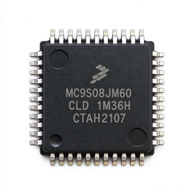
MC9S08JM8CLD - 8-Bit 48MHz USB MCU | NXP Semiconductors
MC9S08JM8CLD

MC9S08JM8CLD - 8-Bit 48MHz USB MCU | NXP Semiconductors

The NXP Semiconductors MC9S08JM8CLD is an 8-bit S08 microcontroller with a 48 MHz processor, 8 KB of flash memory, 1024 bytes of RAM, and on-chip USB 2.0 full-speed device connectivity in a 44-LQFP 10 x 10 mm package. It is designed for compact embedded systems that require USB communication without the complexity of a higher-performance 32-bit architecture. A microcontroller is a programmable semiconductor that combines a processor core, memory, and peripherals in one integrated circuit. The MC9S08JM8CLD belongs to the S08 family of 8-bit microcontrollers and is positioned as an economical USB-capable controller for industrial, consumer, and portable-device designs. Its integrated USB interface simplifies USB-to-serial data exchange while conserving board space and reducing the number of external interface components. The principal features include an S08 8-bit core operating at 48 MHz, 8 KB of flash program memory, 1024 bytes of RAM, and USB 2.0 full-speed device support. The 44-LQFP package provides 44 external leads and is suitable for automated board assembly. The device supports 3.3 V and 5 V operating environments, allowing its use in both legacy 5 V USB designs and modern 3.3 V systems. Exact peripheral inventories, electrical limits, and timing parameters should be confirmed in the manufacturer datasheet before final design release. The S08 architecture uses an 8-bit processing model suited to control tasks, USB data handling, status reporting, and communication management rather than graphics, high-bandwidth storage, or intensive signal processing. Its integrated USB controller makes it useful as the principal application processor in compact USB peripherals, where a higher-performance MCU would add cost or design complexity without providing a corresponding system benefit. Typical uses include USB-connected data acquisition devices, portable instrumentation, configuration tools, simple human-interface peripherals, and industrial service interfaces. Designers can place the device between a USB connector and the controlled subsystem, then use its on-chip USB peripheral to exchange serial data while timers, communications peripherals, and general-purpose I/O handle local control functions. When laying out the board, route USB D+ and D- as a controlled impedance differential pair and minimize the distance between the controller, connector, and protection components. Confirm the pin-multiplexing and alternate-function requirements in the manufacturer pin-description table, and account for every supply and ground connection before routing. Because the device is listed as end of life, new production designs should include a formal lifecycle and sourcing review. This page combines the manufacturer's lifecycle information, distributor specifications, technical search results, and application-oriented engineering guidance to clarify where the MC9S08JM8CLD fits. It also distinguishes verified drop-in options from merely similar devices, helping engineers avoid assuming that equal flash capacity and package size guarantee peripheral, pinout, timing, or software compatibility.

Angebot Kontakt
MC9S08JR12FAE - 8-Bit S08 MCU, 12KB Flash, 48-LQFP | NXP
MC9S08JR12FAE

MC9S08JR12FAE - 8-Bit S08 MCU, 12KB Flash, 48-LQFP | NXP

The NXP MC9S08JR12FAE is an 8-bit S08-family microcontroller with 12KB of Flash program memory, offered in a 48-pin LQFP (7x7 mm) package. Designed for cost-sensitive embedded applications, it integrates a 27 MHz S08 CPU core, on-chip peripherals, and low-power operating modes aimed at industrial control, metering, and human-machine interface (HMI) designs. The part targets small-form-factor board designs where BOM size and power budget matter as much as raw performance. A microcontroller (MCU) is a single-chip computer that integrates a CPU core, non-volatile program memory (Flash), volatile working memory (RAM), and a mix of analog and digital peripherals such as timers, ADC, communication ports (UART, SPI, I2C), and GPIO. The S08 family from NXP (originally Freescale) occupies the low-power 8-bit segment of the broader MCU hierarchy (8-bit -> microcontroller -> embedded processor -> semiconductor), competing against AVR and PIC families in cost-optimized designs. Key features include 12KB on-chip Flash (organized as 12K x 8), 1KB of SRAM, multiple low-power STOP and WAIT modes, an internal clock source, a multi-channel 10/12-bit ADC, timers, and standard serial peripherals. The 48-LQFP package exposes generous I/O count for keypad scan, LCD drive, or sensor interface tasks typical in white goods and metering end products. Architecturally, the S08 core uses a von Neumann-style memory map with a unified Flash/EEPROM-style block and BGSC (background debug controller) for in-circuit programming and debug via a single-wire BDM interface. The internal clock, watchdog, and reset circuitry reduce external component count, supporting compact two-layer PCB layouts. Typical applications include industrial control panels, IoT edge sensor nodes, low-end motor control, electronic metering, smart appliances, and battery-powered HMI boards. The combination of small Flash, low STOP-mode current, and 48-LQFP footprint makes it a go-to part for replacement of older HC08 designs. When designing with this part, ensure the VD supply is decoupled with a 100 nF plus 4.7 uF bulk cap near the pins. Leave the RESET pin pulled up externally if the internal pull-on-device is not enabled in software, and respect the 2.7 V minimum supply for Flash programming operations. This page synthesizes NXP official specifications, current distributor pricing, drop-in compatible alternatives, and engineering design notes not found in the standalone datasheet document.

Angebot Kontakt
MC9S08JS16CWJ - 8-bit S08 USB MCU, 16KB Flash, 48MHz | NXP
MC9S08JS16CWJ

MC9S08JS16CWJ - 8-bit S08 USB MCU, 16KB Flash, 48MHz | NXP

The NXP MC9S08JS16CWJ is an 8-bit HCS08 (S08) family microcontroller featuring an integrated USB 2.0 full-speed device controller with on-chip USB transceiver, 16KB of flash program memory, and a 48 MHz CPU core delivering a 24 MHz internal bus. It is housed in a 20-pin SOIC (SOIC W) wide-body package suitable for industrial temperature ranges of -40C to +85C, with single-supply operation from 2.7 V to 5.5 V. What is an S08 8-bit microcontroller? The S08 is NXP's (formerly Freescale) 8-bit CISC microcontroller family built around the HCS08 CPU core, which succeeds the legacy HC08 family with an enhanced instruction set, hardware multiply/divide in the accumulator, and a richer peripheral integration strategy. An 8-bit MCU like the MC9S08JS16CWJ is typically chosen when the application requires simple deterministic firmware, USB connectivity, low cost, and easy development with CodeWarrior or the newer Eclipse-based S08 toolchains, rather than the raw processing throughput of a 32-bit Cortex-M device. Key features that differentiate this part include the integrated USB 2.0 full-speed (12 Mbps) device controller with an on-chip transceiver that eliminates external USB PHY components, 16 KB of flash with 512 bytes of RAM, multiple serial interfaces (SCI, SPI), and a hardware LIN bus capability for automotive sub-bus applications. The part operates from a single 3.0 V or 5.0 V supply rail and supports background debugging via the standard BDM interface. The on-chip regulator and low-power run/wait/stop modes suit battery-powered USB peripherals such as HID input devices and low-data-rate industrial sensors. The MC9S08JS16CWJ combines a 48 MHz CPU, 24 MHz bus, hardware multiply, and integrated USB into a compact 20-pin SOIC footprint, simplifying BOM and PCB area versus an external MCU + ULPI/UTMI PHY architecture. The on-chip pull-up on the D+ line and integrated 3.3 V USB regulator are particularly valuable for cost-sensitive USB peripheral designs. Typical applications include USB HID input devices (keyboards, mice, custom HID peripherals), USB-to-UART bridge dongles, low-cost industrial sensor interfaces that expose a USB CDC or vendor-class endpoint, and LIN-to-USB or RS-232-to-USB protocol-converter dongles. The wide operating voltage and integrated transceiver make it a strong fit for any USB peripheral that must interface with a PC host. When designing with this part, ensure that the USB D+ pull-up (1.5 kohm to 3.3 V) is enabled in firmware after bus attach is desired, and add ESD protection (such as a USBLC6-2SC6 array) on D+/D- lines for production robustness. Decouple VDD and the USB voltage-domain pins with 100 nF and 4.7 uF ceramic capacitors placed within a few millimetres of the IC pins, and follow standard USB 2.0 differential-pair impedance (90 ohm differential) for the D+/D- traces. This page synthesizes distributor pricing, drop-in alternatives from the JS8/JS16 family and cross-brand pin-compatible USB MCUs, and practical design notes not found in the manufacturer datasheet. Pricing is referenced as of 2026-10-10 from DigiKey and Mouser.

Angebot Kontakt
MC9S08JS16LCFK - 8-bit USB MCU 16KB Flash 48MHz | NXP
MC9S08JS16LCFK

MC9S08JS16LCFK - 8-bit USB MCU 16KB Flash 48MHz | NXP

The NXP MC9S08JS16LCFK is an 8-bit S08-core microcontroller with 16KB (16K x 8) Flash memory, 512 bytes of RAM, a 48MHz CPU (24MHz internal bus clock), and a full-speed USB 2.0 device controller with integrated transceiver, housed in a 24-pin VQFN (5x5 mm) exposed-pad package with 14 GPIO. An 8-bit microcontroller is a self-contained computing IC that integrates a processor core, program memory, data memory, and peripherals on a single chip. The S08 (HCS08) family sits within NXP's broader Freescale MCU hierarchy: HCS08 -> 8-bit microcontroller -> embedded processor -> semiconductor. 8-bit MCUs dominate cost-sensitive embedded control tasks such as USB peripherals, appliance control, and simple human-interface devices. The defining feature of the JS16 family is its full-speed USB 2.0 device controller with an on-chip USB transceiver, eliminating external transceiver components and reducing bill-of-materials cost. Supporting peripherals include LVD (low-voltage detect), POR (power-on reset), and PWM modules, with connectivity via LINbus, SCI, and SPI in addition to USB. An internal oscillator option removes the need for an external crystal in many designs. The HCS08 CPU executes at up to 48MHz with a 24MHz internal bus, delivering efficient interrupt-driven operation for USB endpoint servicing. The 16KB Flash accommodates USB stack firmware alongside application code, while 512 bytes of RAM handle endpoint buffers and application variables. The 24-VQFN exposed-pad package provides compact 5x5 mm footprint suitable for space-limited PC peripheral boards. Typical applications include affordable PC peripherals such as HID devices, USB dongles, sensor bridges, and game controllers - applications the NXP product page explicitly targets. The integrated USB transceiver makes it a strong fit for compact, low-cost USB-to-UART or USB-to-SPI bridges. Designers should budget RAM carefully: with only 512 bytes, USB endpoint buffering and application data must be allocated conservatively. Enabling the internal oscillator saves a crystal but verify USB timing tolerance in your design. This page synthesizes distributor pricing, verified specifications from the NXP MC9S08JS16 datasheet, drop-in family alternatives, and practical design notes not found in the manufacturer datasheet alone.

Angebot Kontakt
MC9S08JS8CFK - 8-Bit 48MHz USB 2.0 MCU | NXP Semiconductors
MC9S08JS8CFK

MC9S08JS8CFK - 8-Bit 48MHz USB 2.0 MCU | NXP Semiconductors

The NXP Semiconductors MC9S08JS8CFK is an 8-bit HCS08 microcontroller with a 48 MHz CPU, 8 KB of Flash program memory and USB 2.0 full-speed device support in a 24-HVQFN package measuring 5 mm by 5 mm. It combines a 24 MHz internal bus with 512 bytes of RAM and an integrated USB transceiver for compact USB-connected control designs. An HCS08 microcontroller is an 8-bit embedded-control processor within the broader microcontroller and semiconductor hierarchy. The S08JS family is intended for applications that need moderate processing performance, fast flash execution and direct USB connectivity without requiring a separate transceiver. Its bus-oriented architecture supports peripheral integration, event-driven control and low-cost USB peripheral designs. Key device characteristics include an 8-bit CPU operating at up to 48 MHz, 8 KB of Flash organized as 8192 words, 512 bytes of RAM, a 24 MHz internal bus and a maximum supply voltage of 5.5 V. The listed operating temperature range is -40 °C to +85 °C, making the device suitable for industrial-temperature control equipment. The JS family also provides a full-speed USB 2.0 device controller with an on-chip transceiver. The 48 MHz CPU provides useful headroom for protocol handling, state-machine control and peripheral servicing compared with slower 8-bit MCUs. Flash-resident firmware supports fast start-up, while the integrated USB transceiver reduces board area by removing the need for a discrete USB PHY. The small 5 mm by 5 mm package supports compact consumer, industrial and communications-oriented boards. Typical uses include USB-connected data acquisition, HID peripherals, configuration tools, industrial control panels and compact consumer accessories. A system requiring direct USB enumeration can connect the MCU to a USB Type-A or Type-C interface through the appropriate protection, routing and connector implementation. Designers should confirm the exact 24-pin signal map, supply operating range and peripheral assignments in the manufacturer datasheet before layout. Decoupling, USB impedance routing and firmware timing remain critical. When upgrading, verify USB enumeration behavior, interrupt priorities and any peripheral differences rather than treating a shared package as automatic software compatibility.

Angebot Kontakt
MC9S08JS8CWJ - 8-Bit 48MHz MCU, 8KB Flash | NXP
MC9S08JS8CWJ

MC9S08JS8CWJ - 8-Bit 48MHz MCU, 8KB Flash | NXP

The NXP Semiconductors MC9S08JS8CWJ is an 8-bit HCS08 microcontroller with a 48 MHz CPU, 8 KB of Flash program memory, and a 20-pin SOIC package. It operates from a 3.3 V or 5 V supply and is identified in the verified sources as an S08JS-series MCU with USB 2.0 device connectivity, serial interfaces, and 14 I/O pins. An HCS08 microcontroller is an embedded-control semiconductor that combines a CPU, program memory, data memory, peripherals, and I/O in one integrated device. The S08 family uses an 8-bit architecture intended for cost-sensitive embedded systems, where deterministic control, low component count, and simple firmware execution are more important than workstation-class processing performance. Key verified features include an 8-bit HCS08 central processing unit, operation up to 48 MHz, an internal bus listed at 24 MHz, 8 KB Flash organized as 8K x 8, and 512 x 8 bits of RAM. The source data also identifies USB 2.0, LINbus, SCI, SPI, PWM, low-voltage detection, power-on reset, and 14 I/O capabilities, making the device suitable for connected peripheral control. The MC9S08JS8CWJ is supplied in a 20-SOIC package. The verified datasheet listing describes the device as an 8-bit MCU with 8 KB Flash and USB 2.0, while distributor data identifies the same 20-SOIC package and 48 MHz speed. Because the supplied evidence does not provide a complete manufacturer pin table, individual pin names are not asserted here. Typical uses include USB-connected control nodes, industrial interface modules, serial bridges, instrumentation peripherals, and compact consumer or embedded-control products. The 3.3 V and 5 V supply descriptions support both legacy 5 V and lower-voltage system designs, subject to the complete manufacturer electrical limits. The principal design consideration is not to infer USB, timing, or peripheral compatibility from a similar S08JS part. Firmware, pin multiplexing, clock configuration, USB behavior, and reset requirements must be verified against the exact manufacturer documentation. This page combines verified source specifications, sourcing information, lifecycle context, and engineering-oriented selection guidance.

Angebot Kontakt
MC9S08JS8LCFK - 8KB Flash USB MCU 48MHz | NXP S08JS
MC9S08JS8LCFK

MC9S08JS8LCFK - 8KB Flash USB MCU 48MHz | NXP S08JS

The NXP MC9S08JS8LCFK is an 8-bit S08JS microcontroller with an integrated USB 2.0 full-speed device controller, 8KB of Flash program memory, and an on-chip USB transceiver, housed in a 24-pin HVQFN (5x5 mm) package with an exposed thermal pad. It operates at up to 48 MHz internal bus frequency and supports both 3.3V and 5V supply rails, making it a one-chip solution for USB peripherals that previously required an external USB transceiver and a separate MCU. An 8-bit microcontroller (MCU) is a small computing system-on-chip that integrates a CPU, memory (Flash/RAM), and configurable peripherals onto a single silicon die. The HCS08 CISC architecture used in the S08 core family is a low-power, deterministic instruction set that simplifies firmware development for cost-sensitive embedded products. Within the broader taxonomy, the MC9S08JS8LCFK sits as: 8-bit MCU -> microcontroller -> integrated circuit -> semiconductor. By integrating a USB 2.0 transceiver and PHY directly on die, NXP helps engineers reduce BOM cost and PCB area versus two-chip USB designs. Key features of the MC9S08JS8LCFK include: 8 KB Flash program memory for USB class firmware, integrated USB 2.0 full-speed (12 Mbps) device controller with on-chip transceiver, 24-pin HVQFN 5x5 mm package with thermal pad, industrial temperature grade support, and on-chip debug (BKGD) plus enhanced clock generation. The integrated USB PHY eliminates external pull-up resistors and the off-chip transceiver IC typically required by legacy USB designs. The HCS08 core executes most instructions in 1-2 bus cycles, and an internal 48 MHz clock drives the USB module to maintain precise 12 Mbps full-speed signaling. The 8KB Flash is in-system programmable via the background debug mode (BDM), supporting field updates. Multiple low-power modes (Stop, Wait, Run) plus an internal low-power oscillator optimize battery-powered USB peripherals. Typical applications include USB Human Interface Devices (HID) such as keyboards, mice, and game controllers, USB-to-UART bridge dongles, USB class-compliant barcode scanners, industrial USB sensors, low-cost USB peripherals and consumer accessories where a 48 MHz 8-bit core is sufficient and BOM cost dominates. When designing with this part, ensure the D+ pull-up resistor (1.5 kohm to 3.3V) is correctly placed, the VBUS pin is properly decoupled, and the exposed thermal pad is soldered to the ground plane for thermal and electrical performance. The 24-pin HVQFN requires careful PCB layout - the e-pad must have multiple thermal vias to dissipate heat. This page synthesizes drop-in alternatives, comparison tables, design notes, and pricing not aggregated elsewhere; engineers can quickly determine whether the MC9S08JS8LCFK fits their USB peripheral design versus the larger JS16, SH8, or QG8 family siblings.

Angebot Kontakt
MC9S08LC36LH - 8-bit S08LC MCU, 36KB Flash, 40MHz, LCD | NXP
MC9S08LC36LH

MC9S08LC36LH - 8-bit S08LC MCU, 36KB Flash, 40MHz, LCD | NXP

The NXP MC9S08LC36LH is an 8-bit HCS08-family microcontroller (S08LC sub-family) with 36KB on-chip Flash, an integrated LCD controller, and a 40-MHz CPU core, packaged in a 64-pin LQFP (10x10 mm). It targets battery-powered and handheld applications requiring an integrated segment-LCD driver combined with the low-power capabilities of the S08 platform. An HCS08 microcontroller is a member of the 8-bit MCU category that uses the HC08 instruction set with extensions for low-power operation and on-chip peripherals; within the power management taxonomy, an 8-bit MCU belongs to the broader microcontroller > embedded controller > semiconductor device hierarchy. The MC9S08LC36LH combines CPU, memory (Flash + RAM), analog (ADC), communications (SCI/SPI/I2C), and LCD driving in a single chip, reducing external component count for cost-sensitive LCD human-machine-interface designs. Key features confirmed from the verified datasheet extract include 40 MHz maximum CPU clock, 36 KB program Flash, an integrated LCD controller (the defining differentiator of the S08LC sub-family), 18 general-purpose I/O ports, and a 1.8V to 3.6V supply-voltage operating range. The device is specified for the LFQP / LQFP-64 (10 mm x 10 mm, 0.5 mm pitch, 1.40 mm height) package and is described as the first LCD S08 8-bit MCU in NXP's (formerly Freescale) portfolio aimed at battery-powered and handheld segments. Architecturally, the S08LC integrates an HC08-compatible core augmented with a Background Debug mode (BGND) instruction, a Background Debug System (BDS) for in-circuit debugging, and breakpoint capability to allow single breakpoint setting during in-circuit debugging. On-chip peripherals typically found in the family include timers (TPM), real-time interrupt, ADC, and multi-master I2C plus SPI and SCI for asynchronous/synchronous serial. Typical applications include battery-powered handheld instruments (medical meters, remote controls, utility readers), segment-LCD display modules (appliance controls, thermostats, point-of-sale terminals), and consumer / industrial HMI where a single-chip LCD + MCU solution reduces BOM. Its 1.8V minimum supply supports single-cell Li-primary or 2x AA Alkaline chemistries. When designing with this MCU, careful decoupling (100 nF + bulk) is required near each VDD/VSS pair, and the LCD segment/Common pins require proper bias-resistor networks (typically a resistor ladder or charge-pump-based bias generation) to achieve specified contrast and low-quiescent LCD waveforms. This page synthesizes the official Freescale/NXP datasheet specifications, distributor pricing as of 2026-10-18, and drop-in alternative guidance not always found on the manufacturer product page.

Angebot Kontakt
MC9S08LC36LK - 8-bit S08 MCU, 36KB Flash, LCD Driver | NXP
MC9S08LC36LK

MC9S08LC36LK - 8-bit S08 MCU, 36KB Flash, LCD Driver | NXP

The NXP (Freescale) MC9S08LC36LK is an 8-bit HCS08 microcontroller with an integrated LCD controller, 36KB of Flash memory, a 40 MHz internal bus clock capability, and an 80-pin LQFP (12x12 mm) package operating from a 1.8V to 3.6V supply. An 8-bit microcontroller is a single-chip computing device whose CPU processes 8-bit data words. The MC9S08LC36 belongs to the broader HCS08 family, which sits within NXP's 8-bit MCU portfolio under the microcontrollers and embedded processors hierarchy. The S08LC family is notable as the first S08-based 8-bit MCU family integrating an on-chip LCD driver, targeting battery-powered and handheld products where segment or small-matrix glass displays are required. Key features include 36KB (36K x 8) of in-circuit reprogrammable Flash, a 40 MHz HCS08 CISC core executing the HC08 instruction set with an added BGND instruction, an integrated LCD controller, a 10-bit ADC, and serial peripherals including I2C, SPI, and PWM timers. The wide 1.8V to 3.6V operating range supports both 2.5V and 3.3V system rails, making the part suitable for direct battery operation. Architecturally, the HCS08 core provides background debugging (single-wire BGND-based debug), breakpoint capability for in-circuit development, and low-power wait and stop modes that pair well with the LCD controller for battery-operated metering and handheld display products. The 80-pin LQFP measures 10 x 10 mm body (12 x 12 mm footprint, 1.40 mm height, 0.50 mm pitch) and provides 18 I/O ports plus dedicated LCD segment lines. Typical applications include battery-powered handheld instruments, utility metering displays, small appliances with segment LCDs, and low-power consumer devices where an LCD driver, ADC, and serial interfaces must coexist in a single low-cost chip. Design consideration: because this device is End of Life per the NXP product page, new designs should verify remaining distributor stock and plan a drop-in family alternative such as the MC9S08LC60LK, which shares the same 80-pin LQFP footprint with 60KB Flash. This page synthesizes distributor pricing, drop-in same-family alternatives, and practical design guidance not found in a single manufacturer datasheet, with all specifications cross-checked against NXP and distributor listings as of 2026-10-18.

Angebot Kontakt
MC9S08LC60LH - 8-bit S08 MCU, 60KB Flash, LCD, USB, CAN | NXP
MC9S08LC60LH

MC9S08LC60LH - 8-bit S08 MCU, 60KB Flash, LCD, USB, CAN | NXP

The NXP MC9S08LC60LH is a 40-MHz 8-bit HCS08 microcontroller with 60 KB Flash, an integrated LCD controller, USB and CAN connectivity, housed in a 64-pin LQFP (10x10 mm) package. It is part of the Freescale/NXP S08LC family targeting low-power segment-LCD and human-machine interface applications. An 8-bit MCU (microcontroller unit) is a single-chip computer that integrates a CPU, memory, and peripherals on one die. The HCS08 core is a von-Neumann 8-bit CPU executed from a common Flash/ROM address space, designed for predictable interrupt latency and ultra-low standby power. Microcontrollers sit at the foundation of every embedded system; 8-bit variants are favored when cost, deterministic behavior, and peripheral integration (LCD, USB, CAN) outweigh raw compute throughput. Key features of the MC9S08LC60LH include 60 KB on-chip Flash, 4 KB RAM, an internal LCD driver with up to 8 backplanes and configurable segment count, a USB 2.0 full-speed device controller, a CAN 2.0 A/B module, two SCI, one SPI, and up to 18 GPIO pins. The CPU runs up to 40 MHz (20 MHz bus) from a 1.8 V to 3.6 V supply, supporting both lithium-cell and 3.3 V regulated rails. Architecturally, the S08LC uses the HCS08 instruction set (object-code compatible with HC08 plus BGND for debugging), a 3-stage pipeline, and a multi-tier clock gating scheme that allows peripherals to be gated individually during STOP modes. The integrated LCD charge pump supports both glass types and contrast over temperature. Typical applications include metering and instrumentation, medical devices, white-goods HMIs, industrial control panels, and consumer products requiring segment-LCD displays with USB connectivity. The CAN interface makes it attractive in automotive body and appliance networks. When designing with this part, allocate PCB area for the LCD segment pins (which form a large portion of the LQFP-64 ballout) and place the external 32.768 kHz crystal close to the XTAL pins to minimize stray capacitance. This page synthesizes distributor pricing, drop-in alternatives, and practical design notes not found in the manufacturer datasheet.

Angebot Kontakt
MC9S08LC60LK - 8-bit S08 MCU 60KB Flash LCD | NXP
MC9S08LC60LK

MC9S08LC60LK - 8-bit S08 MCU 60KB Flash LCD | NXP

The NXP Semiconductors MC9S08LC60LK is an 8-bit microcontroller (MCU) based on the HCS08 (S08) core, running at up to 40 MHz, with 60 KB of Flash memory and an integrated LCD controller, housed in an 80-pin LQFP (LFQP, 12x12 mm, 0.5 mm pitch) package. An 8-bit microcontroller is an integrated circuit that combines a processor core, memory (Flash, RAM), and peripherals such as timers, serial interfaces, and analog comparators on a single chip. Within the system hierarchy, an MCU sits at the embedded control level: semiconductor -> microcontroller (MCU) -> 8-bit MCU family -> NXP S08 family -> S08LC LCD series. The S08LC series is notable as NXP's first LCD-capable S08 8-bit MCU, targeted at battery-powered and handheld applications. Key features include the 40 MHz HCS08 CPU with HC08 instruction set compatibility plus an added BGND instruction, 60 KB (60K x 8) of Flash program memory, an integrated LCD driver that offloads segment driving from software, and a wide supply voltage range of 1.8 V to 3.6 V suitable for battery operation. A background debugging system with single-breakpoint capability supports in-circuit development without consuming chip resources. Technically, the device uses the enhanced HCS08 architecture with reduced instruction overhead, internal oscillator options, and low-power modes designed for handheld instruments where display content and battery life dominate the design. The on-chip analog comparator (ACMP) supports simple voltage monitoring and threshold detection without an external comparator IC. Typical applications include handheld meters and instruments with LCD displays, battery-powered consumer devices, and low-cost industrial panels where an integrated LCD driver replaces a separate segment-driver IC. A key design consideration: NXP lists this product as End of Life (EOL), so new designs should plan for last-time-buy quantities or migration within the S08 family. Verify remaining stock and the official PCN before committing the footprint to new layouts. This page synthesizes distributor pricing, lifecycle status, and drop-in alternative analysis not found in the manufacturer datasheet alone, with all data verified against NXP and distributor listings as of 2026-10-18.

Angebot Kontakt
MC9S08LG16CLH - 8-bit LCD MCU, 18KB Flash, 40MHz | NXP
MC9S08LG16CLH

MC9S08LG16CLH - 8-bit LCD MCU, 18KB Flash, 40MHz | NXP

The NXP MC9S08LG16CLH is an 8-bit HCS08 segment-LCD microcontroller delivering 40 MHz CPU performance with 18 KB of on-chip Flash and a 64-pin LQFP (10x10 mm) package. It belongs to the cost-effective S08LG family, designed to drive liquid crystal displays with up to 296 segments while operating from a wide 2.7 V to 5.5 V supply. A segment-LCD MCU is a specialized 8-bit microcontroller that integrates a dedicated LCD driver, charge pump, and bias-generation circuitry alongside a general-purpose CPU. The device hierarchy is: 8-bit MCU -> segment LCD MCU -> HCS08 family -> S08LG sub-family -> embedded control IC. Compared with discrete MCU-plus-LCD-driver designs, the MC9S08LG16CLH reduces PCB area, BOM count, and BOM cost for applications that only need character or segment displays rather than graphical TFT panels. Key features include the HCS08 CPU core at 40 MHz bus speed, 18 KB Flash, 2 KB RAM, an internal oscillator, an integrated LCD driver supporting up to 296 segments across 8 backplanes, multiple timers (MTIM and TPM), an analog-to-digital converter, and an on-chip in-circuit emulator (ICE) for real-time debug. The wide 2.7 V to 5.5 V operating range and industrial temperature grade (-40 C to +85 C) make the part suited to factory-floor and appliance environments. Architecturally, the S08LG family uses a von-Neumann bus with Flash-resident vector table, low-power wait and stop modes, and a switchable internal 32 kHz / 1 MHz / bus-frequency clock. The integrated LCD controller supports static, 2x, 3x, 4x, 6x, and 8x multiplexed modes with selectable bias and contrast, eliminating the need for an external LCD bias-voltage network. Typical applications include electric meters, home appliances, HVAC user interfaces, white-goods control panels, entry-level instrument clusters, and any cost-sensitive human-machine interface (HMI) that uses a segment LCD. When designing with this part, choose the LQFP-64 footprint early so PCB escape routing for the 30+ segment pins does not force a re-spin. This page synthesizes NXP datasheet values, current distributor pricing, drop-in alternatives, and practical design notes that go beyond the manufacturer datasheet, helping engineers evaluate the MC9S08LG16CLH for new designs and migration paths from its S08LG family siblings.

Angebot Kontakt
MC9S08LG32CLF - 40MHz 8-Bit 32KB Flash LCD MCU | NXP
MC9S08LG32CLF

MC9S08LG32CLF - 40MHz 8-Bit 32KB Flash LCD MCU | NXP

The NXP Semiconductors MC9S08LG32CLF is an 8-bit HCS08 microcontroller with a 40 MHz CPU, 32 KB of flash memory, and 48-LQFP (7x7 mm) packaging optimized for segment-LCD applications. It operates in the 3.3 V and 5 V supply range identified in the distributor data and can drive segment-LCD displays for industrial and automotive products. The device is marked NRND on NXP's product page. A segment-LCD microcontroller is a specialized embedded-control device that combines a general-purpose CPU with display-segment drivers. It reduces the component count in meters, appliances, HVAC controls, and instrument clusters because many display outputs are generated internally rather than through separate external driver ICs. The MC9S08LG family is positioned within the hierarchy of MCU, embedded microcontroller, semiconductor, and general-purpose control IC. Key verified features include an 8-bit HCS08 central processing unit, operation up to 40 MHz, 32 KB of flash, and support for LCDs with up to 296 segments. The 48-LQFP package provides 48 external terminals and suits cost-sensitive designs that need a conventional surface-mount footprint. An on-chip in-circuit emulator is also identified in the retrieved technical material, supporting development and debugging workflows. The MC9S08LG32CLF belongs to the MC9S08LG32/LG16 series and is supplied in the LF, 48-LQFP configuration described by the distributor records. Its 5 V segment-LCD positioning makes it relevant to direct-drive display products, especially electric metering, home appliances, HVAC systems, and entry-level instrument clusters. Availability and lifecycle planning should account for the NRND designation. A typical design connects the MCU to a segment-LCD glass, external sensing inputs, application controls, and programming or debug circuitry. The exact pin assignments, LCD mapping, memory organization, electrical limits, and programming details must be confirmed against the NXP MC9S08LG32 Series data sheet before schematic capture or PCB release. Because the verified data does not establish a complete set of pin-level electrical limits or application-specific timing margins, designers should not infer missing values. Validate the selected package, display configuration, clock setup, and all peripheral assignments against the manufacturer documentation. This page consolidates verified manufacturer and distributor information, pricing context, application guidance, and strict same-package replacement analysis for engineers evaluating the MC9S08LG32CLF.

Angebot Kontakt
MC9S08LG32CLK - 8-Bit 40MHz 32KB Flash LCD MCU | NXP
MC9S08LG32CLK

MC9S08LG32CLK - 8-Bit 40MHz 32KB Flash LCD MCU | NXP

The NXP Semiconductors MC9S08LG32CLK is an 8-bit HCS08 segment-LCD microcontroller with 32KB of flash memory, operation up to 40MHz, and an 80-pin LQFP package. It supports 3.3V and 5V operation, integrated analog features, and LCD segment drive suitable for industrial and automotive control systems. The MC9S08LG32CLK belongs to the NXP MC9S08LG family of 8-bit microcontrollers with integrated liquid-crystal display drive. An HCS08 MCU combines a CPU, embedded flash, RAM, timers, serial interfaces, analog peripherals, and LCD-drive resources in one device. This family targets applications such as electric meters, home appliances, HVAC systems, and entry-level instrument clusters. Key features include an 8-bit HCS08 central processing unit, clock operation to 40MHz, 32KB of flash memory, 3.3V/5V operation, flexible pin functionality, and support for segment LCDs with up to 296 segments. The 80-LQFP package provides the pin count needed for display and control connectivity in compact embedded systems. The device is designed for low-cost, display-oriented embedded control. Its 5V segment-LCD capability and integrated analog functions allow designers to build meters, appliance controls, and HVAC interfaces without adding a separate display driver. The HCS08 architecture supports deterministic control while keeping firmware and hardware integration compact. Typical applications include electric meters, household appliances, HVAC controllers, industrial instrumentation, automotive control panels, and entry-level instrument clusters. The LCD-driver resources are particularly useful when a large number of segments must be scanned directly. When designing a circuit, confirm the exact LCD segment and pin assignment, operating voltage, clock configuration, and external component requirements in the MC9S08LG32 datasheet. Use the specified decoupling and programming/debug interfaces rather than assuming compatibility with a different MCU pinout.

Angebot Kontakt
MC9S08LH36CLK - 8-bit S08 MCU 40MHz 36KB Flash | NXP
MC9S08LH36CLK

MC9S08LH36CLK - 8-bit S08 MCU 40MHz 36KB Flash | NXP

The NXP (Freescale Semiconductor) MC9S08LH36CLK is an 8-bit HCS08 microcontroller IC delivering up to 40 MHz CPU frequency, 36 KB (36K x 8) FLASH program memory, and 37 general-purpose I/O lines, housed in an 80-pin LQFP (14 x 14 mm) surface-mount package. An 8-bit microcontroller is an integrated circuit that combines a processor core, memory, and peripherals on a single chip, forming the lowest tier of the embedded-processor hierarchy (MCU -> embedded processor -> semiconductor). The S08 (HCS08) family from Freescale/NXP is a widely deployed 8-bit architecture used in cost-sensitive control tasks, sitting alongside families such as the HC08 legacy line and competing 8051 and PIC8 architectures. Key features of the MC9S08LH36CLK include a 2.1 V to 3.6 V single-supply operating range, 36 KB of in-system-programmable FLASH with sector erase, and operation up to 40 MHz CPU clock (16 MHz bus operation is cited in some distributor parametric listings). The large 37-I/O count and 80-pin LQFP footprint make it suitable for designs needing many parallel control lines without port expanders. Technically, the device is built around the HCS08 central processor unit with background debug mode (BDM) for non-intrusive in-circuit flashing and debugging. Distributor data describes lifecycle stage as ACTIVE, and the part is RoHS compliant per parametric listings. The LQFP-80 (14 x 14 mm) body provides 0.5 mm lead pitch for dense two-layer and four-layer PCB designs. Typical applications include industrial control panels, consumer appliance control, LCD-segment-driven human-machine interfaces, and battery-powered instrumentation where 3V logic and low-cost 8-bit processing are sufficient. Design consideration: verify whether your design requires the 40 MHz CPU-rated grade or only 20 MHz operation at 2.1 V, since available bus frequency scales with supply voltage per the S08 family datasheet. This page adds value beyond the manufacturer datasheet by consolidating distributor stock locations, a drop-in same-family alternative comparison, and practical sourcing notes for this Rochester Electronics-supported NXP part.

Angebot Kontakt
MC9S08LH64CLH - 40MHz 64KB Flash 8-Bit MCU | NXP
MC9S08LH64CLH

MC9S08LH64CLH - 40MHz 64KB Flash 8-Bit MCU | NXP

NXP Semiconductors MC9S08LH64CLH is an 8-bit S08LH-series microcontroller operating at up to 40 MHz, with 64 KB of Flash memory and a 64-pin LQFP package measuring 10 mm by 10 mm. The device is positioned for low-power embedded systems that need extended flash capacity, an LCD driver, and improved analog-to-digital converter accuracy. A microcontroller is a programmable integrated circuit that combines a CPU core, memory, input/output ports, timers, communication interfaces, and analog peripherals on one device. The S08LH family belongs to the 8-bit MCU hierarchy and is intended to provide economical control for metering, medical instrumentation, industrial equipment, and battery-powered products. Rather than relying on multiple discrete components, an MCU centralizes computation, sensing, display control, and system communication. The verified product information identifies a 40 MHz maximum clock, 64 KB Flash, the S08 CPU core, and a 64-LQFP package. The family also features an LCD driver and increased ADC accuracy for medical and metering applications. Its ultra-low-power design targets energy-efficient operation, while the larger flash capacity provides more room for firmware than smaller members of the S08 family. The MC9S08LH64CLH is listed as NRND by NXP, meaning it is not recommended for new designs. Existing products may continue to use the device, but engineers should confirm lifecycle status, availability, and long-term sourcing before starting a new production program. The CLH orderable designation identifies a specific package and temperature-grade configuration, so replacement parts should be checked against the complete part-number decoding. Typical uses include utility meters, medical monitoring equipment, industrial controllers, sensor interfaces, and compact battery-powered instruments. The LCD driver is particularly useful for local alphanumeric or segmented displays, while the ADC supports analog measurement. Firmware should configure the required LCD segments, calibrate analog channels, and validate low-power behavior before deployment. Designers should follow the manufacturer datasheet for pin multiplexing, clock, decoupling, programming, and electrical limits. Because this is a 64-pin LQFP device, careful fan-out and routing are necessary to reduce assembly risk and preserve analog performance. This page consolidates verified lifecycle, package, memory, and application information while identifying where additional datasheet parameters are required.

Angebot Kontakt
MC9S08LH64CLK - 40MHz 64KB 8-Bit MCU | NXP
MC9S08LH64CLK

MC9S08LH64CLK - 40MHz 64KB 8-Bit MCU | NXP

The NXP Semiconductors MC9S08LH64CLK is a 40 MHz, 8-bit S08LK microcontroller with 64 KB of Flash memory, an LCD driver, and increased analog-to-digital converter accuracy for medical and metering applications. It is housed in an 80-LQFP package measuring 14 mm by 14 mm. The verified product information identifies an S08 core, 8-bit architecture, 64K x 8 Flash organization, and a 40 MHz maximum clock. A microcontroller is a programmable semiconductor that integrates a CPU, memory, peripherals, and input/output interfaces on one device. The S08 family belongs to the broader 8-bit embedded-controller hierarchy, where firmware is loaded into nonvolatile memory and the device controls sensors, displays, communication links, or actuators. The MC9S08LH64CLK therefore serves as the central controller in compact medical, metering, industrial, and human-interface systems rather than acting only as a general-purpose computing processor. Its headline features include a 40 MHz operating frequency, 64 KB Flash, an 80-LQFP package, an LCD driver, and enhanced ADC accuracy. The LCD-driver capability is useful for products that need a local segmented or matrix display without a separate display controller. The enhanced ADC accuracy makes the device relevant to measurement systems where signal-to-noise behavior and repeatability matter. The supplied data also identifies a 2.1 V to 3.6 V supply range and a 16 MHz clock-speed specification in one secondary listing, while the manufacturer and distributor results identify 40 MHz as the product headline frequency. The S08LK architecture is intended for embedded control rather than high-end application processing. Its 8-bit word size and on-chip peripherals make it suitable for control loops, user-interface handling, and low-to-medium-complexity sensing systems. Designers should verify the exact operating mode, clock configuration, ADC resolution, memory map, and peripheral availability against the manufacturer datasheet before final firmware and PCB release. Typical applications include medical instrumentation, metering equipment, programmable display controllers, industrial sensing terminals, and compact embedded control panels. In each case, the LCD driver can reduce external component count, while the ADC-related feature supports analog measurement. Firmware architecture, clocking, power budgeting, and display timing remain application-specific engineering decisions. The principal design consideration is to validate the complete operating envelope rather than relying only on the 40 MHz headline specification. Supply voltage, temperature grade, peripheral limits, pin multiplexing, LCD segment count, and analog accuracy determine whether the MC9S08LH64CLK fits a particular medical or metering design. A hardware drop-in alternative should not be assumed from package similarity alone. This page combines verified manufacturer and distributor information, practical application context, and explicit data-gap markers. It is designed to support component selection, sourcing, and engineering review without inventing specifications that were not present in the supplied evidence.

Angebot Kontakt
MC9S08LL16CGT - 8-Bit 20MHz 16KB MCU | NXP 48-QFN
MC9S08LL16CGT

MC9S08LL16CGT - 8-Bit 20MHz 16KB MCU | NXP 48-QFN

The NXP MC9S08LL16CGT is an 8-bit S08LL microcontroller operating up to 20 MHz, with 16 KB of Flash memory and 2 KB of RAM, in a 48-pin QFN exposed-pad package measuring 7 x 7 mm. It is designed for compact, low-cost embedded products requiring efficient control, low-power operation, and segment-LCD-oriented integration. A microcontroller is a programmable semiconductor that combines a CPU, memory, and peripherals on one integrated circuit. In the embedded-system hierarchy, the MC9S08LL16CGT belongs to the 8-bit microcontroller class and uses the HCS08 S08 core. Its combination of Flash program memory, RAM, communication peripherals, timing resources, and low-power features makes it suitable for applications where a higher-performance processor would add unnecessary cost or complexity. The verified product listing identifies the device as an 8-bit, 20 MHz MCU with 16 KB organized as 16K x 8 Flash and 2 KB RAM. The S08LL family is positioned for battery-powered equipment such as medical diagnostics and handheld appliances. Its 48-QFN exposed-pad package supports compact PCB placement while exposing a thermal and electrical connection area beneath the package; layout still requires exact compliance with the manufacturer land pattern and exposed-pad requirements. Typical designs use the MCU to supervise sensors, drive a segment LCD, scan input keys, manage a small motor or actuator, and communicate measurements through serial peripherals. The 20 MHz clock capability provides useful processing headroom for state-machine control and foreground routines. Firmware should nevertheless be organized to avoid unnecessary busy-waiting and should use the MCU's low-power modes when the product spends substantial time idle. Engineering attention belongs on decoupling, clock stability, exposed-pad layout, and firmware-compatible peripheral configuration. Place the required bypass capacitors close to the supply pins, follow the datasheet's recommended PCB stack-up and exposed-pad geometry, and verify programming and debug access before releasing a layout. Because the NXP product page identifies the device as End of Life, new production designs should also confirm availability and migration planning with the manufacturer. This page combines verified distributor specifications, manufacturer documentation, lifecycle information, and practical design guidance. It distinguishes verified facts from parameters that were not supplied, helping engineers assess fit without treating generic cross-reference results as guaranteed drop-in replacements.

Angebot Kontakt
MC9S08LL16CLF - 8-bit S08 MCU, 16KB Flash, 20MHz, 48-LQFP | NXP
MC9S08LL16CLF

MC9S08LL16CLF - 8-bit S08 MCU, 16KB Flash, 20MHz, 48-LQFP | NXP

The NXP MC9S08LL16CLF is a low-power 8-bit microcontroller from the S08LL family featuring an S08 CPU, 20MHz bus frequency, 16KB Flash program memory, an integrated segment LCD driver, and a high-precision real-time clock (RTC) in a 48-pin LQFP (7x7 mm) package. According to the manufacturer datasheet, the device operates from 2.1V to 3.6V and is engineered for ultra-low-power battery applications including portable medical diagnostics, handheld metering, and electronic shelf label displays. What is an 8-bit microcontroller? An 8-bit MCU is a single-chip computer with an 8-bit data path, integrating a CPU core, Flash program memory, RAM, peripherals, and interrupt logic on one die. The MC9S08LL16CLF belongs to the S08LL sub-family of NXP/Freescale HCS08 architectures, optimized for low-power segment-LCD-driven applications. In the broader taxonomy it sits within: microcontroller -> embedded processor -> semiconductor. Its integrated LCD driver and RTC eliminate the need for external display or clock ICs, reducing BOM cost and PCB area for portable battery-powered products. Key features include 16KB on-chip Flash, 2KB SRAM, an LCD driver supporting up to 8x28 or 4x32 segments, a real-time clock with calendar function, multiple low-power stop modes, and an internal oscillator that can reduce external component count. The 20MHz S08 CPU delivers approximately 2.7 MIPS/MHz throughput, adequate for low-speed control loops and human-interface tasks. Peripherals include multiple TPM timers, an ADC, I2C, SCI/UART, and SPI communication interfaces. The S08 core uses a von Neumann architecture with a CISC instruction set, simplifying software porting across the HCS08 family. The 48-LQFP package provides a standard 7x7 mm footprint with 0.5mm pitch for hand or reflow soldering, and the device supports industrial operating temperatures of -40C to +85C. Typical applications include medical glucose meters, blood-pressure monitors, portable gas/water/heat meters with LCD readout, thermostat controls, remote sensor displays, and battery-powered handheld appliances. The integrated LCD controller reduces system cost in any segment-display product, while the RTC enables timestamping of measurement events. When designing with the MC9S08LL16CLF, pay close attention to the LCD bias and charge-pump capacitor selection; the datasheet typical-application section shows specific cap values required for stable contrast under all operating temperatures. The RTC requires a 32.768 kHz crystal or external clock for timekeeping accuracy; software must initialize the LCD waveform and segment map registers before display activation. This page synthesizes distributor pricing, drop-in alternatives, and practical design notes not found in the manufacturer datasheet, giving engineers an actionable engineering reference for selecting, sourcing, and laying out the MC9S08LL16CLF.

Angebot Kontakt