Sensoren
Unterkategorien
Produkte (525)

IIS3DWBTR - Ultra-Wide Bandwidth 3-Axis Digital Vibration Sensor | STMicroelectronics
The STMicroelectronics IIS3DWBTR is an ultra-wide bandwidth, low-noise, 3-axis digital vibration sensor housed in a surface-mount LGA package with solder pads. It integrates a 3-Axis MEMS accelerometer with an on-chip digital interface supporting I2C and SPI, designed for high-fidelity vibration monitoring in industrial environments up to +105 C. According to the manufacturer datasheet, the device delivers a flat frequency response from DC to 6 kHz across all three axes (X, Y, Z), enabling accurate capture of mechanical vibrations in machinery and structural assets. Key specifications include selectable full-scale acceleration ranges of +/-2 g, +/-4 g, +/-8 g, and +/-16 g, along with ultra-low noise density of 75 ug/giB (in the high-performance mode). The on-chip ADC samples at up to 26.7 kHz with a 16-bit resolution, and the FIFO buffer holds up to 3 kB of programmable watermark data. The sensor operates from a 1.71 V to 3.6 V supply and includes a temperature sensor for thermal compensation. The IIS3DWBTR is a system-in-package (SiP) that combines the MEMS element and the ASIC in a single reflow-solderable land-grid-array module. The wide bandwidth, low noise, stable sensitivity, and the ability to operate over an extended temperature range make it particularly suitable for vibration monitoring of motors, pumps, fans, bearings, and structural components in Industry 4.0 deployments. Typical applications include condition monitoring and predictive maintenance in rotating machinery, vibration analysis in HVAC and building automation, motor control feedback loops, structural health monitoring of bridges and towers, and industrial IoT sensor nodes. The wide bandwidth also supports shock detection and seismic instrumentation. When designing with the IIS3DWBTR, place 100 nF decoupling capacitors as close as possible to the supply pins and follow the PCB layout guidelines in the manufacturer datasheet to minimize mechanical stress coupling and ensure accurate high-frequency vibration measurements. The 1.71 V minimum supply makes it directly usable with 1.8 V MCUs and Bluetooth Low Energy SoCs without level shifters. This page synthesizes distributor pricing, drop-in same-package alternatives, and practical design notes not found in the standalone manufacturer datasheet, helping engineers shorten selection cycles for vibration-sensing projects.

ILI2511 - 65-Channel Capacitive Touch Controller | ILITEK
The ILITEK ILI2511 is a single-chip capacitive touch sensor controller optimized for POS, ATM, and industrial capacitive touch panel applications. It integrates a high-speed Capacitance-to-Digital Converter (CDC) with 65 channels total, a high-voltage driver/sense chain, a high-voltage charge pump controller, an on-chip high-voltage regulator, and a 32-bit microcontroller core, all in a compact QFN-88 package (10x10 mm with exposed pad). The controller supports USB, I2C, and UART host interfaces, and complies with Windows 8.1 and Windows 10 HID-class touch specifications. What is a capacitive touch sensor controller? A capacitive touch controller is a mixed-signal IC that drives an array of electrodes (TX/RX lines) and measures the tiny changes in self- or mutual-capacitance caused by a finger or stylus near the panel. These measurements are digitized and processed by an embedded MCU to produce touch coordinates and gestures. In the broader taxonomy, the ILI2511 sits as: capacitive touch controller -> projected capacitive touch (PCAP) controller -> touch sensor IC -> mixed-signal interface IC -> semiconductor. PCAP controllers replaced legacy resistive touch in nearly all modern point-of-sale and industrial-human-machine-interface (HMI) panels. Key features include 65 sensing channels that map to panels up to ~15.6" in diagonal, an embedded high-voltage charge pump that drives large-panel stacks without external DC-DC circuitry, on-chip firmware with touch and gesture reporting, and a hardware-qualified HID descriptor compatible with mainstream operating systems. Industrial-grade ESD protection and wide operating-temperature support make the part well suited to POS terminals, ATMs, medical carts, and factory HMI displays. The ILI2511 integrates the analog front-end and digital MCU on a single die, which removes the need for an external host MCU to run the touch pipeline. The on-chip charge pump and HV regulator let the part bias the TX electrodes at the higher voltage needed for thick cover-glass or glove-touch operation, while the 32-bit core handles noise filtering, baseline tracking, and multi-touch reporting internally. Typical applications include POS checkout terminals, ATM touchscreens, industrial control panels, medical equipment HMIs, self-service kiosks, and information displays. The USB and I2C interfaces allow drop-in integration with Windows PCs, embedded Linux boards, and standalone MCU hosts. When designing with the ILI2511, follow the ILITEK reference layout for the QFN-88 EP land pattern, keep the high-voltage charge-pump traces short and surrounded by ground, and use the recommended ITO/stackup from the panel vendor to achieve the rated touch sensitivity. Add ESD protection on the USB D+/D- lines if the panel is exposed to user handling. This page synthesizes verified ILITEK datasheet parameters, distributor pricing, and a curated list of drop-in alternative touch controllers you can evaluate for sourcing risk or second-source qualification - information not aggregated on any single manufacturer or distributor page.

IMX273LLR-C - 1.58MP Global Shutter CMOS Sensor | Sony
The Sony IMX273LLR-C is a 1/2.9-inch (diagonal 6.3 mm) monochrome CMOS global shutter image sensor with approximately 1.58M effective pixels, 3.45 um square pixels, and a SubLVDS serial output interface, housed in a 138-pin LGA package. It belongs to Sony's Pregius family of global-shutter sensors for industrial and sensing applications. A CMOS image sensor is a semiconductor device that converts light into electrical signals using an array of photodiodes and readout circuitry fabricated in a CMOS process. Within the signal-chain hierarchy, the image sensor sits at the front end of a machine-vision system, feeding an image signal processor or FPGA through a high-speed serial interface. Global shutter technology means every pixel samples the scene simultaneously, eliminating the rolling-shutter distortion that degrades images of fast-moving objects. The key differentiator of the IMX273LLR-C is its global shutter pixel architecture combined with high frame rate operation, making it well suited for high-speed industrial imaging. Sony's product flyer (IMX273/287/296/297 series) highlights multiple exposure methods in trigger mode, including Fast Trigger mode that reduces the delay from trigger input to the start of exposure - a critical feature for synchronized production-line inspection. The LLR suffix denotes the monochrome variant, which delivers higher quantum efficiency and resolution of fine detail compared with color versions of the same die. The IMX273LLR-C shares its package and footprint with the companion IMX287, IMX296 and IMX297 sensors, so one drive-board layout supports the whole family - a deliberate design choice by Sony that reduces development cost across camera product lines. Output is provided over SubLVDS, a low-voltage differential serial interface that minimizes EMI and cable complexity while sustaining the bandwidth needed for full-resolution video streams. Typical applications include machine-vision cameras for factory automation, defect and scratch inspection, electronics assembly verification, robotics guidance, logistics barcode reading, traffic and ITS cameras, and scientific or medical imaging where motion artifacts cannot be tolerated. When designing with this sensor, plan power sequencing and SubLVDS clocking carefully: differential signal integrity and low-jitter reference clocks directly affect image quality, and Sony's evaluation collateral should be followed for the analog front-end and CSI-2 bridging circuitry. This page synthesizes verified distributor data, drop-in family alternatives, pricing tiers, and practical design notes not found in a single Sony datasheet, providing one-stop engineering reference value.

IMX290LLR-C - 2.13MP STARVIS Low-Light Mono Sensor | Sony
The Sony IMX290LLR-C is a diagonal 6.46 mm (Type 1/2.8) approximately 2.13M-effective-pixel monochrome CMOS image sensor from the STARVIS family, built on Sony's back-illuminated pixel technology for industry-grade low-light imaging. A CMOS image sensor is a semiconductor device that converts light into electrical signals using an array of photodiodes and readout circuitry fabricated on a single silicon die. Within the imaging hierarchy, image sensors sit below camera modules and machine-vision systems, and within Sony's portfolio the STARVIS series is the low-light-optimized tier above general-purpose Exmor sensors. Monochrome (the LLR suffix) variants omit the Bayer color filter array, delivering higher quantum efficiency and superior sensitivity for scientific, security, and industrial applications. Key differentiating characteristics include its STARVIS-class back-illuminated structure, which places the photodiode closer to the microlens for higher light collection; its monochrome pixel array, which increases sensitivity versus the color IMX290LQR-C; and its compact Type 1/2.8 optical format that keeps lens and module cost low. The sensor supports multiple aspect ratio readout modes (4:3, 5:4, 16:9) and multiple exposure drive, allowing the exposure time to be changed frame by frame. Technically, the IMX290LLR offers Full HD class resolution (1920x1080) with high frame rate operation suited to both still capture and video pipelines, and interfaces to host processors through a high-speed serial output configured via the on-chip timing generator and register set. The -C suffix denotes Sony's ceramic LGA package with infrared-filter-free windowing appropriate for the monochrome die. Typical applications include security and surveillance cameras operating at night, automotive and traffic imaging, industrial inspection under narrowband or IR illumination, and embedded machine vision on platforms such as NVIDIA Jetson and Raspberry Pi, where IMX290 camera modules are widely supported. Design consideration: because the die is monochrome and NIR-sensitive, pair it with optics and illumination chosen for the target spectrum, and verify register-level compatibility when moving between IMX290 and IMX327/IMX462 derivatives. This page synthesizes distributor listings, cross-reference data, drop-in alternatives, and application guidance not consolidated in the manufacturer flyer.

INA139NA/250 - 36V High-Side Current Shunt Monitor SOT-23-5 | TI
The Texas Instruments INA139NA/250 is a high-side, unipolar current shunt monitor that delivers a ground-referenced analog output proportional to the differential input voltage across an external shunt resistor, housed in a 5-pin SOT-23 (DBV) package with 2.7V to 36V (per TI product page) common-mode and supply voltage range. It operates from a single 2.7V to 36V supply (independent of input common-mode voltage), draws only 60µA typical quiescent current, and supports bandwidth up to 440 kHz, making it ideal for high-side current sensing in battery-powered and industrial systems where ground-referenced load must remain isolated from the measurement circuit. A current shunt monitor is a specialized analog IC that amplifies the small differential voltage developed across a current-sense resistor (shunt) inserted in series with the load, allowing an ADC, comparator, or analog control loop to read load current without disrupting the ground path. The INA139 family sits in the power management signal-chain hierarchy as: current sense amplifier -> amplifier IC -> analog IC -> semiconductor. By performing the measurement on the high side (between supply rail and load), the INA139 detects both load shorts and normal operating current, which is critical for battery management and motor control where ground-referenced sensing would miss fault currents. Key features of the INA139NA/250 include a complete unipolar high-side measurement circuit in a tiny SOT-23-5 footprint, single-resistor gain programming (RSET sets the transconductance), independent supply and input common-mode voltages from 2.7V to 36V, 60µA typical quiescent current, and an SOT-23-5 package enabling use in space-constrained designs. The output swings up to within 200 mV of either rail on a 5V supply, maximizing ADC dynamic range when powered from low-voltage rails. The INA139 uses a precision current-converter architecture that takes the differential shunt voltage and converts it to a ground-referenced current through RSET, then drops it across a load resistor to produce an analog voltage. With RSET = 1 MΩ and RLOAD = 10 kΩ, the resulting scale factor is 1 V/A; lower RSET values produce proportionally higher output. The 440 kHz bandwidth supports fast overcurrent detection in PWM-driven loads such as brushless DC motors and solenoid drivers, where current changes occur on sub-millisecond timescales. Typical applications include battery management (cell phones, laptops, e-bikes, UPS), motor control (brushed DC and brushless DC drives), load monitoring in server/telecom power distribution, automotive body electronics (lighting, window lifters, seat controllers), and solar/photovoltaic panel current tracking. The wide common-mode range also makes it useful for 24V industrial sensor and actuator rails. When designing with the INA139NA/250, place the shunt resistor as close to the IC input pins as possible to minimize parasitic resistance, and use a 0.1µF ceramic bypass capacitor on the supply pin. Note that the INA139 output is current-mode; it requires an external load resistor (RLOAD) to ground at the OUT pin to convert to voltage. Choose RSET for the desired gain, but keep in mind that bandwidth is inversely proportional to RSET — for high-speed current control, choose RSET in the tens-of-kΩ range rather than 1 MΩ. This page synthesizes distributor pricing, drop-in SOT-23-5 alternatives from the INA1x9 family, and practical high-side sensing design notes not found in the manufacturer datasheet alone.

INA214AIDCKR-Q1 - 26V Bi-Dir Current Sense Amp, SC-70-6 | TI
The Texas Instruments INA214AIDCKR-Q1 is an AEC-Q100 qualified, voltage-output, bi-directional current-shunt monitor (current sense amplifier) in a 6-pin SC-70 (DCK) package. It senses voltage drops across shunt resistors on either the high side or low side of a supply rail, with a wide common-mode input range of -0.3 V to 26 V that is independent of the supply voltage. The INA214 variant provides a fixed gain of 100 V/V. A current sense amplifier is a specialized differential amplifier optimized to measure the small voltage developed across a shunt resistor, converting it into a ground-referenced output voltage proportional to load current. It sits within the signal chain hierarchy: shunt monitor -> instrumentation amplifier -> special-purpose amplifier IC -> analog front end. Key features include the zero-drift architecture, which delivers very low offset voltage (±35 uV maximum across the INA21x family per TI datasheet) and near-zero offset drift, enabling use of very small shunt resistors that reduce power loss. The bi-directional output supports monitoring both charge and discharge currents via a reference pin, making it well suited for battery management. Operation over the automotive temperature range and AEC-Q100 qualification distinguish the -Q1 version from the standard INA214AIDCKR. The zero-drift topology uses auto-zeroing to suppress 1/f noise and offset, so DC accuracy is maintained without system-level calibration. The SC-70-6 footprint places IN+, IN-, VREF, OUT, GND, and VS in an area of approximately 2.0 mm x 2.1 mm, enabling placement directly adjacent to the shunt for Kelvin connections and minimal parasitic drops. Typical applications include automotive battery pack current monitoring, 24 V and 12 V rail overcurrent protection, telecom base station power supervision, closed-loop current control in motor drives and DC-DC converters, and system optimization power meters. In battery systems, the reference pin offsets the output so charge and discharge currents map to distinct output levels. For best accuracy, connect the amplifier inputs directly across the shunt using Kelvin routing, and place the reference divider close to the VREF pin. Select a shunt value so maximum load current generates a sense voltage within the input range while keeping shunt power dissipation acceptable.

INA2181A1QDGSRQ1 - 26V Dual Ch Current Sense Amp, A1 Gain | TI
The Texas Instruments INA2181A1QDGSRQ1 is an AEC-Q100 qualified, dual-channel, bidirectional, voltage-output current-sense amplifier (current-shunt monitor) with a gain of 20 V/V (A1 option), a common-mode voltage range of -0.2 V to 26 V independent of supply, and 350 kHz bandwidth, packaged in a 10-pin VSSOP (DGS) rated from -40C to +125C. A current-sense amplifier is a specialized difference amplifier that measures the small voltage drop across a shunt resistor and converts it to a ground-referenced output signal. It sits within the broader signal-chain hierarchy: current-shunt monitor -> current-sense amplifier -> instrumentation amplifier -> analog front end -> power-management system. Current monitors like the INAx181 family are essential for battery management, fault detection, and closed-loop current control. Key features include the dual-channel integration, which lets one device monitor two shunts (for example high-side and low-side rails) and saves board area versus two single-channel parts. The wide -0.2 V to 26 V common-mode range allows placement on high-side or low-side rails independent of the 1.7 V to 5.5 V supply. Rail-to-rail output swing and a bidirectional architecture support charge and discharge monitoring around a programmable reference. The automotive Q1 rating extends operating temperature to 125C ambient. Architecturally, the INA2181-Q1 uses a precision, cost-optimized topology derived from the single-channel INA181-Q1. Gain is factory-set to 20 V/V in the A1 grade, with offset, gain error, and bandwidth trimmed to deliver predictable accuracy at low system cost. The 350 kHz bandwidth permits monitoring of switching currents in moderate-frequency power converters. Typical applications include automotive 12 V and 24 V battery supervision, automotive body and powertrain modules, telecom and industrial power supplies, and motor-drive DC bus monitoring. The voltage-output interface connects directly to ADC inputs on MCUs such as the TMS320F28032. Design consideration: budget for input common-mode transients above 26 V during automotive load-dump events; TI specifies the device tolerates brief common-mode excursions, but sustained overvoltage requires external series resistance or clamp protection. This page synthesizes distributor pricing, same-family drop-in gain variants, and practical design notes not found in the manufacturer datasheet.
INA2181A2QDGSRQ1 - AEC-Q100 26V Dual Current Sense Amp | TI
The Texas Instruments INA2181A2QDGSRQ1 is an AEC-Q100 qualified, dual-channel, bidirectional current sense amplifier with a 26 V common-mode range, 350 kHz bandwidth, and a fixed gain of 50 V/V (A2 version), housed in a 10-pin VSSOP (DGS) package. A current sense amplifier (also called a current-shunt monitor) is a specialized difference amplifier that measures the small voltage drop across a shunt resistor and outputs a ground-referenced signal proportional to load current. Within the power management hierarchy, it sits between the shunt element and the system ADC, enabling closed-loop current monitoring, power telemetry, and protection in voltage regulator and battery systems. Key features include common-mode operation from -0.2 V to +26 V independent of the supply voltage, which allows the same device to monitor both low-side and high-side shunts; bidirectional measurement with an external reference pin per channel; dual channels in one package that halve board area versus two single-channel amplifiers; and the A2 gain-of-50 option that suits shunts in the low milliohm range. Rail-to-rail output maximizes ADC dynamic range. Technically, the INAx181-Q1 family uses a precision front end that rejects high common-mode voltages while presenting the shunt drop as a ground-referenced output. The 350 kHz bandwidth supports fast overcurrent detection loops, and the voltage-output architecture requires no external gain-setting resistors, improving accuracy and BOM simplicity. Typical applications include automotive battery management and 48 V rail monitoring, telecom and server DC power-supply current telemetry, and motor-drive phase or rail current sensing. The dual channels independently monitor two rails or a bidirectional rail from two shunt positions. Design tip: size the shunt so the maximum current times the 50 V/V gain stays within the output swing of the 2.7 V to 5.5 V supply, and keep Kelvin connections to the shunt for accuracy. This page adds verified pricing tiers, drop-in alternatives, comparison tables, and practical design notes not found in the manufacturer datasheet.

INA223AIDSKT - 26V Current Sense Amplifier & Power Monitor | TI
The Texas Instruments INA223AIDSKT is a 26V, programmable-gain current sense amplifier and analog power monitor that measures current via an external shunt resistor in a 10-pin WSON (DSK) 2.5 mm x 2.5 mm package, rated for -40C to +105C operation with a supply range up to 5.5V. A current sense amplifier (also called a current shunt monitor) is a specialized precision amplifier that converts the small differential voltage developed across a shunt resistor into a ground-referenced, scalable output signal. Within the power management hierarchy, it sits in the current and power monitoring layer between raw voltage regulators and system controllers, enabling battery management, fault protection, and energy telemetry without a dedicated ADC front end. Key features include a wide common-mode input range of up to 26V that is independent of the supply voltage, a programmable gain architecture that lets designers trade shunt value against full-scale range, and bidirectional sensing that supports both charge and discharge current measurement. The analog voltage output and power-monitor function can be read by a simple ADC channel or comparator, minimizing system cost and software complexity. Technically, the INA223 uses a zero-drift architecture that suppresses offset and offset drift over time and temperature, which is essential for accurate low-side and high-side sensing across the automotive and industrial temperature span. The high/low-side capability means the same design can be reused above or below the shunt, simplifying platform designs across 3.3V, 5V, 12V, and 24V rails within the 26V limit. Typical applications include battery-powered systems current and power telemetry, server and telecom -48V/negative-rail-adjacent monitoring within ratings, motor drive DC bus supervision, and power-supply health monitoring in industrial equipment. The analog output interfaces directly to microcontroller ADC inputs such as TI MSP430 or C2000 devices. Design consideration: choose the shunt resistor so maximum expected current produces an output swing comfortably inside the ADC range; excessive shunt value wastes power and degrades accuracy through self-heating. This page synthesizes distributor pricing, drop-in same-family gain alternatives, and practical design guidance not consolidated in the manufacturer datasheet.
INA226AIDGSR-Q1 - 36V 16-bit I2C Current Monitor AEC-Q100 | TI
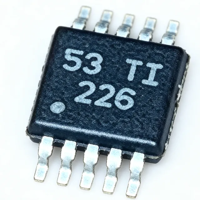
The Texas Instruments INA226AIDGSR-Q1 is an AEC-Q100 qualified, 36V, 16-bit current shunt and power monitor with an I2C- or SMBus-compatible interface, packaged in a 10-pin VSSOP (DGS). It measures both a shunt voltage drop (bidirectional, high-side or low-side) and bus supply voltage, then computes power, current, and energy with ultra-precise resolution. A current shunt and power monitor is a precision analog front-end placed across a series sense resistor; it belongs to the broader hierarchy of current sensing ICs, power management ICs, and semiconductor devices. By digitizing the microvolt-level shunt drop with a 16-bit delta-sigma ADC, it converts raw current into calibrated digital data that microcontrollers can read over I2C. Key features include a 16-bit ADC resolution for fine measurement granularity, a bus voltage monitoring range up to 36V, bidirectional shunt measurement enabling both charge and discharge tracking, a multi-function ALERT pin, and two address pins (A0, A1) supporting multiple devices on one I2C bus. Automotive AEC-Q100 qualification makes it suitable for vehicle environments. The architecture pairs a precision front-end with a programmable conversion-time and averaging engine, allowing engineers to trade conversion speed against noise performance. Register-based configuration permits calibration for specific shunt values, so current and power are reported in native units without host-side computation. Typical applications include automotive battery management systems, server and telecom power rails, solar/MPPT power monitoring, and industrial motor drive current sensing. In battery systems, the bidirectional measurement tracks both charging and discharging current through a single shunt. Design consideration: shunt resistor selection directly trades measurement resolution against power dissipation; keep the full-scale shunt drop within the input range while minimizing shunt loss at peak load.

ISM303DACTR - 3D Accel + 3D Magnetometer SiP | STMicroelectronics
The STMicroelectronics ISM303DACTR is a high-performance, low-power, compact system-in-package (SiP) that integrates a 3D digital linear acceleration sensor and a 3D digital magnetic sensor in a single 3x3x1 mm LGA-12 module. It supports user-selectable linear acceleration full scales of plus or minus 2 g, plus or minus 4 g, plus or minus 8 g, and plus or minus 16 g, with output data rates reaching 6400 Hz, while its magnetic field dynamic range extends to plus or minus 50 gauss with output data rates up to 150 Hz. Communication is provided through a digital I2C serial bus interface (with standard, fast, fast-mode-plus, and high-speed modes at 100 kHz, 400 kHz, 1 MHz, and 3.4 MHz) as well as an SPI interface, both configurable through the device pinout. A 3D accelerometer and magnetometer module is a multi-axis inertial sensor that measures linear acceleration along three orthogonal axes and the Earth's magnetic field vector along three axes. These sensors fall under the broader categories of MEMS (micro-electro-mechanical systems) sensors, inertial measurement units, and eCompass (electronic compass) building blocks, which in turn belong to the larger family of motion and position sensors used in modern electronic systems. Key features of the ISM303DACTR include an embedded low-power motion engine for tilt detection, free-fall, wake-up, single/double tap recognition, 6D/4D orientation, and pedometer functions; a programmable finite state machine for application-level event handling; and a magnetic sensor with built-in self-test, offset cancellation, and temperature compensation. Two independent interrupt lines (INT1/INT2) let the host processor stay in low-power sleep until a configurable threshold event occurs, reducing overall system energy consumption in battery-powered designs. Architecturally, the device combines a capacitive MEMS accelerometer front-end with a Hall-effect AMR magnetometer, each followed by dedicated sigma-delta ADCs, a shared I2C/SPI digital interface, and an embedded interrupt controller. Both sensors share a common 1.71 V to 3.6 V supply rail, and the digital logic operates from a separate VDDIO rail, allowing mixed-voltage designs. The integrated temperature sensor and 16-bit data output keep raw sensitivity stable across the -40 C to +85 C operating range. Typical applications for the ISM303DACTR include eCompass and tilt-compensated magnetic heading in handheld navigation, industrial tilt/inclination sensing, robotics orientation tracking, vibration monitoring in predictive maintenance, and remote/HMI control with gesture/click recognition. Its small footprint and embedded intelligence make it well suited for wearable fitness trackers, AR/VR headsets, and IoT sensor nodes. When designing with this part, allocate a 2.2 uF or larger bulk decoupling capacitor on VDD and a 100 nF X7R bypass as close to the IC pin as possible. The device is intended for reflow soldering; moisture sensitivity level MSL3 handling is required. Always run the in-built self-test at startup to verify both accelerometer and magnetometer integrity in production. This page combines XAIPART-verified distributor pricing, drop-in replacement candidates, and practical design integration notes not found in the manufacturer datasheet alone, giving buyers and design engineers a single source for sourcing decisions.

LDC3114-Q1 - 4-Ch Inductive Touch Sensor 16-TSSOP | TI
The Texas Instruments LDC3114-Q1 is a 4-channel hybrid inductive touch and inductance-to-digital converter supplied in a 16-pin TSSOP (PW) package measuring 5.00 mm x 4.40 mm. It converts changes in inductance caused by conductive target movement into digital data, enabling contactless button, slider, and proximity sensing without mechanical wear. An inductance-to-digital converter (LDC) is a specialized sensor interface IC that measures the resonant frequency shift of an LC tank driven by a conductive target. Within the sensor signal chain hierarchy, it sits between the raw coil sensor and the host MCU, functioning as both an excitation source and a digitizer. LDCs belong to the broader family of capacitive/inductive position and touch sensing interfaces used across automotive and industrial human-machine interfaces. Key features include four well-matched sensing channels that support differential and ratiometric measurements, allowing compensation of environmental and aging effects such as temperature drift and mechanical drift. The device communicates through an I2C interface for simple configuration, and an ultra-low power mode is specifically intended for power on/off buttons and position sensors in battery-powered applications. The device is AEC-Q1 qualified, making it suitable for automotive in-cabin and body electronics designs. Technically, the LDC3114-Q1 drives external coils directly and reports proximity or touch state via I2C registers, offloading threshold computation from the host processor. The well-matched channel structure improves multi-button uniformity, while the single-ended sensing method simplifies sensor PCB layout compared to differential architectures. Typical applications include automotive touch buttons on steering wheels and center consoles, contactless rotary/position sensing in knobs and dials, and industrial control panels where sealed, mechanical-free interfaces improve reliability in harsh environments. Design consideration: keep the LC tank components close to the device and follow the TI sensor PCB layout guidelines to minimize parasitic capacitance; the single-ended architecture is more EMI-sensitive than differential predecessors such as the LDC1662, so shielding and ground plane practices matter.

LDC3114QPWR - 4-Ch Inductance-to-Digital Touch Sensor | TI
The Texas Instruments LDC3114QPWR is a 4-channel hybrid inductive touch and inductance-to-digital converter (LDC) with I2C interface, housed in a 16-pin TSSOP (PW) package rated from -40C to +125C. An inductance-to-digital converter is a sensor interface IC that measures the impedance shift of an external LC tank circuit - typically a copper coil or PCB trace inductor paired with a capacitor - and converts that shift into a digital value. Within the sensor-signal-conditioning hierarchy (sensor AFE -> inductive sensing IC -> sensor interface -> mixed-signal IC), an LDC translates physical events such as a finger press, metal target movement, or spring compression into register data that a microcontroller reads over I2C. Key features include 4 independent sensing channels for multi-button touch panels or position sensing, an ultra-low power mode for battery-powered power on/off buttons, and simple configuration through the I2C interface. The device integrates the excitation and demodulation circuitry internally, so designers only add an external coil and capacitor per channel, reducing bill-of-materials complexity compared with capacitive sensing that requires specialized electrodes. Technically, the LDC3114 drives each channel's LC tank, monitors resonant impedance, and outputs raw and processed data registers; internal compensation and button-detection algorithms offload the host MCU. The hybrid architecture supports both inductive touch buttons and continuous inductance measurement for linear or rotary position sensing. Typical applications include waterproof or gloved-touch buttons on appliances and industrial panels, metal-target proximity switches, and linear or rotary position sensing in knobs and sliders. The TSSOP-16 package suits compact control boards. Design consideration: choose the external capacitor to set the resonant frequency within the datasheet-supported range, and keep sensor coils away from ground planes to maximize sensitivity. This page synthesizes distributor pricing, drop-in alternatives, and practical design notes not found in the manufacturer datasheet.

LIS2DE12TR - 3-Axis MEMS Accelerometer, 2g/4g/8g/16g | STMicroelectronics
The STMicroelectronics LIS2DE12TR is a low-power, 3-axis linear accelerometer with a digital I2C/SPI serial interface, designed for a wide range of motion-sensing applications. It features user-selectable full-scale ranges of ±2g, ±4g, ±8g, and ±16g, and supports output data rates from 1 Hz to 5.3 kHz. The device operates from a 1.71V to 3.6V supply and is available in a compact 12-lead LGA package (2x2x1 mm), making it ideal for space-constrained portable and wearable designs. An accelerometer is a sensor that measures proper acceleration (the rate of change of velocity) of a body in its own instantaneous rest frame. In the context of MEMS (Micro-Electro-Mechanical Systems), accelerometers typically use capacitive sensing elements to detect changes in capacitance caused by the displacement of a proof mass under acceleration. The LIS2DE12TR belongs to the category of motion sensors, which are a subset of sensors used in electronic systems to detect movement, orientation, and vibration. Motion sensors play a critical role in applications ranging from consumer electronics (smartphones, wearables) to industrial monitoring and automotive safety systems. Key features of the LIS2DE12TR include an ultra-low-power consumption of 2 µA in low-power mode at 10 Hz ODR, a 16-bit data output, and an embedded first-in, first-out (FIFO) buffer that reduces host processor load. The device also integrates a programmable interrupt generator for motion detection, free-fall detection, and 6D/4D orientation detection, enabling always-on functionality with minimal power draw. The I2C and SPI interfaces provide flexibility for system integration, and the device is RoHS compliant and halogen-free. From a technical perspective, the LIS2DE12TR uses a capacitive sensing element with a dedicated ASIC (Application-Specific Integrated Circuit) for signal conditioning and digital conversion. The device includes a self-test capability that allows verification of the sensing element and electronics, and it operates over a temperature range of -40°C to +85°C. The LGA package is designed for surface-mount assembly and is compatible with standard reflow soldering processes, with a moisture sensitivity level (MSL) of 1. Typical applications include motion-activated user interfaces, orientation detection in portable devices, vibration monitoring in industrial equipment, and activity tracking in wearables. The low power consumption and small footprint make it particularly suitable for battery-powered IoT devices and smart home sensors. When designing with the LIS2DE12TR, ensure proper decoupling of the power supply with a 100 nF capacitor placed close to the VDD pin, and route the I2C/SPI lines with appropriate pull-up resistors. The interrupt pins can be configured to wake the host processor only when motion is detected, significantly extending battery life in always-on applications.
LIS2DH12TR - 3-Axis Accelerometer, ±2/±4/±8/±16g | STMicroelectronics
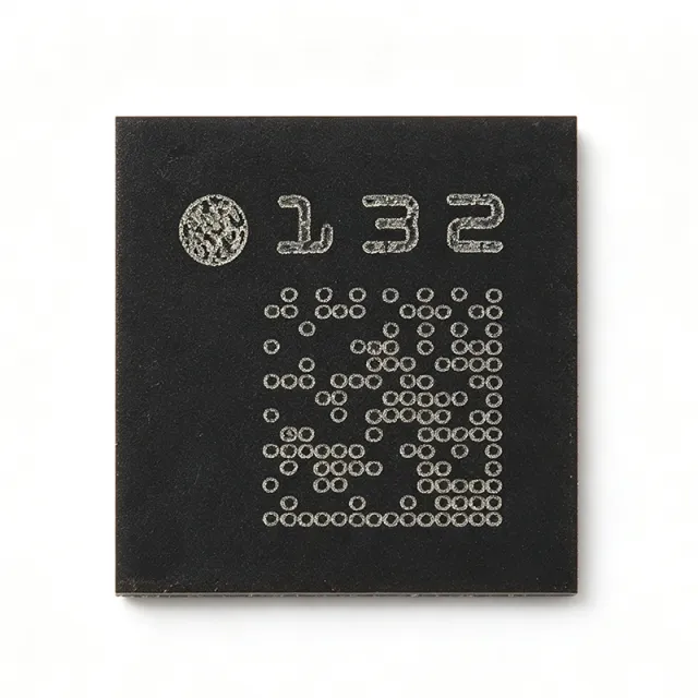
The STMicroelectronics LIS2DH12TR is a 3-axis linear accelerometer with a digital I2C/SPI serial interface, offering user-selectable full-scale ranges of ±2g, ±4g, ±8g, and ±16g. It is housed in a compact 12-lead LGA package (2x2x1 mm) and operates from a 1.71V to 3.6V supply, making it ideal for battery-powered and space-constrained applications. Data verified as of 2026-08-05. An accelerometer is a sensor that measures proper acceleration (g-force) along one or more axes. The LIS2DH12 is a MEMS (Micro-Electro-Mechanical Systems) capacitive accelerometer, which detects changes in capacitance caused by the displacement of a proof mass under acceleration. In the system hierarchy, it is a motion sensor -> inertial sensor -> MEMS sensor -> sensor, and it is commonly used in motion-activated functions, orientation detection, and vibration monitoring. Key features include a wide full-scale range selection, a 16-bit data output, an embedded 32-level FIFO buffer, and a built-in high-pass filter. The device supports multiple operating modes (normal, low-power, and high-resolution) with output data rates from 1 Hz to 5.3 kHz. It also includes a self-test capability and an interrupt generator for motion detection, enabling low-power always-on applications. The LIS2DH12 uses a capacitive sensing element and a dedicated IC interface, achieving low noise (220 µg/√Hz in high-resolution mode) and low power consumption (as low as 2 µA in low-power mode at 1 Hz ODR). The digital output simplifies system integration, eliminating the need for external ADCs. The device is AEC-Q100 qualified for automotive applications, ensuring reliability in harsh environments. Typical applications include mobile devices for screen rotation and step counting, industrial vibration monitoring, and automotive anti-theft systems. Its low power and small footprint make it suitable for wearable devices and IoT sensors. In a smartphone, the LIS2DH12 detects orientation to switch between portrait and landscape modes, and it can count steps by analyzing acceleration patterns. When designing with this device, ensure proper decoupling of the power supply with a 100 nF capacitor close to the VDD pin. The I2C address is selectable via the SA0 pin, allowing multiple devices on the same bus. For battery-powered designs, use the low-power mode to extend battery life, and configure the FIFO to reduce host processor wake-ups. This page synthesizes distributor pricing, drop-in alternatives, and practical design notes not found in the ST datasheet, providing a comprehensive resource for engineers evaluating the LIS2DH12TR.
LIS2DU12TR - Ultra-Low-Power 3-Axis Accelerometer, ±16g, I2C/SPI | STMicroelectronics
The STMicroelectronics LIS2DU12TR is an ultra-low-power, high-performance 3-axis linear accelerometer housed in a 12-pin LGA package (2.0 x 2.0 x 0.7 mm). The LIS2DU12TR supports user-selectable full scales of ±2g, ±4g, ±8g, and ±16g, with output data rates programmable from 1.6 Hz up to 800 Hz, and it embeds an analog antialiasing filter ahead of the ADC to relax external filter requirements. An accelerometer is a MEMS sensor that measures linear acceleration along one or more axes and converts it into an electrical signal; the LIS2DU12 is a three-axis digital accelerometer whose MEMS structure and ASIC were co-designed to deliver low noise and ultra-low current consumption. It belongs to the broader hierarchy of inertial sensors -> MEMS accelerometers -> motion sensors -> semiconductor components, and integrates high-level digital features such as a 128-level FIFO buffer, motion and free-fall detection, and a programmable interrupt generator that reduces host wake-ups. Key features of the LIS2DU12TR include selectable resolution (8/10/12-bit, low-power modes), an embedded temperature sensor, and primary digital interfaces consisting of I2C/SPI (with MIPI I3C-compatible modes) and an auxiliary SPI for OIS or second-sensor pairing. Power consumption reaches sub-µA levels in the dedicated low-power modes, while one-shot and wake-up paths allow always-on operation in battery-powered designs. The supply range spans 1.62 V to 3.6 V and an independent VDDIO rail supports 1.8 V / 3.3 V mixed-voltage hosts. The MEMS die uses a high-aspect-ratio capacitive sensing element whose deflection is read by a low-noise charge-sharing front end; on-chip digital processing performs offset, gain, and self-test calibration, and the integrated antialiasing filter suppresses out-of-band energy before data-rate decimation. An extended self-test routine checks the full signal path at every startup or on demand from the system controller. Typical applications include wearable fitness bands, asset trackers, hearables and TWS earbuds, IoT vibration and tap detectors, smart-home security, handheld medical motion monitors, and always-on industrial tilt and free-fall sensors for logistics or hard-disk protection. Stacked with a magnetometer, it also serves as a 9-DoF IMU building block for portable navigation. When designing with the LIS2DU12TR, place the device near a mechanically stiff region of the PCB, keep high-current traces away from the LGA, and follow the datasheet decoupling guidance (typically 0.1 µF + bulk on VDD and VDDIO). The wide range of FIFO and interrupt modes allows most use cases to be handled in event-driven firmware without continuous polling, dramatically reducing system power consumption. This page synthesizes distributor pricing, drop-in pin-compatible alternatives, and practical design notes not found in the manufacturer datasheet alone.
LIS2DUX12TR - Ultra-Low Power AI Accelerometer | 12-LGA (2x2)
The STMicroelectronics LIS2DUX12TR is an ultra-low-power, smart, digital 3-axis linear accelerometer (MEMS + ASIC) housed in a 12-pin LGA (2x2 mm) package, with user-selectable full scales of ±2g, ±4g, ±8g, and ±16g and an output data rate range of 0.8 Hz to 400 Hz. A MEMS accelerometer is a micro-electro-mechanical sensor that measures linear acceleration along one or more axes; the LIS2DUX12 belongs to the smart-accelerometer category (MEMS sensor -> accelerometer -> inertial sensor -> motion sensor) and adds always-on intelligence through an on-chip finite state machine (FSM) and machine learning core (MLC) with adaptive self-configuration (ASC), offloading always-on gesture and vibration classification entirely to the sensor. Key features include ultra-low current consumption designed for always-on battery-powered applications, an integrated anti-aliasing filter to simplify signal conditioning, ±2g/±4g/±8g/±16g selectable full scale, a 0.8 Hz to 400 Hz output data rate range, and a MIPI I3C slave interface for fast, low-pin-count digital communication. The device also integrates a 128-level FIFO buffer that lets the host processor stay in deep sleep between event bursts, an embedded temperature sensor, and an embedded self-test routine. The 12-LGA 2x2 mm package has an exposed pad for thermal dissipation and mechanical stress relief. The LIS2DUX12 combines a low-noise MEMS sensing element with a digital ASIC implementing the I3C/I2C/SPI interface, an anti-aliasing stage, the FSM/MLC classifiers, and the FIFO. The anti-aliasing filter is implemented in the digital domain to reduce the external analog component bill of materials while maintaining clean spectral output for motion and vibration analysis. Typical applications include wearable fitness bands, hearables, TWS earbuds, asset tracking, smartphone motion UI, industrial vibration monitoring, and IoT gesture interfaces. The always-on FSM/MLC allows event detection at nanowatt or single-digit microwatt average power, extending coin-cell battery life into months or years. Design considerations include a clean 1.8V supply to the VDD pin and a separate VDDIO rail for the digital I/O domain, decoupling capacitors placed as close as possible to the supply pins, and a PCB footprint with a central thermal/ground pad soldered to a board ground plane to minimize mechanical stress on the package. This page synthesizes distributor pricing, drop-in alternatives, and practical design notes not found in the manufacturer datasheet, including side-by-side comparisons with the Bosch Sensortec BMA456 and BMA253.
LIS2HH12TR - 3-Axis Accelerometer, ±2/±4/±8g | STMicroelectronics
The STMicroelectronics LIS2HH12TR is a high-performance 3-axis linear accelerometer with digital I2C/SPI output, designed for a wide range of motion-sensing applications. It features user-selectable full-scale ranges of ±2g, ±4g, and ±8g, with a resolution of 16-bit data output. The device operates from a 1.71V to 3.6V supply voltage and is available in a compact 12-lead LGA package (2x2x1 mm), making it ideal for space-constrained designs. An accelerometer is a sensor that measures proper acceleration, which is the rate of change of velocity per unit time. In the context of motion sensing, accelerometers detect linear acceleration along one or more axes, enabling applications such as orientation detection, vibration monitoring, and free-fall detection. The LIS2HH12TR is a MEMS (Micro-Electro-Mechanical Systems) capacitive accelerometer, which uses microscopic mechanical structures to sense acceleration-induced capacitance changes. As a member of the accelerometer family, it falls under the broader category of inertial sensors, which also includes gyroscopes and magnetometers. In a typical system hierarchy, the LIS2HH12TR serves as a motion sensor within the sensor subsystem, feeding data to a microcontroller or application processor via I2C or SPI. Key features of the LIS2HH12TR include a low power consumption of 180 µA in normal mode, a wide supply voltage range of 1.71V to 3.6V, and a high-resolution 16-bit output. The device also integrates a 32-level FIFO buffer, which reduces host processor load by storing acceleration data for batch retrieval. Additionally, it includes an embedded temperature sensor and supports a wide operating temperature range of -40°C to +85°C. The LIS2HH12TR is RoHS compliant and halogen-free, meeting modern environmental standards. Technically, the LIS2HH12TR utilizes a capacitive sensing element with a dedicated ASIC for signal conditioning and digital conversion. The device offers a noise density of 220 µg/√Hz, ensuring accurate measurements in low-vibration environments. It supports both I2C (up to 400 kHz) and SPI (up to 10 MHz) interfaces, providing flexibility in system integration. The built-in self-test feature allows for functional verification during production, enhancing reliability. The device also includes programmable interrupt generators for motion detection, enabling event-driven wake-up and sleep modes. Typical applications include portable and wearable devices, IoT nodes, industrial condition monitoring, and automotive anti-theft systems. In portable devices, the LIS2HH12TR enables screen rotation and step counting, while in industrial settings, it monitors machinery vibration for predictive maintenance. Its low power consumption makes it suitable for battery-powered IoT sensors that require long operational life. When designing with the LIS2HH12TR, ensure proper decoupling of the power supply with a 100 nF capacitor placed close to the VDD pin. The I2C address is selectable via the SA0 pin, allowing multiple devices on the same bus. For optimal performance, avoid mechanical stress on the LGA package during PCB assembly, and follow the recommended land pattern provided in the datasheet.
LIS2MDLTR - 3-Axis Digital Magnetometer | STMicroelectronics | IoT & Navigation
The STMicroelectronics LIS2MDLTR is a 3-axis digital magnetometer that measures magnetic field strength with high resolution and low power consumption. It operates from a 1.71V to 3.6V supply voltage and communicates via I2C or SPI interfaces, making it suitable for a wide range of consumer, industrial, and IoT applications. The device is housed in a compact 12-pin LGA package (2.0 x 2.0 x 0.7 mm), enabling space-constrained designs. A magnetometer is a sensor that measures the strength and direction of magnetic fields. In the context of electronic systems, a 3-axis magnetometer detects the Earth's magnetic field to determine orientation relative to magnetic north, functioning as an electronic compass. It is often combined with accelerometers and gyroscopes in inertial measurement units (IMUs) to provide full orientation tracking. The LIS2MDLTR belongs to the category of magnetic field sensors, which are part of the broader sensor family used in navigation, robotics, and consumer electronics. Key features of the LIS2MDLTR include a wide magnetic field range of ±50 gauss, a selectable output data rate from 10 Hz to 100 Hz, and a 16-bit resolution that provides fine granularity for precise heading calculations. The device also features an embedded temperature sensor, a programmable interrupt generator, and a self-test capability. Its low power consumption, with a typical current draw of 0.6 mA in normal mode and 1 µA in power-down mode, extends battery life in portable devices. The LIS2MDLTR uses a magneto-resistive sensing element that changes resistance in response to magnetic fields, processed by an integrated analog-to-digital converter (ADC) and digital signal processing chain. The device includes a FIFO buffer to store measurement data, reducing host processor wake-up frequency. The I2C interface supports up to 400 kHz, while the SPI interface operates up to 10 MHz, providing flexibility for various system architectures. Typical applications include smartphone compasses, navigation systems, augmented reality devices, and industrial position sensing. In a smartphone, the LIS2MDLTR provides heading information for map orientation and location-based services. In industrial settings, it can detect the presence and orientation of magnetic components in automated assembly lines. The device's small footprint and low power make it ideal for wearable devices and IoT nodes. When designing with the LIS2MDLTR, ensure proper PCB layout to minimize magnetic interference from nearby traces and components. Place the sensor away from ferrous materials and current-carrying conductors. The device supports both I2C and SPI, so select the interface that best fits the system's communication architecture. Calibration is recommended to compensate for hard-iron and soft-iron effects in the final product.

LIS344ALHTR - 3-Axis ±2/±6g Analog MEMS Accelerometer | STMicroelectronics
The STMicroelectronics LIS344ALHTR is a 3-axis analog-output MEMS linear accelerometer with user-selectable ±2g or ±6g full-scale range, supplied in a 16-lead LGA (4 mm × 4 mm) package. The device operates from a single 2.4 V to 3.6 V supply, draws 0.65 mA typical current, and provides three ratiometric analog voltage outputs (X, Y, Z) through a 1.8 kHz mechanical sensor bandwidth. An accelerometer is an inertial sensor that measures proper acceleration along one or more axes. Capacitive MEMS accelerometers use a suspended proof-mass whose displacement unbalances a differential capacitor; demodulation electronics then produce an analog output voltage proportional to acceleration. The LIS344ALH belongs to the family of low-power, signal-conditioned linear accelerometers used in consumer and industrial motion-sensing applications. Key features include ratiometric analog outputs whose offset and sensitivity scale with the supply voltage, embedded self-test capability, and 10,000 g shock survivability. Typical noise floor is 190 µg/√Hz, enabling detection of small tilt or vibration signals. The wide supply range (2.4 V – 3.6 V) and low current consumption (~0.65 mA at 3 V) suit portable, battery-powered designs. Architecturally, the LIS344ALHTR combines a three-axis capacitive sensing element with a CMOS signal-conditioning ASIC. Outputs are buffered and ratiometric, simplifying ADC interfacing by eliminating the need for a precise reference. The user-selectable ±2 g / ±6 g full-scale range is set via a logic-level FS pin, allowing one part to serve both high-g and low-g applications. Embedded self-test verifies mechanical and electronic integrity without external fixtures. Typical applications include tilt and inclination sensing in handheld devices, motion-activated user interfaces, vibration monitoring in industrial equipment, free-fall detection for hard-disk protection, robotics posture estimation, and gaming peripherals. The 1.8 kHz mechanical bandwidth also supports platform-stabilization loops and structural-vibration logging. When designing with this part, place 100 nF decoupling capacitors close to the supply pin, route output traces over a continuous ground plane to minimize noise pickup, and use a clean low-impedance 3V3 regulator. Use the self-test feature at power-up to detect mechanical damage on the proof mass. This page synthesizes distributor pricing, drop-in alternatives, and practical design notes not found in the manufacturer datasheet, delivering actionable sourcing and selection data alongside the verified specifications.

LIS3DHTR - 3-Axis Ultra-Low-Power Accelerometer | STMicroelectronics
The LIS3DHTR is an ultra-low-power, high-performance three-axis linear accelerometer from STMicroelectronics, part of the 'nano' family. It features a digital I2C/SPI serial interface and is available in a compact 16-lead LGA package (3x3 mm). The device supports selectable full-scale ranges of ±2g, ±4g, ±8g, and ±16g, with output data rates from 0.5 Hz to 625 Hz. It operates over a supply voltage range of 1.71V to 3.6V and a temperature range of -40°C to +85°C. An accelerometer is a sensor that measures proper acceleration, which is the rate of change of velocity per unit time. In the context of MEMS (Micro-Electro-Mechanical Systems), accelerometers are used to detect motion, tilt, vibration, and shock. The LIS3DHTR belongs to the category of digital-output accelerometers, which integrate sensing elements with signal conditioning and an analog-to-digital converter, providing digital data directly to a host microcontroller. This makes it a key component in motion-sensing systems, from consumer electronics to industrial monitoring. Key features of the LIS3DHTR include an ultra-low-power consumption of 2 µA in low-power mode, a 32-level FIFO buffer to reduce host processor intervention, and an embedded temperature sensor. It also offers motion detection, free-fall detection, and 6D/4D orientation detection. The device supports both I2C and SPI interfaces, with a wide range of programmable interrupt outputs for event-driven applications. Technically, the LIS3DHTR uses a capacitive sensing element with a dedicated ASIC for signal processing. It provides 16-bit data output, with a resolution of 1 mg per LSB at ±2g range. The device includes a self-test capability and is factory-calibrated. Its low power consumption and small footprint make it ideal for battery-powered portable devices. Typical applications include mobile phones, wearable devices, gaming controllers, and IoT sensors. In these applications, the LIS3DHTR enables features such as screen rotation, step counting, gesture recognition, and fall detection. Its high resolution and low noise ensure accurate motion tracking. When designing with the LIS3DHTR, ensure proper decoupling of the power supply with a 100 nF capacitor close to the VDD pin. The I2C address is selectable via the SA0 pin, allowing multiple devices on the same bus. For optimal performance, place the sensor away from high-frequency noise sources and follow the layout guidelines in the datasheet.
LIS3MDLTR - 3-Axis Digital Magnetometer | STMicroelectronics
The LIS3MDLTR is a 3-axis digital magnetometer from STMicroelectronics, designed for high-resolution magnetic field sensing in a compact 12-pin LGA package. It measures magnetic fields with a full-scale range selectable from ±4 gauss to ±16 gauss, and offers a resolution of up to 0.14 mG/LSB in the ±4 gauss range. The device communicates via both I2C and SPI interfaces, making it versatile for integration into a wide range of systems. A magnetometer is a sensor that measures the strength and direction of magnetic fields. In the context of consumer electronics and IoT, magnetometers are often used as electronic compasses to determine orientation relative to Earth's magnetic field. They are part of the broader category of motion and orientation sensors, which also includes accelerometers and gyroscopes. The LIS3MDLTR specifically provides a digital output, simplifying interface with microcontrollers and eliminating the need for external analog-to-digital converters. Key features of the LIS3MDLTR include a wide supply voltage range of 1.9V to 3.6V, low power consumption with a typical current of 0.45 mA in high-resolution mode, and a selectable output data rate from 0.625 Hz to 1000 Hz. The device also includes an embedded temperature sensor, a programmable interrupt generator, and a self-test capability. These features enable precise magnetic field measurement while maintaining low power for battery-operated devices. The LIS3MDLTR uses a MEMS (Micro-Electro-Mechanical Systems) technology with a magneto-resistive sensing element, providing high sensitivity and stability. The device includes a signal conditioning chain with an ADC, a digital filter, and a FIFO buffer to reduce host processor load. The I2C address is 0x1E (default) and can be configured via the SA0 pin. The SPI interface supports both 3-wire and 4-wire modes, offering flexibility in system design. Typical applications include electronic compasses in smartphones and wearables, navigation systems, magnetic field mapping, and industrial position sensing. The LIS3MDLTR is also used in augmented reality (AR) and virtual reality (VR) headsets for head tracking, and in robotics for orientation detection. Its low power and small footprint make it ideal for portable and space-constrained designs. When designing with the LIS3MDLTR, ensure proper PCB layout to minimize magnetic interference from nearby traces and components. Place the sensor away from ferrous materials and high-current paths. Use decoupling capacitors on the power supply pins and follow the recommended layout in the datasheet for optimal performance.

LM235 - Precision Temperature Sensor | STMicroelectronics | Industrial
The LM235 is a precision integrated-circuit temperature sensor that produces an output voltage linearly proportional to the Celsius temperature. It operates over a temperature range of -40°C to +125°C and provides an output of 10 mV/°C with a typical accuracy of ±1°C at 25°C. The device is available in a TO-92 package, making it suitable for through-hole mounting in a wide range of applications. A temperature sensor is a device that converts thermal energy into an electrical signal, typically a voltage or current, that can be measured and processed. The LM235 belongs to the family of analog temperature sensors, which are widely used in environmental monitoring, industrial control, and consumer electronics. These sensors are essential in systems that require temperature compensation, thermal protection, or precise temperature measurement. Key features of the LM235 include a wide operating voltage range of 4V to 30V, low self-heating of 0.1°C in still air, and a linear output of 10 mV/°C. The device also features a typical accuracy of ±1°C at 25°C and ±2°C over the full temperature range. Its low output impedance and ability to drive capacitive loads make it easy to interface with analog-to-digital converters (ADCs) and microcontrollers. The LM235 uses a bandgap reference circuit to generate a voltage proportional to temperature, ensuring stable and repeatable performance. The output voltage is calibrated at the factory, eliminating the need for external trimming in most applications. The device operates from a single supply and can be used in both single-ended and differential configurations. Typical applications include temperature monitoring in industrial process control, thermal management in power supplies, battery temperature sensing in portable devices, and environmental monitoring in HVAC systems. The LM235 is also used in automotive applications for engine temperature sensing and cabin climate control. When designing with the LM235, ensure that the supply voltage is within the specified range and that the output is properly buffered if driving a low-impedance load. The device's low self-heating minimizes measurement errors, but for high-accuracy applications, consider using a heat sink or mounting the sensor away from heat sources.

LM26CIM5X-YPE/NOPB - ±3°C Factory Preset Thermostat | Texas Instruments
The LM26CIM5X-YPE/NOPB is a precision, single digital-output, low-power thermostat from Texas Instruments, part of the LM26 family. It integrates an internal reference, DAC, temperature sensor, and comparator in a compact SOT-23-5 (DBV) package. This device features a factory-preset trip point of 115°C and provides an active-low, open-drain digital output, making it ideal for over-temperature protection in a wide range of systems. Operating from a 2.7V to 5.5V supply, it draws minimal quiescent current, ensuring low power consumption in battery-powered applications. A thermostat is a temperature switch that triggers a digital output when the temperature crosses a preset threshold. The LM26 is a solid-state thermostat, meaning it uses semiconductor sensing rather than mechanical contacts, offering higher reliability and faster response. It belongs to the temperature sensor hierarchy: thermostat -> temperature switch -> temperature sensor -> sensor -> electronic component. This device is specifically the LM26NV variant, which omits the analog VTEMP output, focusing solely on digital trip functionality. Key features include ±3°C accuracy over the full operating range, a fixed trip point of 115°C, and an active-low open-drain output that can sink current to drive external loads or interface with logic. The device also includes a built-in hysteresis of 10°C (typical) to prevent output oscillation. The SOT-23-5 package is lead-free and RoHS compliant, suitable for surface-mount assembly. Technically, the LM26 uses a bandgap reference and a DAC to set the trip point, with a comparator that monitors the temperature sensor output. The open-drain output requires an external pull-up resistor, typically 10kΩ, to define the logic-high level. The device operates over a temperature range of -55°C to 125°C, making it suitable for harsh environments. Its low supply current of 40µA (typical) ensures minimal thermal self-heating, preserving accuracy. Typical applications include over-temperature protection for power supplies, battery chargers, motor controllers, and industrial equipment. The 115°C trip point is well-suited for protecting components that must not exceed this temperature, such as power transistors and voltage regulators. The small footprint and low cost make it ideal for high-volume consumer and automotive electronics. When designing with this device, ensure the open-drain output is properly pulled up and that the supply voltage is decoupled with a 0.1µF ceramic capacitor close to the V+ pin. The thermal path to the PCB should be optimized to ensure accurate sensing of the target component's temperature.