Sensoren
Unterkategorien
Produkte (525)

LM63CIMA - Remote Diode Temp Sensor & Fan Control | TI SOIC-8
The Texas Instruments LM63CIMA is a ±1°C/±3°C accurate remote diode digital temperature sensor with integrated PWM fan control, housed in an 8-pin SOIC package. It accurately measures its own die temperature (local channel) and the temperature of a diode-connected transistor such as a 2N3904 or the thermal diode commonly embedded in CPUs, GPUs, and ASICs (remote channel), with a measurement range of 0°C to 125°C and a supply range of 3.0V to 3.6V. The SMBus/2-wire compatible interface delivers 8-bit (sign + 10-bit) signed temperature data and exposes tachometer input plus PWM fan-control output. A remote diode digital temperature sensor is a class of thermal-management IC that converts the temperature-dependent Vbe of a small-signal transistor into a digital reading via an on-chip ADC. In the broader power-management hierarchy these ICs sit alongside fan drivers, hot-swap controllers, and hardware monitors, enabling closed-loop thermal regulation in systems where overheating degrades reliability. Unlike thermistors or thermocouples, remote-diode sensors provide noise-immune digital output and factory-trimmed calibration, which simplifies firmware development on the chip. Key features include ±1°C local accuracy and ±3°C remote accuracy (typical), factory-calibrated series-resistance correction, a 10-bit-plus-sign remote-diode temperature ADC with 0.25°C LSB resolution, a TACH input for closed-loop fan-speed feedback, and a PWM output whose duty-cycle to support both low-frequency and high-frequency fans. The device also integrates a digital over-temperature alarm with ALERT pin interrupt, an SMBus ALERT-response address, and an offset register for system-level error trimming. The 8-pin SOIC (DIMA) package and SMBus interface allow direct drop-in upgrade of legacy LM63 designs. Architecturally, the LM63 uses a delta-Vbe sensing front-end, an integrating ADC with chopper-stabilized offset cancellation, and a state machine that handles SMBus transactions and PWM pulse-width calculation in hardware. The remote channel supports series-resistance cancellation up to a few hundred ohms of trace resistance, allowing flexible PCB routing between the IC and the sense diode. An on-chip digital filter suppresses spurious readings caused by PWM edge noise. Typical applications include processor and chipset thermal monitoring in desktop and server motherboards, graphics-card GPU thermal management, embedded-system fan-speed control, set-top-boxed and projector lamp-cooling control, and industrial chassis-temperature regulation. Designers can create boards based on TI's LM63 EVM reference schematic, which shows the recommended 2N3904 diode-connection topology, bypass-cap placement, and PWM low-pass network. When designing with this device, place the 0.1 µF VDD bypass capacitor within a few millimeters of the supply pin and use a 10 kΩ NTC bypass resistor at the D+/D- pins when the diode is omitted. Program the PWM output frequency to match the fan's tachometer gearing, and use the ALERT instruction to drive an interrupt for hot-swap events.
LM63CIMA/NOPB - Remote Diode Temp Sensor with Fan Control | Texas Instruments
The Texas Instruments LM63CIMA/NOPB is a digital temperature sensor with integrated fan control, housed in an 8-pin SOIC (D) package. It features a 2-wire SMBus serial interface, measures its own die temperature (0°C to +125°C) plus an external remote diode temperature with ±1°C accuracy, and provides a PWM output for direct fan-speed regulation. A remote-diode digital temperature sensor is a device that converts the base-emitter junction voltage of a thermally-coupled transistor or diode-connected semiconductor into a digital temperature reading. Within the broader sensor hierarchy, this places the LM63 in the category of digital thermal monitoring ICs used in power management and thermal management subsystems of PCs, servers, graphics cards, and embedded SoCs. By combining both a local and a remote channel into a single IC, the part eliminates the need for a separate thermistor circuit, reducing BOM cost and PCB area while improving measurement accuracy. Key features include ±1°C remote-diode accuracy (factory trimmed for series-resistance cancellation when paired with a 2N3904 NPN or processor substrate diode), ±3°C local sensor accuracy, 8-bit plus sign-bit resolution (0.5°C/LSB), and a programmable PWM output whose duty cycle is derived from the remote-channel temperature. The 2-wire SMBus interface operates up to 400 kHz and supports SMbus alert (SMBALERT) and T_CRIT/T_HIGH limits for hardware-controlled shutdown. The LM63 integrates a Sigma-Delta ADC front-end optimized for diode Vbe measurements, and includes TruTherm technology that compensates for series resistance between the sensor and the thermal diode. The output PWM frequency is user-selectable (programmed via SMBus), enabling compatibility with 3-wire and 4-wire fan implementations. Operating from 3.0 V to 3.6 V, the device typically consumes 1.1 mA in active conversion and offers a low-current standby mode. Typical applications include CPU/GPU thermal management on desktops, workstations, and embedded single-board computers; ASIC/FPGA chassis monitoring; and industrial-grade fan-speed control loops. The remote diode can be tied directly to a substrate thermal diode embedded in modern processors, graphics chips, or ASICs, providing accurate core-temperature reporting without discrete thermistors. When designing with this part, place the remote-diode traces as a differential pair with ground guarding to reject noise, and keep the trace length short to minimize measurement error. Verify fan drive polarity and the input range of your fan before connecting the PWM output directly to a fan tach pin.
LM63CIMAX - ±1°C Remote Diode Temp Sensor + Fan Control | TI
The Texas Instruments LM63CIMAX is a ±1°C/±3°C accurate remote-diode digital temperature sensor with integrated fan control, housed in an 8-pin SOIC (MAX) package. It measures its own internal die temperature plus the junction temperature of a remote diode-connected transistor (such as a 2N3904 or the substrate diode of a CPU/GPU/ASIC) and drives a PWM output to control a cooling fan based on programmable trip thresholds. A remote-diode temperature sensor is a class of thermal management IC that exploits the temperature-dependent base-emitter voltage of a bipolar or substrate diode to infer junction temperature far away from the sensor itself. Remote-diode sensors sit within the thermal management IC hierarchy (PMIC > thermal management > temperature sensor > remote-diode sensor) and are essential in desktop PCs, servers, and any system where a hot spot must be monitored without placing the sensor physically on the heat source. Key specifications include ±1°C remote-diode accuracy (0°C to +125°C) and ±3°C accuracy from 0°C to +85°C, 8-/10-bit-plus-sign internal/remote resolution, a 2-wire SMBus (I²C-compatible) digital interface, and a programmable PWM fan-control output with tachometer input for closed-loop RPM feedback. Supply voltage is 3.0V to 3.6V and quiescent current is roughly 1.3 mA during active conversion. The LM63CIMAX integrates a sigma-delta ADC for noise rejection, on-chip offset trim performed at the factory to minimize diode non-ideality errors, and a tachometer counter that reports fan RPM over the SMBus. The MAX package exposes a single remote-diode differential input pair (D+/D−) and the fan-driver PWM output (Fan Out), plus the digital interface pins (SDA, SCL, ALERT, GND, VDD, FAN_IN/TACH). Typical applications include CPU/GPU thermal monitoring in desktop and server motherboards, fan-speed control in telecom equipment, and chassis-intake temperature sensing in industrial controllers. The integrated fan tachometer input enables closed-loop RPM regulation rather than open-loop PWM drive, which reduces acoustic noise and extends fan life. When designing with the LM63CIMAX, keep the D+/D− routing balanced, length-matched, and surrounded by ground to cancel noise pickup that would otherwise appear as temperature noise. Decouple VDD close to the IC with a 0.1 µF ceramic capacitor and avoid routing the remote-diode traces near switching fan-drive signals to preserve accuracy.
LM63CIMAX/NOPB - SMBus Temp Sensor and Fan Controller
The Texas Instruments LM63CIMAX/NOPB is an active remote-diode digital temperature sensor with integrated fan control, local temperature sensing, and a 2-wire SMBus output in an 8-pin SOIC package. The verified manufacturer and distributor data identify the device as a fan-control and temperature-monitor IC covering 0°C to 125°C, with one remote diode temperature channel and one local temperature channel. Its remote sensing capability supports diode-connected transistors such as a 2N3904 or thermal diodes found in processors, GPUs, and other ASICs. The LM63 combines monitoring and fan-control functions, reducing the need for separate temperature sensors and fan-control logic in compact thermal-management systems. A remote-diode temperature sensor uses a semiconductor junction as a temperature-sensitive element. The LM63 measures both a remote junction and its own local temperature, then makes digital measurements available through the SMBus interface. This makes the device part of the temperature-sensor and thermal-management IC hierarchy, rather than a general-purpose analog sensor. The integrated fan-control section is intended to compare measured temperature with programmable thresholds and manage cooling in systems such as desktop computers, industrial electronics, and embedded processors. Key verified characteristics include an 8-SOIC package, a 0°C to 125°C advertised monitoring range, internal and external sensing channels, and 2-wire SMBus communication. The manufacturer describes the LM63 as factory-trimmed for series accuracy, while the exact remote-diode accuracy, fan-control thresholds, SMBus address, and electrical limits were not included in the supplied verified excerpts. Those missing values are intentionally not inferred. LCSC lists a starting price of $5.0093 as of 2026-10-08, and DigiKey and Mouser provide product, inventory, and pricing resources for current sourcing. The LM63 is appropriate when a design needs remote junction monitoring and direct fan-control integration in one device. It is especially relevant to processor, GPU, ASIC, and other high-density electronic systems where a local thermal diode is available. Compared with a simple temperature sensor, the LM63 adds fan-control functionality and SMBus digital communication. Compared with a discrete thermal-control implementation, it can reduce component count and simplify firmware access to temperature data. Designers should verify the exact package pinout, operating-voltage limits, SMBus addressing, remote-diode connection method, fan-drive ratings, and thermal accuracy against the current Texas Instruments datasheet before layout release. The remote diode should be placed close to the intended thermal region, with routing designed to minimize heat conduction and measurement error. This page synthesizes verified distributor listings, manufacturer descriptions, and design guidance without inventing missing electrical parameters.

LM75ADP - Digital Temp Sensor & Thermal Watchdog | NXP
The NXP Semiconductors LM75ADP is a digital temperature sensor and thermal watchdog with an on-chip bandgap temperature sensor and Sigma-Delta A-to-D conversion technique. Housed in an 8-pin TSSOP (SOT505-1) package, the LM75A is a pin-for-pin upgrade of the legacy LM75 with 11-bit temperature resolution (0.125 °C LSB) and operates from a single 2.8 V to 5.5 V supply. A digital temperature sensor is an IC that converts on-die thermal energy into a binary word readable by a host processor over a serial bus (typically I²C). Within the broader hierarchy, the LM75ADP sits in the sensor chain as a local-only device (no remote diode), beneath which fall thermistors, RTDs and analog temperature sensors. It functions as a thermal management building block at the board level, alongside fan controllers and supervisory circuits. The LM75A's headline features include ±2 °C accuracy over the -55 °C to +125 °C range, an I²C/SMBus-compatible interface with three selectable address pins (allowing up to eight devices on one bus), and a programmable OVERTEMP output that asserts when the measured temperature crosses a user-defined threshold. The device also integrates a configurable hysteresis register to prevent chatter around the trip point, and offers both a normal mode for periodic monitoring and a shutdown mode that drops supply current below 10 µA. Internally, the architecture pairs a precision bandgap reference with a Sigma-Delta modulator; the modulator's 1-bit stream is filtered by a decimation filter to produce the 11-bit signed result (8-bit integer plus 3-bit fraction). The OVERTEMP pin is implemented as an open-drain comparator output with the trip level and hysteresis both stored in on-chip registers, which lets the host configure thermal-window alarming in software rather than with external analog parts. Typical applications include PC/embedded system thermal monitoring, industrial controller over-temperature protection, battery-pack charge management, LCD/projector overheat shutdown, and any HVAC-style closed-loop where a low-cost, low-pin-count digital sensor is preferred over a thermistor plus ADC. Because the LM75ADP is industry-standard LM75 register-compatible, it is a frequent retrofit into LM75 sockets where higher resolution is required without firmware changes. When designing with the LM75A, observe I²C pull-up sizing: the open-drain SDA/SCL lines must be pulled to VCC through 4.7 kΩ resistors on a 3.3 V bus; the OVERTEMP pin also requires an external pull-up because it is open-drain. Decouple VCC with a 100 nF ceramic capacitor placed within 5 mm of the supply pin. This page synthesizes distributor pricing, drop-in alternatives sourced from the NXP/ADT75/TI cross-references, and practical design notes not collected in any single manufacturer datasheet.
LM75AIMX/NOPB - ±2°C Digital Temp Sensor & Thermal Watchdog, I2C, SOIC-8 | Texas Instruments
The Texas Instruments LM75AIMX/NOPB is an industry-standard digital temperature sensor and thermal watchdog with a 2-wire I2C/SMBus-compatible interface, housed in an 8-pin SOIC (D) package. It features a local temperature sensing range of -55°C to +125°C with ±2°C accuracy (max) and 9-bit (0.5°C LSB) resolution, supplied from a 2.7V to 5.5V rail. The on-chip delta-sigma ADC, bandgap reference, and over-temperature interrupt (O.S. output) make it a self-contained thermal management building block. A digital temperature sensor such as the LM75A is a mixed-signal IC that combines an on-die thermal diode, sigma-delta ADC, calibration registers, and a digital serial interface to report die temperature in a standard two's-complement format. Within the broader component taxonomy, the LM75A belongs to the local temperature sensor family, which sits under analog/mixed-signal sensors, under sensors, and ultimately under semiconductors. Compared with thermistors, the LM75A eliminates linearization math, PCB real estate, and ADC channel overhead; compared with remote-diode sensors, the LM75A sacrifices baseboard hot-spot accuracy for BOM simplicity. Key features include 9-bit (0.5°C LSB) signed two's complement output, user-programmable 9-bit O.S. (overtemperature shutdown) and Hysteresis registers, a fault-queue counter to suppress false triggers, and three selectable I2C address pins (A0/A1/A2) that allow up to eight LM75A devices on a single bus. Standby current is just 1 µA typical, and the O.S. output is an open-drain interrupt that can wire-OR multiple devices. Technically, the LM75A uses a thin-film on-die thermal element whose forward voltage is sampled by a chopper-stabilized delta-sigma ADC against an internal bandgap reference; the digital value is then stored in the 16-bit temperature register (high byte + sign/low byte). The SMBus-compatible interface supports standard (100 kHz), fast (400 kHz), and high-speed (3.4 MHz) modes, and the part includes power-on reset and a configurable hardware shutdown mode for battery-powered designs. Typical applications include base-station equipment thermal monitoring, server and desktop PC system protection, office electronics (printers, copiers), portable battery packs, HVAC controllers, and any thermistor-replacement design. The combination of 2.7V operation, SMBus compatibility, and eight selectable addresses makes it especially attractive for multi-zone chassis monitoring in networking and industrial control. When designing with the LM75A, place the part at the actual thermal hot spot of the board and provide a low-impedance ground pour, since the die temperature is what is reported rather than ambient air. A 0.1 µF decoupling capacitor within 5 mm of VDD is recommended, and pull-up resistors on SDA, SCL, and O.S. must be sized to the bus capacitance and the chosen I2C speed. This page synthesizes current distributor pricing, drop-in replacement options, and practical PCB layout guidance not assembled in the manufacturer datasheet alone.

LM75BIMM-5/NOPB - ±2°C I2C Temp Sensor, 3V-5.5V | TI
The Texas Instruments LM75BIMM-5/NOPB is a ±2°C accuracy digital local temperature sensor with an integrated Delta-Sigma analog-to-digital converter and I2C/SMBus-compatible two-wire interface, housed in an 8-pin VSSOP (DGK) package. It operates from 3.0 V to 5.5 V, delivers 9-bit temperature data with 0.5°C resolution, and supports a measurement range of -55°C to +125°C. The device combines a bandgap reference, oversampling ADC, and a programmable over-temperature alarm with hardware OS output. A digital temperature sensor is an integrated circuit that converts on-chip thermal conditions into a calibrated digital word readable by a microcontroller. Compared with discrete NTC thermistors or RTDs, they integrate the sensor, signal conditioning, ADC, and a serial interface on one die, eliminating calibration, linearization, and external ADC circuitry. The LM75B sits inside the hierarchy: temperature sensor -> sensor IC -> analog/mixed-signal semiconductor - in short, a self-contained thermal data source for embedded systems. Key features include a factory-calibrated accuracy of ±2°C across the full -55°C to +125°C range, 0.5°C resolution (9-bit signed), a dedicated OS (overtemperature shutdown) open-drain alert pin for interrupt or comparator-style system response, and three address-select pins (A0-A2) that allow up to eight devices on a single I2C bus. Power consumption is rated at 1 mA active and 4 uA shutdown current, and the part is rated for -55°C to +125°C operation with shutdown current of 4 uA per the manufacturer datasheet. The LM75B uses a bandgap-temperature proportional core feeding a Sigma-Delta modulator to generate the digital code, achieving noise as low as 0.125°C over the 20 Hz to 100 kHz bandwidth while eliminating the need for external signal conditioning. The OS comparator and polarity-programmable INT/CMP_TSTAT pin allow hardware-based thermal protection without host intervention, reducing firmware overhead in safety-critical designs. Typical applications include thermal management in computing platforms and 1U/2U servers, system over-temperature protection in industrial controllers, portable battery-powered consumer electronics, cold-junction compensation in thermistor/RTD circuits, and general embedded system health monitoring. Designers value its ability to deliver calibrated digital data directly to a microcontroller or BMC over a two-wire bus. When designing with the LM75B, place the VSSOP-8 package close to the heat source (such as a power stage or SoC) and connect the OS pin to the host interrupt or shutdown controller for failsafe behavior. Decouple the supply with a 100 nF ceramic capacitor placed within 5 mm of the VDD pin to meet I2C noise immunity requirements. This page synthesizes distributor pricing, drop-in alternatives, and practical design notes not found in the manufacturer datasheet.

LMT84LPM - 1.5V 10uA Analog Temp Sensor TO-92 | TI
The Texas Instruments LMT84LPM is a precision CMOS analog output temperature sensor in a TO-92-3 through-hole package, covering -50C to +150C with a linear output of -5.5 mV/C that is inversely proportional to temperature. It operates from a supply as low as 1.5V while drawing only 5.4 uA quiescent current, making it one of the lowest-power analog temperature sensors available. An analog temperature sensor converts local temperature into a proportional voltage that a microcontroller ADC or comparator can read directly, without digital bus configuration. Within the signal chain hierarchy, it sits alongside thermistors and RTDs as a sensing element, but the LMT84 family replaces passive thermistors with a calibrated, linear, push-pull (Class-AB) output that drives heavy loads without an external buffer. Key features include +/-0.4C typical accuracy (+/-2.7C maximum), 1.5V minimum supply for single-cell battery operation, 0.7 ms power-on time enabling aggressive power-cycling, and Class-AB source/sink output capability. The inverse transfer function also provides inherent failsafe behavior: a shorted output reads as maximum temperature, which systems can detect. Architecturally, the LMT84 uses a CMOS bandgap-derived sensing core with a Class-AB output stage, giving strong output drive in both directions and low sensitivity to supply noise compared with thermistor divider circuits. Typical applications include battery-powered sensing nodes, automotive climate and battery-pack monitoring (via the AEC-Q100 Grade 0 qualified LMT84-Q1 variant), appliance and HVAC thermal protection, and portable medical devices. Design tip: because output swing is negative-sloped, remember ADC code decreases with rising temperature; at 30C the output is approximately 537 mV per the datasheet lookup table.

LMT84LPM - 1.5V Analog Temperature Sensor TO-92 | TI
The Texas Instruments LMT84LPM is a precision CMOS analog output temperature sensor in a TO-92-3 package, operating from a supply as low as 1.5V with only 5.4 uA quiescent current. It delivers a linear analog output voltage inversely proportional to temperature at a gain of -5.5 mV per degree C, spanning -50C to +150C. An analog output temperature sensor is a type of temperature sensor IC (part of the broader sensor and semiconductor hierarchy) that converts measured die temperature directly into a proportional voltage, which a microcontroller ADC can read without digital bus configuration. Unlike thermistors, analog sensors provide a linear, calibrated transfer function; unlike digital sensors such as the TMP117, they require no I2C/SMBus protocol stack. Key features include 1.5V-capable single-supply operation, 10 uA-class current consumption for effective power-cycling in battery-powered designs, a Class-AB push-pull output capable of sourcing and sinking heavy loads, 0.7 ms power-on time, and typical accuracy of plus or minus 0.4C (plus or minus 2.7C maximum) per the TI LMT84 datasheet. Architecturally, the LMT84 uses a CMOS bandgap-derived temperature-dependent voltage with an output stage that maintains linearity across the full -50C to +150C range while drawing micropower supply current, enabling years of operation from a small lithium cell. Typical applications include battery-powered environmental monitoring, HVAC thermal sensing, portable medical devices, automotive sub-systems (via the AEC-Q100 qualified LMT84-Q1 variant), and appliance over-temperature detection. Design tip: because output gain is negative (-5.5 mV/C), invert the transfer function in firmware; add a 0.1 uF bypass capacitor close to the supply pin for stable ADC readings.
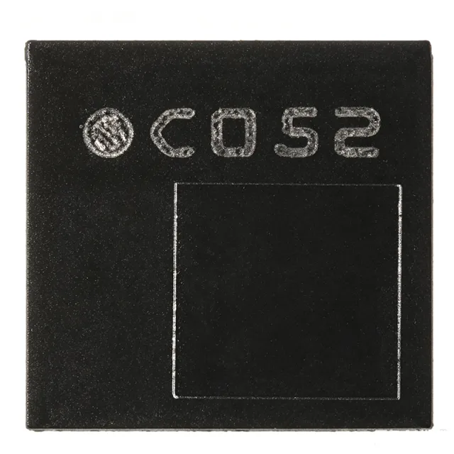
LPS22HBTR - MEMS Pressure Sensor, 260-1260 hPa | STMicroelectronics
The STMicroelectronics LPS22HBTR is a MEMS capacitive absolute pressure sensor with a digital I2C/SPI interface, offering a measurement range of 260 to 1260 hPa (absolute) with high accuracy and low power consumption. It is housed in a compact 2.0 x 2.0 x 0.7 mm HLGA package, making it suitable for space-constrained portable and wearable devices. A pressure sensor is a device that measures the force exerted by a fluid (liquid or gas) per unit area, converting this physical quantity into an electrical signal. The LPS22HBTR is a MEMS (Micro-Electro-Mechanical Systems) capacitive pressure sensor, which uses a thin diaphragm that deflects under pressure, changing the capacitance between the diaphragm and a fixed electrode. This change is then converted into a digital output via an integrated signal conditioner. Pressure sensors are a subset of environmental sensors, which also include temperature, humidity, and gas sensors, and are essential components in IoT, automotive, and industrial systems. Key features of the LPS22HBTR include an absolute pressure range of 260 to 1260 hPa, a resolution of 0.01 hPa (8 Pa), and an accuracy of ±0.1 hPa (typical) at 25°C. The device operates from a supply voltage of 1.7V to 3.6V, with a current consumption of 12 µA at 1 Hz output data rate (ODR) and 1 µA in power-down mode. It supports both I2C (up to 400 kHz) and SPI (up to 10 MHz) interfaces, and includes an integrated 24-bit ADC, a 128-level FIFO, and an interrupt output for data-ready and pressure threshold events. The LPS22HBTR is built using ST's proven MEMS technology, which ensures high reliability and long-term stability. The device includes a temperature sensor for compensation, and its output is factory-calibrated, eliminating the need for user calibration. The HLGA package is designed for surface-mount assembly and is RoHS and halogen-free compliant. Typical applications include barometric altimeters in drones and smartphones, weather stations, GPS dead-reckoning for navigation, and indoor navigation systems. Its low power consumption and small footprint make it ideal for battery-powered IoT devices and wearables. When designing with the LPS22HBTR, ensure proper PCB layout with a small pressure port opening to the environment, and avoid covering the sensing element with solder mask or conformal coating. The device's I2C address is 0x5C (7-bit) or 0xB8 (8-bit), and it can be configured via its registers for different ODRs and interrupt modes.
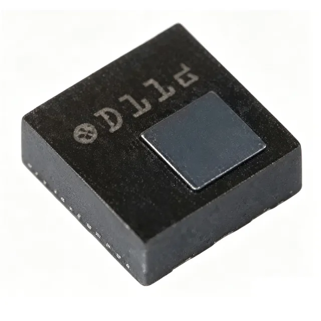
LPS22HH - MEMS Pressure Sensor, 260-1260 hPa | STMicroelectronics
The STMicroelectronics LPS22HH is a MEMS capacitive absolute pressure sensor with a digital I2C and SPI interface, offering a measurement range of 260 to 1260 hPa. It is housed in a compact 2.0 x 2.0 x 0.7 mm HLGA package, making it suitable for space-constrained applications. A pressure sensor is a device that measures the force exerted by a fluid (liquid or gas) per unit area, converting it into an electrical signal. The LPS22HH is an absolute pressure sensor, meaning it measures pressure relative to a perfect vacuum. It belongs to the family of MEMS (Micro-Electro-Mechanical Systems) sensors, which integrate mechanical and electrical components on a microscopic scale. In the broader hierarchy, it is a pressure sensor -> MEMS sensor -> sensor -> electronic component, commonly used in environmental monitoring and altitude sensing. Key features include an absolute pressure range of 260 to 1260 hPa, a resolution of 0.02 hPa (RMS), and an accuracy of ±0.1 hPa (typical) at 25°C. The sensor operates from a supply voltage of 1.7V to 3.6V, with a low power consumption of 12 µA at 1 Hz output data rate. It supports output data rates from 1 Hz to 200 Hz, and includes an integrated temperature sensor with ±0.5°C accuracy. The device is RoHS compliant and operates over a temperature range of -40°C to +85°C. The LPS22HH uses a capacitive sensing element with a precision analog front-end and a 24-bit sigma-delta ADC, providing high-resolution digital output. The sensor includes a FIFO buffer (up to 100 samples) to reduce host processor load, and supports interrupt generation for data-ready and threshold events. The I2C address is 0x5C (default) or 0x5D (alternate), selectable via the SA0 pin. Typical applications include barometric altimeters in drones and wearables, weather stations, and indoor navigation systems. Its low power and small size make it ideal for battery-powered IoT devices. The sensor is also used in smartphone and smartwatch for elevation tracking and stair climbing detection. When designing with the LPS22HH, ensure proper PCB layout with a small vent hole to expose the sensing element to ambient pressure. Avoid placing the sensor near heat sources to minimize temperature-induced errors. Use the built-in FIFO to reduce I2C/SPI traffic and power consumption in low-power applications.

LPS22HII - MEMS Nano Pressure Sensor, 260-1260 hPa | STMicroelectronics
The STMicroelectronics LPS22HII is an ultra-compact piezoresistive absolute pressure sensor functioning as a digital output barometer. It measures pressure in the range of 260 to 1260 hPa with an absolute accuracy of 0.5 hPa, making it suitable for altimetry and weather station applications. The sensor is housed in a 10-pin LGA package (2.0 x 2.0 x 0.7 mm) and communicates via I2C or SPI interfaces. A pressure sensor is a device that converts applied pressure into an electrical signal. The LPS22HII is a MEMS (Micro-Electro-Mechanical Systems) pressure sensor, which uses a thin silicon membrane that deflects under pressure, changing the piezoresistive elements' resistance. This change is converted into a digital output via an integrated ADC. Pressure sensors are a subset of environmental sensors, which also include temperature, humidity, and gas sensors. In the sensor hierarchy, the LPS22HII is a barometric pressure sensor, a type of absolute pressure sensor, and a MEMS sensor. Key features include a 24-bit pressure data output, an embedded temperature sensor, and a 16-bit temperature output. The sensor supports data rates from 1 Hz to 75 Hz, with a typical current consumption of 12 uA at 1 Hz output data rate. It operates from a 1.7V to 3.6V supply voltage, making it suitable for battery-powered devices. The LPS22HII also includes a FIFO buffer, interrupt pins, and a pressure threshold detection feature. The LPS22HII uses a MEMS capacitive sensing element with a signal conditioning ASIC, providing high accuracy and low power consumption. The sensor has a pressure noise of 0.0075 hPa RMS, enabling precise measurements. It is designed for portable devices, with a small footprint and low height, and is compatible with lead-free soldering processes. Typical applications include altimeters in drones and smartphones, weather station barometers, and GPS dead-reckoning for navigation. The sensor's low power and small size make it ideal for wearable devices and IoT nodes. In a drone, the LPS22HII provides altitude data for flight stabilization and landing. When designing with the LPS22HII, ensure proper PCB layout with a pressure port opening for accurate readings. The sensor should be placed away from heat sources to minimize temperature-induced errors. Use the FIFO to reduce host processor wake-ups and save power.

LPS25HBTR - MEMS Pressure Sensor, 260-1260 hPa | STMicroelectronics
The STMicroelectronics LPS25HBTR is a piezoresistive absolute pressure sensor with a digital I2C/SPI interface, designed for high-resolution measurement of barometric pressure and temperature. It operates over a pressure range of 260 to 1260 hPa (absolute) and a temperature range of -40°C to +85°C, making it suitable for a wide variety of environmental and industrial applications. The sensor is housed in a compact 2.0 x 2.0 x 0.7 mm LGA-8 package, enabling integration into space-constrained designs. A MEMS pressure sensor is a micro-electromechanical system that converts applied pressure into an electrical signal. The LPS25HBTR uses a piezoresistive sensing element whose resistance changes with mechanical stress induced by pressure. This change is converted into a digital output via an internal analog-to-digital converter (ADC) and signal conditioning circuitry. The sensor belongs to the broader category of environmental sensors, which also includes temperature, humidity, and gas sensors, and is a key component in IoT, weather monitoring, and altitude sensing systems. Key features of the LPS25HBTR include an absolute pressure range of 260 to 1260 hPa, a resolution of 0.01 hPa (equivalent to approximately 8 cm of altitude change), and a typical accuracy of ±0.1 hPa over the full range. The device supports both I2C (up to 400 kHz) and SPI (up to 10 MHz) interfaces, with a selectable address for I2C. It also includes an embedded 24-bit ADC, a 32-level FIFO buffer, and an interrupt output for data-ready and threshold detection. The supply voltage ranges from 1.7V to 3.6V, with a low current consumption of 4 µA in normal mode and 1 µA in low-power mode. The LPS25HBTR integrates a temperature sensor with an accuracy of ±0.5°C, which can be used for temperature compensation of the pressure reading or as a standalone temperature measurement. The device features a pressure resolution of 0.01 hPa and a temperature resolution of 0.01°C. The FIFO buffer allows the host processor to remain in low-power mode while the sensor collects data, reducing overall system power consumption. The interrupt pin can be configured to trigger on pressure thresholds or data-ready events, enabling event-driven operation. Typical applications include barometric pressure sensing for weather stations, altitude measurement in drones and smartphones, indoor navigation, and industrial process control. The sensor's high resolution and low power make it ideal for battery-powered IoT devices. In a drone application, the LPS25HBTR provides altitude data with an accuracy of ±0.1 hPa, which translates to approximately ±0.8 meters, enabling stable flight control. When designing with the LPS25HBTR, ensure proper PCB layout with a small vent hole or port to expose the sensing element to ambient pressure. Avoid placing the sensor near heat sources, as temperature gradients can affect pressure readings. Use a low-pass filter on the power supply to reduce noise, and follow the recommended layout in the datasheet for optimal performance.
LPS27HHW - MEMS Pressure Sensor, 260-1260 hPa | STMicroelectronics
The STMicroelectronics LPS27HHW is a high-resolution MEMS pressure sensor with an absolute pressure range of 260 to 1260 hPa and an embedded temperature sensor. It communicates via I2C or SPI and is housed in a compact 2.0 x 2.0 x 0.7 mm LGA package, making it suitable for portable and space-constrained applications. A MEMS pressure sensor is a micro-electromechanical system that measures absolute or gauge pressure by detecting the deflection of a thin silicon membrane. The LPS27HHW belongs to the category of barometric pressure sensors, which are used to measure atmospheric pressure and altitude. In the broader system hierarchy, it is a sensor component within the larger category of environmental sensors, which also include temperature, humidity, and gas sensors. These sensors are essential in applications such as weather stations, drones, and smartphones for altitude and navigation. Key features of the LPS27HHW include a pressure sensing range of 260 to 1260 hPa, an absolute pressure accuracy of ±0.1 hPa, and a temperature accuracy of ±0.5 °C. The device supports both I2C and SPI interfaces, with I2C addresses 0x5C and 0x5D selectable via the SA0 pin. It operates from a supply voltage of 1.7 V to 3.6 V, with a low power consumption of 4 µA at 1 Hz output data rate. The sensor also features a 24-bit pressure output and a 16-bit temperature output, providing high resolution for precise measurements. The LPS27HHW is built on ST's proven MEMS technology, which ensures high reliability and long-term stability. The device includes an internal signal conditioning chain, an analog-to-digital converter, and a digital interface, all integrated into a single chip. The sensor's low noise and high resolution make it ideal for applications requiring accurate pressure and altitude measurements, such as drone altitude hold, smartphone barometer, and weather station monitoring. Typical applications include drone altitude control, where the sensor provides precise altitude data for stable flight; smartphone barometer for indoor navigation and weather forecasting; and industrial pressure monitoring for HVAC systems. The sensor's small footprint and low power consumption make it suitable for battery-powered devices. When designing with the LPS27HHW, ensure proper PCB layout with a small vent hole to expose the pressure port to the environment. Avoid placing the sensor near heat sources or in direct airflow to minimize measurement errors. The I2C pull-up resistors should be sized appropriately for the bus speed and capacitance.

LPS33HW - MEMS Pressure Sensor, 260-1260 hPa | STMicroelectronics
The STMicroelectronics LPS33HW is a high-resolution MEMS pressure sensor with an absolute pressure range of 260 to 1260 hPa and an embedded temperature sensor. It is housed in a compact 2.0 x 2.0 x 0.76 mm ceramic LGA package (CCLGA-10L) and communicates via I2C or SPI interfaces. The device operates from a 1.7V to 3.6V supply and features a 24-bit pressure output, achieving a typical RMS pressure noise of 0.008 hPa (at 1 Hz output data rate). A MEMS pressure sensor is a micro-electromechanical system that measures absolute or gauge pressure by detecting the deflection of a thin silicon diaphragm. The LPS33HW belongs to the family of barometric pressure sensors, which are essential in altimetry, weather monitoring, and indoor navigation. In the broader system hierarchy, it is a sensor component within the category of environmental sensors, feeding data to microcontrollers for processing and decision-making. Key features include a pressure sensing range of 260 to 1260 hPa, a resolution of 0.008 hPa, and an embedded temperature sensor with an accuracy of ±0.5°C. The device supports both I2C (up to 400 kHz) and SPI (up to 10 MHz) interfaces, and includes a 128-level FIFO buffer to reduce host processor load. It also features an interrupt pin for data-ready and pressure threshold events, and a low-power mode with a current consumption of 3 µA at 1 Hz output data rate. The LPS33HW is built on ST's proven MEMS technology, which ensures high stability and low drift over temperature and time. The ceramic LGA package provides excellent thermal and mechanical robustness, making it suitable for harsh environments. The device includes an internal temperature compensation algorithm, which maintains accuracy across the full operating temperature range of -40°C to +85°C. Typical applications include barometric altimeters in drones and wearables, weather station modules, indoor navigation and floor detection in smartphones, and industrial pressure monitoring. Its low power consumption and small footprint make it ideal for battery-powered IoT devices. When designing with the LPS33HW, ensure proper PCB layout with a small vent hole to expose the pressure port to ambient air, and avoid covering the port with solder mask or conformal coating. Decouple the supply pins with a 100 nF capacitor placed close to the device.
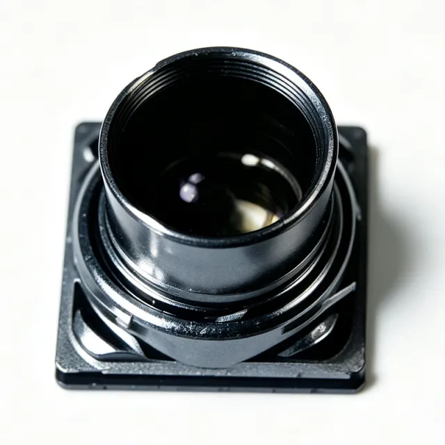
LPS33HWTR - MEMS Pressure Sensor, 260-1260 hPa | STMicroelectronics
The STMicroelectronics LPS33HWTR is a high-resolution MEMS pressure sensor with an absolute pressure range of 260 to 1260 hPa, designed for barometric and altimetry applications. It integrates a sensing element and an I2C/SPI interface in a compact 3 mm x 3 mm x 1.7 mm LGA package, enabling precise atmospheric pressure measurement with a typical accuracy of ±0.1 hPa. A MEMS pressure sensor is a micro-electromechanical system that converts applied pressure into an electrical signal, typically through a deformable diaphragm whose deflection is measured capacitively or piezoresistively. In the system hierarchy, a MEMS pressure sensor is a type of pressure sensor, which falls under the broader category of sensors, and ultimately within the domain of microelectronics and IoT devices. The LPS33HWTR specifically uses a capacitive sensing element with a signal-conditioning ASIC, providing digital output via I2C or SPI. Key features include a 24-bit resolution, an output data rate (ODR) from 1 Hz to 75 Hz, and an embedded temperature sensor. The device operates from a 1.7V to 3.6V supply, with a low power consumption of 4 µA at 1 Hz ODR. It also features a FIFO buffer, interrupt pins for data-ready and pressure threshold detection, and a built-in pressure and temperature compensation. The LGA package is designed for surface-mount assembly, with a footprint compatible with standard reflow soldering. Technically, the LPS33HWTR employs a MEMS capacitive pressure cell that changes capacitance with applied pressure. The ASIC converts this capacitance change into a digital pressure value using a 24-bit ADC, with internal compensation for temperature and supply variations. The device supports both I2C (up to 400 kHz) and SPI (up to 10 MHz) interfaces, allowing flexible integration with microcontrollers. The FIFO buffer can store up to 32 samples, reducing host processor load. Typical applications include barometers for weather stations, altimeters for drones and wearables, and pressure monitoring in industrial and medical devices. Its high accuracy and low power make it suitable for battery-powered IoT devices, where it can be used for altitude tracking or environmental monitoring. The device also finds use in smartphone and smartwatch applications for indoor navigation and activity tracking. When designing with the LPS33HWTR, ensure proper PCB layout with a small vent hole for pressure access, and avoid covering the sensing port with solder mask. The device requires a decoupling capacitor (100 nF) close to the VDD pin, and the I2C/SPI lines should be kept short to minimize noise. For best accuracy, calibrate the sensor at a known pressure and temperature, and consider the effect of altitude on pressure readings.

LSM303AGRTR - 3D Accelerometer & Magnetometer | STMicroelectronics
The STMicroelectronics LSM303AGRTR is an ultra-low-power, high-performance 3-axis accelerometer and 3-axis magnetometer combined into a single system-in-package. It is designed for consumer and industrial motion sensing applications, offering a digital output via I2C and SPI interfaces. The device operates from a 1.71V to 3.6V supply voltage and features a wide measurement range for both acceleration (±2g, ±4g, ±8g, ±16g) and magnetic field (±50 gauss). The LSM303AGRTR is housed in a compact 2mm x 2mm x 1mm LGA-12 package, making it ideal for space-constrained designs. An accelerometer is a sensor that measures proper acceleration, which is the rate of change of velocity of a body in its own instantaneous rest frame. In the context of motion sensing, accelerometers are used to detect tilt, vibration, and shock. A magnetometer measures the strength and direction of magnetic fields, commonly used for compass applications and detecting magnetic anomalies. The LSM303AGRTR combines both sensors in one package, enabling applications such as orientation detection, navigation, and gesture recognition. This integration reduces board space and simplifies design compared to using separate accelerometer and magnetometer components. Key features of the LSM303AGRTR include a 16-bit resolution for both accelerometer and magnetometer, a programmable interrupt system, and a built-in temperature sensor. The accelerometer offers selectable full-scale ranges of ±2g, ±4g, ±8g, and ±16g, while the magnetometer provides a range of ±50 gauss. The device supports both I2C and SPI communication, with I2C addresses 0x19 and 0x1E for the accelerometer and magnetometer respectively. The LSM303AGRTR also features a FIFO buffer for data storage, reducing host processor load, and an embedded self-test capability for functional verification. The LSM303AGRTR is fabricated using a proprietary micromachining process that integrates the sensing elements and signal conditioning circuitry on a single chip. The accelerometer uses a capacitive sensing principle, while the magnetometer uses a magneto-resistive principle. The device includes a 16-bit ADC for each channel, ensuring high-resolution measurements. The low power consumption, with typical current draw of 180 µA in normal mode and 2 µA in power-down mode, makes it suitable for battery-powered applications. The device also includes a smart power management system that automatically switches between power modes based on data rate and activity. Typical applications for the LSM303AGRTR include mobile phones and tablets for screen rotation and gaming, wearable devices for step counting and activity tracking, and IoT devices for motion-based control. It is also used in robotics for orientation and navigation, and in industrial equipment for vibration monitoring. The combination of accelerometer and magnetometer enables accurate heading and tilt compensation in compass applications, which is critical for navigation systems. When designing with the LSM303AGRTR, it is important to consider the placement of the sensor to avoid magnetic interference from nearby components such as speakers or motors. The device should be placed away from ferromagnetic materials and high-current traces. Additionally, proper decoupling capacitors (100 nF) should be placed close to the VDD and VDD_IO pins to ensure stable operation. The I2C pull-up resistors should be sized appropriately for the bus capacitance and speed.

LSM303DTR - 3D Accelerometer + Magnetometer | STMicroelectronics
The LSM303DTR is a system-in-package featuring a 3D digital linear acceleration sensor and a 3D digital magnetic sensor, manufactured by STMicroelectronics. It combines a 3-axis accelerometer and a 3-axis magnetometer in a single LGA-16 (3x3x1mm) package, providing a complete 6-axis motion sensing solution. The device communicates via I2C or SPI interfaces, with a wide supply voltage range of 2.16V to 3.6V, making it suitable for battery-powered portable applications. A 3D accelerometer is a sensor that measures linear acceleration along three perpendicular axes (X, Y, Z), typically used to detect motion, tilt, and vibration. A 3D magnetometer measures the strength and direction of the magnetic field, functioning as an electronic compass. When combined, they form an inertial measurement unit (IMU) capable of providing orientation and heading information. The LSM303DTR integrates both sensors in a single package, reducing board space and simplifying design compared to discrete solutions. Key features include a full-scale acceleration range selectable from ±2g to ±16g, and a magnetic field full-scale range from ±2 gauss to ±12 gauss. The accelerometer offers a 16-bit data output with a noise density of 220 µg/√Hz, while the magnetometer provides 16-bit resolution with a sensitivity of 0.080 µT/LSB at ±4 gauss range. The device supports output data rates from 3.125 Hz to 1600 Hz for the accelerometer and 0.625 Hz to 100 Hz for the magnetometer, with an embedded FIFO buffer to reduce host processor load. The LSM303DTR utilizes a MEMS (Micro-Electro-Mechanical Systems) capacitive sensing element for the accelerometer and a Hall-effect or magneto-resistive sensing element for the magnetometer. The integrated signal conditioning, ADC, and digital interface eliminate the need for external components, simplifying PCB design. The device operates over a temperature range of -40°C to +85°C, making it suitable for industrial and consumer applications. Typical applications include orientation and motion sensing in smartphones, tablets, gaming controllers, and wearable devices. It is also used in robotics for tilt compensation, in navigation systems for dead reckoning, and in industrial equipment for vibration monitoring. The low power consumption, with a typical current of 2 mA in normal mode, extends battery life in portable devices. When designing with the LSM303DTR, ensure proper decoupling with a 100 nF capacitor on the power supply pins and place the sensor away from magnetic interference sources such as speakers and motors. The I2C address is 0x1E (7-bit) and can be configured via the SA0 pin. For optimal performance, follow the layout guidelines in the datasheet to minimize mechanical stress on the package.

LSM6DS3HTR - 3D Accelerometer & 3D Gyroscope iNEMO IMU | STMicroelectronics
The LSM6DS3HTR is a high-performance 3D digital accelerometer and 3D digital gyroscope system-in-package (SiP) from STMicroelectronics, designed for consumer and industrial motion sensing applications. It integrates a 3-axis accelerometer and a 3-axis gyroscope in a single 2.5 mm x 3 mm x 0.83 mm LGA-14 package, offering a compact solution for space-constrained designs. The device features a full-scale acceleration range of ±2/±4/±8/±16 g and an angular rate range of ±125/±245/±500/±1000/±2000 dps, with a 16-bit data output for both sensors. It operates from a 1.71 V to 3.6 V supply voltage and includes an advanced digital motion engine (DMP) for low-power motion processing. An inertial measurement unit (IMU) is a device that combines accelerometers and gyroscopes to measure linear acceleration and angular velocity, enabling orientation and motion tracking. IMUs are fundamental components in motion sensing systems, providing data for applications such as gesture recognition, dead reckoning, and stabilization. The LSM6DS3HTR belongs to the category of motion sensors, which are part of the broader sensor family used in IoT, wearable, and automotive systems. Its integration of both sensors in one package reduces board space and simplifies design compared to discrete solutions. Key features of the LSM6DS3HTR include a low power consumption of 0.9 mA in normal mode and 0.45 mA in low-power mode, making it suitable for battery-powered devices. It offers a 4 KB FIFO buffer to store sensor data, reducing host processor wake-up time. The device supports I2C and SPI interfaces, with a maximum I2C clock of 400 kHz and SPI clock of 10 MHz. It also includes an embedded temperature sensor, programmable interrupts, and a 6D orientation detection feature. The LGA-14 package is lead-free and RoHS compliant, with an operating temperature range of -40°C to +85°C. Technically, the LSM6DS3HTR uses a MEMS (Micro-Electro-Mechanical Systems) capacitive sensing element for both accelerometer and gyroscope, with a dedicated ASIC for signal conditioning and digital output. The device features a 16-bit ADC for each channel, providing high resolution and low noise. The embedded DMP offloads motion processing from the host, enabling features like step counting and tilt detection without host intervention. The device also includes a programmable finite state machine (FSM) for advanced motion recognition, such as activity classification. Typical applications include wearable devices (fitness trackers, smartwatches), smartphones for screen rotation and gaming, IoT nodes for motion-based wake-up, and industrial equipment for vibration monitoring. Its low power and small size make it ideal for battery-operated devices, while the high resolution and wide range support precise motion tracking in robotics and drones. When designing with the LSM6DS3HTR, ensure proper decoupling of the power supply with a 100 nF capacitor close to the VDD pin, and route the I2C/SPI lines with minimal parasitic capacitance. The device's interrupt pins can be configured to wake the host only when motion is detected, saving power. For optimal performance, place the sensor away from high-frequency noise sources and follow the layout guidelines in the datasheet.
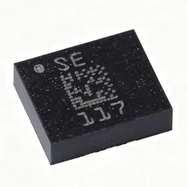
LSM6DS3TR - 3D Accelerometer & Gyroscope | STMicroelectronics
The LSM6DS3TR is a system-in-package featuring a 3D digital accelerometer and a 3D digital gyroscope from STMicroelectronics, designed for high-performance motion sensing in consumer and industrial applications. It operates from a 1.71V to 3.6V supply voltage and communicates via I2C or SPI interfaces, with a selectable full-scale range of ±2/±4/±8/±16 g for acceleration and ±125/±245/±500/±1000/±2000 dps for angular rate. The device is housed in a compact 14-lead LGA package (2.5 x 3.0 x 0.83 mm), enabling space-constrained designs. Data verified as of 2026-08-05. An inertial measurement unit (IMU) is a sensor that combines an accelerometer and a gyroscope to measure linear acceleration and angular velocity, respectively. The LSM6DS3TR integrates both sensors in a single package, providing a complete motion-sensing solution. In the system hierarchy, an IMU is a type of motion sensor, which falls under the broader category of sensors, and ultimately within the domain of microelectromechanical systems (MEMS). This integration reduces board space, simplifies design, and improves reliability compared to discrete solutions. Key features include a 16-bit data output for both accelerometer and gyroscope, an embedded 9kB FIFO for data buffering, and advanced motion detection functions such as free-fall, wake-up, single/double-tap, and 6D/4D orientation detection. The device also features a programmable interrupt generator, an embedded temperature sensor, and a low-power mode with a typical current consumption of 0.9 mA in normal mode and 1.25 mA in high-performance mode. The LSM6DS3TR supports a wide operating temperature range of -40°C to +85°C, making it suitable for harsh environments. Technically, the LSM6DS3TR utilizes a MEMS capacitive sensing element for both acceleration and angular rate, with a dedicated ASIC for signal conditioning and digital conversion. The device includes a smart FIFO that can be configured to store up to 9kB of data, reducing host processor load. The I2C address is 0x6A (default) or 0x6B (alternate), selectable via the SA0 pin. The SPI interface supports up to 10 MHz clock frequency. The device is compliant with RoHS and REACH directives, and it is halogen-free. Typical applications include motion-activated user interfaces, gaming and virtual reality systems, industrial automation, robotics, and IoT devices. The LSM6DS3TR is particularly suited for battery-powered devices due to its low power consumption and flexible power modes. In a smartphone, it enables screen rotation and step counting; in industrial equipment, it provides vibration monitoring and tilt sensing. When designing with the LSM6DS3TR, ensure proper decoupling of the power supply with a 100nF capacitor close to the VDD pin, and route the I2C/SPI lines with appropriate pull-up resistors. The device's interrupt pins can be configured to wake the host processor only when motion is detected, optimizing system power. This page synthesizes distributor pricing, drop-in alternatives, and practical design notes not found in the ST datasheet.
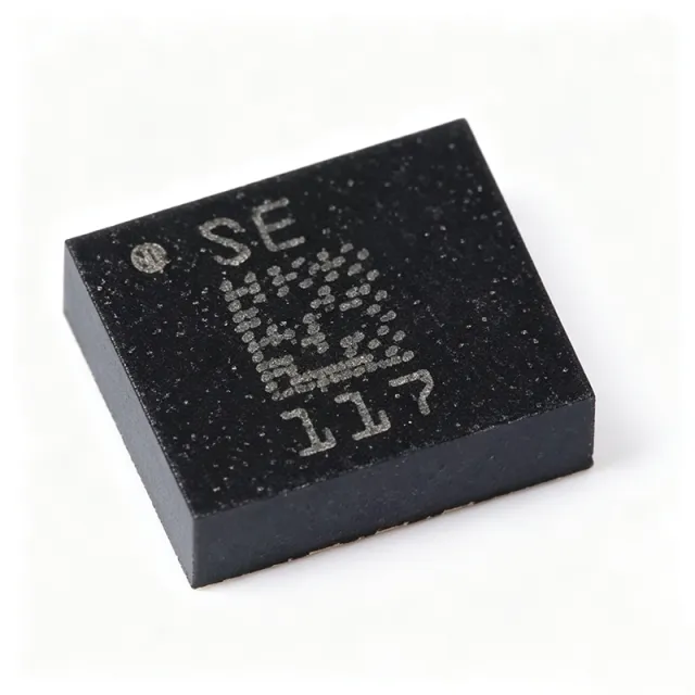
LSM6DS3TR-C - 3D Accelerometer & 3D Gyroscope | STMicroelectronics
The LSM6DS3TR-C is a high-performance 3D digital accelerometer and 3D digital gyroscope system-in-package (SiP) from STMicroelectronics, designed for consumer and industrial motion sensing applications. It features a full-scale acceleration range of ±2/±4/±8/±16 g and an angular rate range of ±125/±245/±500/±1000/±2000 dps, with a 16-bit data output for both sensors. The device operates from a 1.71V to 3.6V supply voltage and communicates via I2C or SPI interfaces, making it highly versatile for embedded systems. Data verified as of 2026-08-05. What is an inertial measurement unit (IMU)? An IMU is a sensor module that combines an accelerometer and a gyroscope to measure linear acceleration and angular velocity, respectively. The LSM6DS3TR-C is a 6-axis IMU, which is a subset of motion sensors used in a wide range of applications from smartphones to robotics. In the sensor hierarchy, an IMU falls under the category of motion sensors, which are part of the broader sensor family. This device integrates both sensors in a single package, reducing board space and simplifying design compared to discrete solutions. Key features of the LSM6DS3TR-C include an ultra-low power consumption of 0.9 mA in normal mode, a 16-bit resolution, and an embedded FIFO buffer of 8 KB that allows data batching to reduce host processor load. The device also features a programmable interrupt generator for motion detection, step detection, and tilt functions, enabling always-on applications with minimal power. The LGA-14L package (2.5 x 3.0 x 0.83 mm) is compact and suitable for space-constrained designs. Technically, the LSM6DS3TR-C uses a micro-machined silicon structure with capacitive sensing for both acceleration and angular rate. It includes a dedicated internal processing engine for advanced features like pedometer and step counter, which are hardware-accelerated to offload the host MCU. The device supports a wide operating temperature range of -40°C to +85°C, making it suitable for industrial environments. The SPI and I2C interfaces allow flexible integration with various microcontrollers. Typical applications include motion-activated user interfaces, gaming and virtual reality input devices, optical image stabilization (OIS) in cameras, and industrial vibration monitoring. The low power consumption and high resolution make it ideal for battery-powered IoT devices, where long battery life is critical. In smartphones, it enables screen rotation and step counting, while in industrial settings, it can detect machine vibration anomalies. When designing with the LSM6DS3TR-C, ensure proper decoupling of the power supply with a 100 nF capacitor close to the VDD pin, and route the I2C/SPI lines with minimal trace length to avoid signal integrity issues. The device's interrupt pins can be configured to wake the system from sleep, enabling power-efficient always-on sensing. This page synthesizes distributor pricing, drop-in alternatives, and practical design notes not found in the ST datasheet, providing a comprehensive resource for engineers evaluating the LSM6DS3TR-C for their motion sensing needs.
LSM6DSLTR - 3D Accelerometer & 3D Gyroscope iNEMO | STMicroelectronics
The LSM6DSLTR is a high-performance 3D digital accelerometer and 3D digital gyroscope system-in-package (SiP) from STMicroelectronics, designed for low-power and high-accuracy motion sensing applications. It integrates a 3-axis accelerometer and a 3-axis gyroscope in a single LGA-14L package, providing a compact solution for consumer, industrial, and IoT devices. The device features a full-scale acceleration range of ±2/±4/±8/±16 g and an angular rate range of ±125/±245/±500/±1000/±2000 dps, with a selectable output data rate (ODR) from 1.6 Hz to 6.66 kHz. The LSM6DSLTR operates from a 1.71V to 3.6V supply voltage and includes an advanced digital motion engine (DME) for always-on features such as step counting, tilt detection, and motion/tilt interrupts. An inertial measurement unit (IMU) is a device that combines accelerometers and gyroscopes to measure linear acceleration and angular velocity. The LSM6DSLTR is a 6-axis IMU, which is a subset of motion sensors used in a wide range of applications from smartphones to industrial robotics. IMUs are essential for orientation tracking, gesture recognition, and navigation systems. The LSM6DSLTR belongs to the iNEMO family of STMicroelectronics, which integrates multiple sensors and processing capabilities into a single package, enabling advanced motion sensing with minimal power consumption. Key features of the LSM6DSLTR include a low power consumption of 0.4 mA in normal mode and 0.9 mA in high-performance mode, making it ideal for battery-powered devices. It also features a 16-bit data output for both accelerometer and gyroscope, an embedded temperature sensor, and a programmable interrupt generator. The device supports I2C and SPI interfaces, allowing flexible integration with microcontrollers. The LSM6DSLTR is AEC-Q100 qualified, making it suitable for automotive applications, and is RoHS compliant. The LSM6DSLTR utilizes a micro-machined silicon structure with capacitive sensing elements, providing high stability and low noise. The device includes a 2 KB FIFO buffer that can store data to reduce host processor load, and it supports advanced features such as sensor fusion, pedometer, and significant motion detection. The device is designed to operate over a temperature range of -40°C to +85°C, ensuring reliable performance in harsh environments. Typical applications include wearable devices, smartphones, gaming controllers, industrial vibration monitoring, and automotive navigation systems. The LSM6DSLTR is particularly suited for applications requiring low power consumption and high accuracy, such as fitness trackers and smartwatches, where continuous motion tracking is essential. When designing with the LSM6DSLTR, ensure proper decoupling of the power supply with a 100 nF capacitor close to the VDD pin, and route the I2C/SPI lines with appropriate pull-up resistors. The device's interrupt pins can be configured to wake the system on motion, reducing overall power consumption in always-on applications.

LSM6DSMTR - 6-Axis IMU, ±2/±4/±8/±16 g, ±125/±245/±500/±1000/±2000 dps | STMicroelectronics
The STMicroelectronics LSM6DSMTR is a system-in-package (SiP) 6-axis inertial measurement unit (IMU) that integrates a 3D digital accelerometer and a 3D digital gyroscope, plus a temperature sensor, in a 14-pin LGA (3x2.5x0.83 mm) package. The accelerometer supports user-selectable full-scale ranges of ±2/±4/±8/±16 g and the gyroscope supports ±125/±245/±500/±1000/±2000 dps, with output data rates up to 6.6 kHz. A dedicated auxiliary SPI interface provides an independent OIS (optical image stabilization) data path for the gyroscope. An IMU (Inertial Measurement Unit) is a sensor subsystem that fuses multi-axis accelerometer and gyroscope data to deliver orientation, motion, and angular-velocity information. IMUs belong to the broader class of MEMS (micro-electromechanical systems) motion sensors and sit within inertial sensing, a foundational tier of modern sensor signal chains. The LSM6DSMTR is part of ST's iNEMO family - always-on, low-power-on, low-noise sensor modules used in smartphones, wearables, and AR/VR platforms. Key features include 0.65 mA typical current consumption in high-performance mode, integrated smart FIFO up to 4 kbyte, Android M compliance, a hardware step counter and step detector, and standard I²C/SPI primary digital interfaces. Built-in self-test, a wake-up/free-fall interrupt engine, and a tilt/6D/4D orientation function eliminate the need for host-side algorithm overhead in many use cases. The auxiliary SPI allows an image-stabilization controller to read gyro data without disturbing the main application processor. The device leverages a CMOS-process MEMS die co-packaged with an ASIC die in a single LGA, providing tight accelerometer/gyroscope cross-axis alignment and factory-calibrated offset/gain. Internal signal conditioning, ADC conversion, and digital filtering yield noise density figures suitable for high-end consumer and prosumer applications where previously only discrete FOG (fiber-optic gyroscope) class performance was acceptable. Typical applications include smartphone camera OIS/EIS, augmented-reality head tracking, wearable fitness bands, optical image stabilization modules, drone flight controllers, and gesture recognition. The auxiliary SPI + main I²C/SPI dual-bus topology lets a dedicated OIS controller access gyro data while the host application reads accelerometer data over I²C. When designing with this device, allocate one byte of INT1/INT2 routing for the step counter and another for free-fall/wake-up. Use 100 nF + 1 µF decoupling on VDD and VDDIO, place the part over a keep-out region around the LGA cavity, and respect ST's PCB pad and stencil guidelines (NSMD pads, 0.1 mm via-in-pad optional). This page synthesizes distributor pricing, drop-in alternatives, and practical design notes not found in the manufacturer datasheet.
LSM6DSO32XTR - 32g 6-Axis IMU with ML Core | ST
The STMicroelectronics LSM6DSO32XTR is an always-on 6-axis inertial measurement unit (IMU) system-in-package combining a 3-axis digital accelerometer with a full-scale range up to 32 g and a 3-axis digital gyroscope with a range up to 4000 dps, housed in a 14-pin LGA package measuring 2.5 x 3.0 x 0.83 mm. It communicates over I2C or SPI and consumes approximately 0.55 mA in high-performance mode, according to ST product data. An inertial measurement unit is a motion sensor that fuses accelerometer and gyroscope outputs to track orientation, acceleration, and rotation. Within the sensor hierarchy, the IMU sits above discrete accelerometers and gyroscopes, and forms the core motion-sensing element of smartphones, wearables, drones, industrial condition-monitoring nodes, and robotics platforms. ST's iNEMO family is a leading MEMS IMU line, and the LSM6DSO32X extends it with the widest accelerometer range in the family. Key differentiating features include the 32 g accelerometer full scale - four times the 16 g range of the standard LSM6DSO - which captures shock and vibration events without clipping. The device integrates an embedded finite state machine (FSM) and a Machine Learning Core (MLC) that run decision-tree logic on-chip, enabling always-on context detection such as fall detection, activity classification, and vibration fingerprinting with negligible host CPU load. Technically, the sensor supports output data rates up to 6.66 kHz for the accelerometer and gyroscope, a smart FIFO for offloading data, hardware low-pass and high-pass filters, and an on-chip temperature sensor. Its always-on architecture with low-power and ultra-low-power modes makes battery-powered designs practical. The X variant additionally supports Sensor Fusion Low Power (SFLP), computing a game rotation vector in hardware. Typical applications include drone and UAV flight controllers needing 32 g shock tolerance, industrial predictive-maintenance nodes detecting machine vibration signatures via the MLC, and high-impact sports wearables. ODR range and noise floor make it equally suited to premium motion tracking in AR/VR controllers. Designers should pay attention to PCB placement: mount the part away from board flex zones and vibrating masses, and follow ST's layout guidelines for the LGA pads and ground plane continuity to preserve gyro bias stability. This page synthesizes distributor pricing context, pin-compatible family alternatives, and practical design guidance beyond the raw ST datasheet, delivering information gain over generic catalog listings.