センサ
サブカテゴリ
製品 (511)

103NT-4-R025H41G - 10kΩ NTC Thermistor Glass Bead | Semitec
The Semitec 103NT-4-R025H41G is a glass-encapsulated NTC (Negative Temperature Coefficient) thermistor with a nominal resistance of 10 kΩ at 25 °C, supplied in a radial bead form factor with 25 mm insulated leads. It belongs to the Semitec NT-4 series of high-reliability glass-sealed thermistors engineered for high-temperature operation and fast thermal response, making it a preferred sensing element in medical, industrial, and scientific instrumentation. The glass encapsulation provides hermetic sealing, mechanical robustness, and chemical resistance that conventional epoxy-coated thermistors cannot match. An NTC thermistor is a type of temperature sensor whose electrical resistance falls predictably as temperature rises, following an exponential relationship characterized by its B-constant (also called B-value or B-coefficient). The B-constant of the 103NT-4-R025H41G is typically 4250 K (range), which describes how rapidly its resistance changes across the sensing range. NTC thermistors belong to the broader category of resistive temperature sensors, sitting alongside RTDs (Resistance Temperature Detectors) and thermocouples in the wider taxonomy of passive temperature transducers used in modern electronics. Key differentiating specifications of the 103NT-4-R025H41G include its 10 kΩ nominal resistance at 25 °C, a B-constant of 4250 K (typical), and a glass bead body that enables operation across a wide temperature range with rapid thermal equilibration to surrounding media. The 25 mm lead length supports through-hole mounting or custom probe assembly, while the glass envelope is resistant to moisture, solvents, and mechanical stress. From a technical-architecture perspective, the 103NT-4-R025H41G uses a sintered metal-oxide semiconductor sensing element sealed inside a hermetic glass envelope with axial Dumet-wire leads. Compared with epoxy-coated thermistors, glass encapsulation extends the operating-temperature ceiling, improves long-term drift performance, and enables use in liquid-immersion and harsh-chemical sensing. Typical applications cover medical patient monitoring probes, HVAC inlet-air sensing, 3D-printer hot-end thermal protection, laboratory water/oil bath measurement, and industrial process control loops where the glass envelope survives cleaning solvents and elevated temperatures that would degrade epoxy-coated parts. When designing with this thermistor, pair it with a precision analog front-end such as a resistor divider feeding an ADC or an op-amp-based linearization circuit, and apply the Steinhart-Hart equation for software-side temperature conversion. Use a reference resistor of 10 kΩ for a divider optimized around the sensing midpoint. This page synthesizes distributor pricing across Mouser, DigiKey, and LCSC, drop-in alternatives within the Semitec NT family, and practical design notes not consolidated in the manufacturer datasheet, providing information gain beyond stock-distributor listings.
142PC15D - 15 PSI Amplified Pressure Sensor, 3-SIP | Honeywell
The Honeywell Sensing and Productivity Solutions 142PC15D is an amplified differential pressure sensor rated for 0 PSI to 15 PSI (0 kPa to 103.42 kPa), housed in a 3-SIP through-hole module with a male 0.2 inch (5 mm) tube port. It provides a ratiometric analog voltage output proportional to applied differential pressure, powered from a single DC supply. A board mount pressure sensor is a packaged transducer that converts a pneumatic pressure differential into an electrical signal. Within the broader hierarchy, the 142PC series belongs to the pressure sensor product family, which is a subset of sensors and transducers used in industrial, medical, HVAC, and instrumentation systems. Amplified, calibrated differential sensors such as the 142PC15D integrate on-board signal conditioning, temperature compensation, and a 3-SIP package that simplifies PCB layout versus bare die transducers. Key features of the 142PC15D include a 15 PSI maximum differential pressure range, dual 1 V to 6 V analog output swing covering the full calibrated span, an 8 V supply voltage rating, and 8 mA typical supply current. The 3-SIP module provides a ported inlet that accepts a 5 mm tube, allowing pneumatic connection via flexible tubing. The amplified output eliminates the need for external op-amp signal conditioning in most applications. Technically, the device uses a piezoresistive silicon sensing cell that is ratiometric to the supply, so the output span scales with supply voltage. This simplifies ADC interfacing because the same code range is maintained regardless of supply variation. The integrated amplifier and temperature compensation circuitry provide a calibrated, linear output across the 0 PSI to 15 PSI range, reducing engineering effort versus raw sensor elements. Typical applications include HVAC duct pressure monitoring, pneumatic control systems, medical respiratory equipment, analytical instrumentation, and industrial process control. The 0 PSI to 15 PSI range is well suited to low-pressure gas flow sensing, filter pressure-drop measurement, and clean-room pressure differential verification. When designing with this part, verify that the supply voltage does not exceed the 8 V absolute maximum and provide adequate decoupling close to the supply pin. The ratiometric output simplifies ADC interfacing but requires that the ADC reference voltage be derived from the same supply used to power the sensor for maximum accuracy. This page synthesizes distributor pricing across nine sources, cross-reference availability, drop-in alternative candidates, and practical design notes that supplement the manufacturer datasheet with sourcing and integration context.
9012ADW7S1M12 - 38-340bar Differential Pressure Switch | Telemecanique
The Telemecanique Sensors 9012ADW7S1M12 is an industrial electro-mechanical pressure switch with a sealed piston sensor, designed for hydraulic and fluid-power applications in the 38 to 340 bar (550 to 4930 psi) differential pressure range. Housed in a die-cast zinc-alloy enclosure with PG13.5 cable gland and G3/8 process connection, it provides SPDT switch output rated for 3 A at 120-240 V DC and 5 A at 120-600 V AC, making it suitable for direct control of contactors, solenoid valves, and alarm circuits in heavy-industrial machinery. An industrial pressure switch is an electro-mechanical device that converts a fluid pressure signal into a discrete electrical switch action at a preset actuation threshold. Within the broader sensor hierarchy, pressure switches sit between simple pressure transducers (analog output) and full PLC-integrated pressure transmitters (4-20 mA / IO-Link) — they provide local setpoint-based control without requiring a controller, which is why they remain widely deployed on pumps, compressors, hydraulic power packs, and HVAC chiller plants. The 9012 series from Telemecanique (Schneider Electric) belongs to the legacy ACW/ADW family of compact, field-adjustable piston-style differential switches. Key specifications of the 9012ADW7S1M12 include a working pressure range of 38 to 340 bar (550 to 4930 psi), a differential (adjustable) setpoint with sealed piston actuation, media compatibility with hydraulic fluid and lubricating oil, an operating temperature window of -25 °C to +120 °C, and IP65 ingress protection suitable for wash-down industrial environments. The supply-voltage range of 120-240 V DC and 120-600 V AC reflects the legacy ACW/ADW family’s design intent for direct connection to industrial control gear without intermediate relays. Technically, the 9012ADW7S1M12 uses a sealed piston sensing element coupled to a snap-action SPDT microswitch. The piston seal isolates the process fluid from the switch mechanism, improving media compatibility versus diaphragm-only designs at high pressures. Adjustment is performed via an external setpoint screw, and the differential (dead-band) is fixed by the piston-spring geometry rather than user-configurable. The zinc-alloy housing provides mechanical robustness and EMI shielding, while the PG13.5 cable gland allows field termination of power and signal conductors. Typical applications include hydraulic power-pack high-pressure cut-out, compressor discharge over-pressure protection, lubrication-system pressure verification, and machine-tool coolant-pressure monitoring. The wide AC/DC voltage rating allows the same part to control both 230 V AC contactors and 24-240 V DC solenoid valves without hardware variants. When designing with this part, note that RS Components has flagged it as a discontinued line item. Engineers specifying new designs should evaluate the Schneider Electric 9012 series replacement equivalents or consider migrating to XMLR / OsiSense XMLG pressure transmitters for new platforms. Existing maintenance stock and refurbishment workflows continue to use the 9012ADW7S1M12 as a direct-fit spare. This page synthesizes distributor pricing, electrical ratings, application guidance, and Schneider 9012 family context that are not consolidated in any single manufacturer document, providing an engineer-ready summary in one place.

A1102LLHLT - Unipolar Hall Effect Switch, 180G Trip, SOT-23W
The Allegro MicroSystems A1102LLHLT is a continuous-time unipolar Hall-effect digital switch with open-drain output, delivered in a 3-pin SOT-23W surface-mount package. It operates across a 3.8 V to 24 V supply range, switches at a 180 Gauss (typ.) magnetic trip point with a 125 Gauss release point, and is qualified to the extended -40 °C to +150 °C automotive temperature range. A Hall-effect switch is a magnetic sensor whose output changes state when the applied magnetic flux density crosses a programmed threshold. Compared with reed switches, Hall ICs offer solid-state reliability, sub-microsecond response, and integration of the sensing element, signal conditioning, and output driver in a single silicon die. The A1102 belongs to Allegro's continuous-time family: the on-chip oscillator drives a dynamic-cancellation chopper-stabilized Hall plate, eliminating the residual offset of DC-biased Hall elements and yielding a stable switch point over temperature and supply. Key features include a south-pole-only unipolar transfer function (output turns on when |B| exceeds Bop and off when |B| falls below Brp), 20 kHz typical chopping frequency for clean output, low quiescent current, 30 V absolute-maximum supply tolerance, and reverse-battery protection on the supply pin. The open-drain output requires an external pull-up resistor, simplifying interface to 3.3 V, 5 V, or 12 V logic rails without level shifting. Architecturally, the device combines a BiCMOS Hall sensing front-end, a precision comparator with trimmed thresholds, an open-drain DMOS output stage, and on-chip protection (reverse-supply, over-voltage, and output ESD). The BiCMOS process enables fast power-on (<10 µs) and low-noise operation without the offset drift seen in older bipolar Hall ICs, while the chopper-stabilized front end virtually eliminates the residual offset that would otherwise shift the switch point with mechanical stress. Typical applications include automotive seat-belt buckle detection, gear-shift and transmission position sensing, BLDC motor commutation triggers, valve and solenoid position feedback, consumer appliance lid/door interlocks, and contactless limit switches. The wide 3.8 V-24 V supply range allows direct connection to 12 V automotive rails without an upstream regulator. Designers should provide a bypass capacitor of at least 0.1 µF close to the supply pin and a pull-up resistor (typically 10 kΩ) on the output. Place the device so the brand-side marking aligns with the target magnet's pole direction; the sensitive axis is perpendicular to the package top. This page synthesizes distributor pricing, drop-in SOT-23W alternatives, and practical design notes that the manufacturer datasheet alone does not aggregate.

A1391SEHLT-T - Micropower Linear Hall Effect Sensor | Allegro
The Allegro MicroSystems A1391SEHLT-T is a micropower 3 V linear Hall-effect sensor IC with tri-state output and user-selectable sleep mode, housed in a 6-lead MLP/DFN (2 x 3 mm) surface-mount package. It provides an analog output voltage that is directly proportional to an applied magnetic field, with a typical sensitivity of 2.5 mV/G and a 1.4 mm thin-profile package. A linear Hall effect sensor is a type of magnetic position sensor that converts the flux density of an applied magnetic field into a proportional analog voltage. Hall-effect sensors belong to the broader category of magnetic sensors, which sit within the transducer family alongside temperature, pressure, and current sensors. The Act as contactless replacements for mechanical potentiometers and reed switches, delivering higher reliability, finer resolution, and immunity to mechanical wear. Key features of the A1391SEHLT-T include 3.1 V minimum supply voltage, micropower consumption for battery-operated designs, integrated temperature compensation circuitry that reduces the intrinsic sensitivity drift of the Hall element, and a low-noise small-signal high-gain amplifier on the same BiCMOS die. The device also offers a tri-state (high-impedance) output for wire-ORed multiplexed ADC sampling, plus an enable/sleep pin for power gating in duty-cycled systems. The BiCMOS monolithic architecture integrates the Hall element, chopper-stabilized amplifier, and temperature-compensation network on a single die, achieving low offset, low noise, and a stable quiescent output voltage (VREF) at zero field. The user-selectable sleep mode enables system designers to drop quiescent current during idle windows, an absolute measure in efficiency-critical designs. Typical applications include cellular phones, digital still cameras, portable tools, white-goods position feedback, and battery-operated consumer electronics where contactless rotary or linear position sensing is required. The wide supply range down to 3 V and microamp-level sleep current suit coin-cell and lithium-polymer powered products. When designing with this device, place a 1 nF to 100 nF bypass capacitor close to the supply pin and keep the high-current switching traces away from the Hall element to avoid magnetic and electrical crosstalk. Verify the magnetic circuit produces the rated field range at the IC location; the A1391SEHLT-T is sensitive to stray fields from nearby motors or inductors. This page synthesizes Allegro datasheet specifications, distributor stock and pricing, same-family drop-in alternatives (A1392/A1393/A1395 in identical DFN-6), and practical design notes not found in the manufacturer datasheet.

ACS37800KMACTR-015B5-SPI - Isolated ±15A Power Monitor IC, SPI, 16-SOIC | Allegro
The Allegro MicroSystems ACS37800KMACTR-015B5-SPI is a galvanically isolated, programmable AC and DC power monitoring IC with integrated current and voltage sensing channels, housed in a 16-pin SOIC package. It features bidirectional current sensing up to ±15.5 A (15B5 variant), reinforced isolation, and an SPI digital interface for host MCU communication. The part combines a precision Hall-effect current sensor with a resistive divider voltage sense path, producing instantaneous, RMS, and accumulated energy parameters in on-chip registers. An isolated power monitor IC is a single-chip device that measures load current and supply voltage on a high-voltage bus while maintaining galvanic isolation between the sensed node and the low-voltage digital controller. Within the broader taxonomy, this places the ACS37800 in the current sensor -> sensor IC -> power management IC -> semiconductor hierarchy. Compared to shunt-resistor + isolated-amplifier designs, an integrated monitor IC reduces PCB area, eliminates shunt resistor power dissipation losses, and removes external ADC loading on the host MCU by performing metrology internally. Key features include ±15.5 A bidirectional current range, integrated zero-crossing detection for AC line synchronization, programmable overcurrent and overvoltage flagging with hardware pins, on-chip temperature compensation, and CRC-protected SPI transactions at up to 10 MHz. The 16-SOIC (MA) package carries 1418 V reinforced isolation per UL/TUV standards, removing the need for optocouplers or isolated ADC front-ends. The 015B5 ordering code denotes ±15.5 A range, 5 V supply, and SPI digital output variant. The ACS37800 uses Allegro's proven Hall-effect front end combined with a 16-bit sigma-delta conversion chain and an embedded DSP that computes VRMS, IRMS, instantaneous power, line frequency, and active/active-fundamental energy on-chip. Designers access computed quantities directly rather than raw ADC counts, offloading the host MCU. The device supports 50 Hz to 60 Hz nominal mains plus DC bus measurement, making it suitable for single-phase AC and high-voltage DC power systems alike. Typical applications include solar inverter string monitoring, EV charging station energy metering, industrial PLC power diagnostics, and 48 V telecom/AI-server current monitoring. The wide operating temperature range of -40C to +125C and reinforced isolation also make it well-suited for harsh industrial and automotive 12 V/48 V environments. When designing with this device, route the high-voltage bus through the integrated Hall loop on pins 1-4 to ensure proper current sensing geometry and minimize external magnetic field interference. Provide a low-ESR 1uF decoupling capacitor on the secondary-side VDD pin and keep SPI traces short and impedance-controlled. This page synthesizes distributor pricing, drop-in same-package alternatives, application examples, and design notes not found in the manufacturer datasheet alone, helping engineers select, source, and design with the ACS37800KMACTR-015B5-SPI faster than datasheet-only references.
ACS37800KMACTR-030B3-I2C - Isolated ±30A AC/DC Power Monitor | Allegro
The Allegro MicroSystems ACS37800KMACTR-030B3-I2C is an isolated, programmable AC and DC power monitoring IC integrating voltage, current, and power measurement with reinforced galvanic isolation in a 16-pin SOIC (MA) package. The device supports bidirectional current sensing from -30 A to +30 A, operates from a single 3.3 V supply, and exposes a digital I2C interface for configuration and readback. Its 480 VRMS nominal voltage range with ±980 V peak capability makes it suited to single-phase AC mains and high-voltage DC bus monitoring. A power monitoring IC combines current sensing, voltage sensing, and computational resources to compute real power, apparent power, reactive power, RMS values, and energy on-chip, freeing the system MCU from these tasks. The ACS37800 family belongs to the broader category of integrated Hall-effect current sensor ICs and is positioned above discrete shunt-resistor amplifiers because it provides inherent galvanic isolation without an external isolation barrier, reducing PCB area, BOM count, and firmware complexity. Key features of the -030B3-I2C variant include ±30 A bidirectional current range, factory-trimmed gain and phase calibration, integrated voltage divider with programmable ratio, zero-crossing detection for AC line synchronization, user-programmable thresholds and response times, and built-in temperature compensation. The reinforced isolation supports 5 kVRMS withstand voltage, and the digital interface delivers 16-bit voltage and current readings with integrated energy accumulators. The architecture pairs a Hall-effect sensor element with a sigma-delta ADC and a dedicated DSP-style calculation engine. Each conversion cycle updates VRMS, IRMS, active power, reactive power, apparent power, power factor, and frequency. The integrated voltage channel allows single-package implementation of single-phase power metering without external PTs or high-voltage op-amps. Typical applications include AC/DC power supplies, server and telecom PSU load monitoring, smart circuit breakers, sub-metering and e-Metering, solar inverters, EV charging stations, industrial motor drives, and battery management systems. The I2C variant specifically targets designs where a host MCU samples telemetry on demand rather than the SPI variant's continuous high-speed data stream. Designers should follow Allegro's PCB layout guidelines for the MA package: keep high-voltage traces outside the reinforced-isolation creepage region and provide adequate copper pours for thermal dissipation at high DC currents. Compared with discrete shunt + op-amp + isolator solutions, this IC reduces CPU cycles and PCB area by integrating isolation, sensing, and calculation.
ACS37800KMACTR-090B3-I2C - Isolated AC/DC Power IC | Allegro
The Allegro MicroSystems ACS37800KMACTR-090B3-I2C is a galvanically isolated, programmable AC and DC power monitoring IC that simultaneously measures voltage, current, and power from a single 3.3 V supply, delivering digital outputs via an I²C bus. It combines Allegro's Hall-effect current sensing technology with a dedicated metrology engine, supports a current sensing range up to ±90 A, and features reinforced isolation for high-voltage single-phase applications. The device ships in a 16-pin SOIC (KMAC) package with 1000-piece tape-and-reel packaging. A power monitoring IC is a semiconductor device that combines analog front-end current sensing (typically Hall-effect or shunt-based), voltage sensing, and computation logic to deliver real-time power, energy, and quality metrics to a host MCU. The ACS37800 sits within the broader hierarchy of power management semiconductors, alongside voltage regulators, supervisors, and motor drivers, and serves as a digital alternative to discrete op-amp + shunt resistor + ADC solutions. Reinforced isolation means the high-voltage conductor and the low-voltage digital domain are separated by a certified insulation barrier, eliminating the need for external isolators. Key differentiating features include a 1 kHz measurement bandwidth, factory-trimmed accuracy, user-programmable overcurrent fault response of 5 µs (typical), user-programmable undervoltage and overvoltage RMS thresholds, dedicated voltage or current zero-crossing pin, and flexible 1 kHz bandwidth operation. The integrated metrology engine offloads the host processor by computing RMS, active power, apparent power, reactive power, and power factor internally, reducing CPU cycle consumption and PCB area. Technically, the part uses a differential Hall-effect front end that rejects common-mode external magnetic fields, paired with a high-resolution sigma-delta ADC and digital signal processing block. The reinforced galvanic isolation is implemented on-chip via Allegro's proprietary micro-transformer isolation barrier, achieving UL-recognized isolation ratings suitable for line-voltage applications. Typical applications include solar inverter DC-side monitoring, single-phase AC load metering, industrial motor drive input power measurement, EV charging station energy metering, smart circuit breakers, and home appliances requiring accurate AC and DC energy reporting. The wide ±90 A sensing range supports both sub-kW consumer loads and multi-kW industrial systems. When laying out, route the I2C SDA/SCL traces with 4.7 kΩ pull-ups to VCC, keep the high-voltage current-carrying conductor centered over the integrated conductor loop, and provide adequate clearance beneath and around the KMAC package to preserve the reinforced isolation rating. This page synthesizes distributor pricing, drop-in alternatives, and design notes not consolidated in the manufacturer datasheet.

ACS70331EOLCTR-005U3 - 5A GMR Unidirectional Current Sensor | Allegro
The Allegro MicroSystems ACS70331EOLCTR-005U3 is a high-sensitivity, 1 MHz bandwidth, giant-magnetoresistive (GMR) based current sensor IC supplied in an 8-pin SOIC package (0.154", 3.90 mm body width). It is factory-trimmed for 5 A unidirectional primary current measurement and operates from a single 3.3 V supply. Per the Allegro product family description, the device is targeted at sub-5 A current sensing applications and is Allegro's first integrated, high-sensitivity current sensor IC in this range. GMR technology is approximately 25 times more sensitive than conventional Hall-effect sensors, enabling a low-noise analog output and sub-microsecond response time. The Allegro datasheet family lists a typical response time of 535 ns. The part is offered in four factory-programmed sensitivity/offset variants (U3/U5/B3/B5 suffixes) to optimize performance over different current ranges. Note: Mouser lists the lifecycle status as NRND (Not Recommended for New Designs). A current sensor IC is a transducer that converts the magnetic field produced by a primary current into a proportional analog voltage or current output, allowing a microcontroller or ADC to monitor system power consumption without inserting a shunt resistor in the load path. The ACS70331 belongs to the integrated current sensor category (current sensor IC > magnetic current sensor > GMR current sensor > power monitoring IC > analog sensor IC > semiconductor). Compared with traditional Hall-effect ICs, GMR-based sensors offer much higher sensitivity (mV/A), lower noise, and faster response, which is particularly important for detecting fast load transients in motor drives, battery management, and point-of-load monitoring. Key features include: a 5 A primary current range optimized for low-current applications; GMR-based sensing providing approximately 25x the sensitivity of Hall-effect sensors; a typical response time of 535 ns; a low-noise analog ratiometric output proportional to primary current; and factory-trimmed sensitivity/offset to reduce external calibration. The 8-pin SOIC surface-mount package has a low thermal profile and supports automated assembly. The device's footprint and pinout are footprint-compatible with the bidirectional (B-suffix) variants in the same family. Typical applications include battery monitoring in handheld and IoT devices, USB-C current monitoring, point-of-load monitoring on 3.3 V rails, small motor and fan current monitoring, and low-side/high-side current sensing in compact power-conversion stages. The unidirectional (U3) variant is intended for monitoring current flowing in one direction only, whereas the bidirectional (B3/B5) variants are suited for charge/discharge monitoring such as USB-PD current advertisement. When designing with this part, ensure the primary current path is routed through the integrated SOIC-8 lead frame (per Allegro's recommended PCB layout). Decouple VCC with a local 0.1 microfarad ceramic capacitor placed close to the supply pin. Account for ratiometric output scaling when using an ADC reference tied to the same 3.3 V rail. This page synthesizes distributor pricing, drop-in pin-compatible alternatives in the same SOIC-8 footprint, and practical PCB layout notes not all consolidated in a single manufacturer resource.
ACS712 - Hall-Effect Linear Current Sensor IC | Allegro MicroSystems
The Allegro MicroSystems ACS712 is a fully integrated, Hall-effect-based linear current sensor IC housed in an 8-pin SOIC (LC) package that delivers economical and precise solutions for AC or DC current sensing in industrial, commercial, and communications systems. The ACS712 family is offered in three factory-trimmed primary-current ranges: ±5 A (ACS712-05B), ±20 A (ACS712-20B), and ±30 A (ACS712-30B), with sensitivity scaling inversely with range at 185 mV/A, 100 mV/A, and 66 mV/A respectively. A Hall-effect current sensor is a non-contact transducer that exploits the Lorentz force principle: current flowing through an internal low-resistance copper conduction path generates a magnetic field proportional to the amperage, which an on-chip Hall element converts into a ratiometric analog output voltage. This places Hall-effect current sensors at the same level in the sensing hierarchy as shunt-resistor amplifiers (e.g., INA219) and current transformers (CTs); Hall sensors are uniquely galvanically isolated, compact, and bidirectional by construction, while shunt amplifiers offer higher bandwidth and CTs require AC excitation. Key features include a galvanically isolated current path (no shunt resistor required), sub-ohm internal conductor resistance (1.2 mΩ typical) for minimal insertion loss, a 5.0 µs output rise time in response to step input, and a 50 kHz small-signal bandwidth. The device operates from a single 5 V supply, draws a low quiescent current, and provides a stable zero-current output of VCC/2 (≈2.5 V at 5 V supply) for bidirectional measurement around the mid-rail. Proprietary integrated digital temperature compensation trims sensitivity and offset across the −40°C to +85°C operating range. The architecture uses a precise, low-offset linear Hall circuit placed near the copper conduction path; close proximity between magnetic signal and transducer maximizes device accuracy. Differential sensing cancels external stray fields, and a low-impedance output stage buffers the ratiometric output for direct connection to an ADC input or comparator threshold. Typical applications include motor control and load detection in robotics and white goods, switched-mode power supply feedback for overcurrent protection, battery management in e-bikes and UPS systems, and 3D printer / CNC spindle current monitoring. The SOIC-8 footprint suits both hand-soldered breakouts and high-density SMT production. When designing, place a low-ESR bypass capacitor close to VCC and route the primary current conductor through the on-package copper trace to maintain specified accuracy; verify the output zero point at no current before each conversion to remove thermal drift.
ACS756SCA-050B-PFF-T - 50A Bidirectional Hall-Effect Current Sensor | Allegro
The Allegro MicroSystems ACS756SCA-050B-PFF-T is a fully integrated, Hall-effect-based linear current sensor IC with 3 kVRMS voltage isolation and a low-resistance current conductor, rated for ±50 A primary current sensing in a 5-pin CA (PFF lead form) through-hole package. It features 40 mV/A sensitivity, 120 kHz bandwidth, ratiometric analog output, and a typical response time of 3 µs, supplied from a single 5 V rail with 14 mA maximum quiescent current. What is a Hall-effect current sensor? A Hall-effect current sensor is a contactless transducer that uses the Lorentz force on charge carriers in a magnetic field to produce a voltage proportional to the current flowing through an integrated primary conductor. Within the broader IC taxonomy, it belongs to the magnetic-sensor family, sits under the current-sensor sub-family, and ultimately falls within the analog signal-chain / power-management hierarchy. Compared to shunt-resistor + op-amp solutions, integrated Hall-effect sensors provide galvanic isolation (3 kVRMS here), low insertion loss, and a compact single-IC footprint. Key features include bidirectional current measurement across the full ±50 A range, 1.5 mΩ primary conductor resistance to minimize power loss, factory-trimmed sensitivity and offset for high accuracy, and a monolithic design that eliminates the need for external sense resistors or isolation barriers. The device is internally protected by a 3 kVRMS isolation barrier between the high-current primary loop and the low-voltage analog signal side, allowing direct MCU/ADC interface. Architecturally, the ACS756SCA-050B-PFF-T integrates the primary current-carrying loop, Hall-effect transducer element, chopper-stabilized signal chain, and output amplifier on a single die. The chopper-stabilization technique cancels the Hall-element's temperature drift and stress-induced offset, yielding a stable ratiometric output centered at VCC/2 = 2.5 V with ±0.65 V full-scale swing at ±50 A (40 mV/A). The PFF lead form provides through-hole strain relief and PCB creepage clearance to support the rated isolation voltage. Typical applications include motor-control current monitoring in industrial drives, battery-management systems (BMS) for current-in/out measurement, solar inverter input/output sensing, and overload protection in switched-mode power supplies. The bidirectional range is particularly useful for applications where current reverses during normal operation, such as regenerative braking in e-bikes and motor drives. When designing with this part, place the device so the high-current conductor traces enter and exit the IP+ and IP- pins with adequate copper cross-section. Decouple VCC with a 0.1 µF ceramic capacitor placed within 5 mm of the lead, and add a 1 µF bulk capacitor for noise suppression on the output pin. This page synthesizes distributor pricing, drop-in same-brand alternatives (other ACS756 temperature grades), and practical design notes not found in the manufacturer datasheet.

AD595AQ - Type K Thermocouple Amplifier w/ CJC, 14-CERDIP | Analog Devices
The Analog Devices AD595AQ is a monolithic Type K thermocouple amplifier with on-chip cold-junction compensation (CJC), factory-trimmed to produce a high-level 10 mV/°C output directly from a thermocouple signal, packaged in a 14-pin CERDIP (Q) hermetic package. The part combines an ice-point reference, a precision pre-calibrated instrumentation amplifier, and a thermocouple-linearization network on a single bipolar die, eliminating the discrete cold-junction circuit, op-amp, and reference that traditional Type K designs require. According to the Analog Devices AD594/AD595 datasheet, the device operates from a single +5 V supply and supports a calibrated measurement range of 0 °C to +300 °C (Q grade). A thermocouple amplifier is a specialized analog front-end IC that conditions the microvolt-level output of a thermocouple - two dissimilar metals joined at a hot junction whose Seebeck voltage tracks temperature - and translates it into a standardized, low-impedance signal that an ADC, controller, or display can read directly. Within the signal-chain hierarchy, the AD595AQ sits between the sensor layer (the Type K probe) and the data-acquisition layer (the ADC or MCU), performing the cold-junction compensation, linearization, and amplification functions that would otherwise demand five to ten discrete components. Key features include factory-trimmed NIST Type K linearization, 10 mV/°C nominal scaling (versus the raw Type K Seebeck coefficient of roughly 41 µV/°C, an internal gain of ~244×), ±1 °C (A grade) or ±2.5 °C maximum calibration error over the rated span, pin-strappable setpoint-controller mode for switched-output thermostat operation, and an ice-point-trimmed reference accurate to ±0.05 °C/°C of board temperature drift. Internal amplifier bandwidth supports both continuous linearization and PWM-style setpoint use. Typical applications include industrial oven/ furnace profiling, HVAC duct and stack-gas monitoring, laboratory benchtop temperature instruments, and standalone Celsius transducers driving panel meters or PLC analog inputs. The hermetic 14-CERDIP package suits legacy military/aerospace systems, downhole oil/gas tools, and other environments where plastic SOIC moisture absorption is unacceptable. Note that ADI now classifies the AD595 as "NOT RECOMMENDED FOR NEW DESIGNS," so the AD595AQ is best suited to existing designs, repair stock, or replacement of obsolete industrial boards. When designing with the AD595AQ, bypass +VS to ground with 0.1 µF ceramic as close to the IC as possible, connect the thermocouple inputs with twisted-pair or shielded wire routed away from switching noise, and remember that the on-chip compensation only addresses the board-side cold junction - any heat conducted down the probe wires will still introduce error. The Q grade is calibrated for 0-300 °C; for higher ranges the C grade (0-1000 °C) is a drop-in alternative. This page synthesizes distributor pricing, drop-in ADI same-package alternatives, and practical design notes beyond what the manufacturer datasheet alone provides, helping engineers source, substitute, and integrate the AD595AQ with confidence.
AD694ARZ - 4-20mA Current Loop Transmitter 16-SOIC | Analog Devices
The Analog Devices AD694ARZ is a monolithic current transmitter that accepts high-level voltage inputs and drives a standard 4-20 mA (or 0-20 mA) current loop, housed in a 16-pin SOIC_W package with an exposed thermal pad. It integrates three on-chip amplifiers, a precision 10.000 V reference, and a programmable input scaling stage that delivers precalibrated 0 V to 10 V or 0 V to 2 V input ranges with no external trims. The device operates from a single 4.5 V to 36 V supply (or dual ±15 V supplies), supplies the loop from the same rail, and draws a typical 23 mA quiescent current at full-scale 20 mA output. A current transmitter IC is a category of sensor and process-control interface that converts a low-level voltage command signal into a noise-immune 4-20 mA current for transmission over long industrial cables. The 4-20 mA standard is preferred in process control because current is unaffected by ground-loop voltage drops and the 4 mA "live-zero" lets a single broken wire be detected as a fault. The AD694 sits in the broader hierarchy of sensor/detector interface ICs (which also include RTD/thermocouple conditioners and LVDT drivers) under the power management and signal-chain function blocks. Key feature highlights include a laser-trimmed input offset of 150 µV and 90 dB CMRR for rejection of common-mode noise from field wiring, a -3 dB bandwidth of 300 kHz to support multiplexed settling, and selection between 4-20 mA or 0-20 mA output ranges via a single logic pin. A wide 4.5 V to 36 V power supply range accommodates both factory-floor 24 V busses and legacy ±15 V instrumentation racks, while the on-board 10 V reference can be used to excite external bridges or potentiometers. Architecturally, the AD694 combines a precision input op-amp, a V-to-I conversion loop with sense resistor, and the buffered 10 V reference in a single bipolar/CMOS process die. The exposed pad of the SOIC_W package provides a low thermal resistance path for dissipating loop-compliance losses at high supply voltages. Typical applications include industrial process-control transmitter heads for pressure, temperature, and flow sensors; PLC analog output modules driving valves and actuators; factory-automation analog I/O; and SCADA remote terminal units. The 4-20 mA output integrates natively with HART modems for bidirectional digital communication over the same pair of wires. When using the AD694ARZ, choose the 0 V to 10 V or 0 V to 2 V precalibrated input by strapping the input-range pin, and verify that the supply rail exceeds the loop-compliance voltage headroom plus the 10 V reference plus 2 V. Use the exposed pad for thermal relief at compliance voltages above 30 V. This page synthesizes distributor pricing, drop-in alternatives (AD694BRZ, AD694AQ) and practical design notes not found in the standalone manufacturer datasheet.
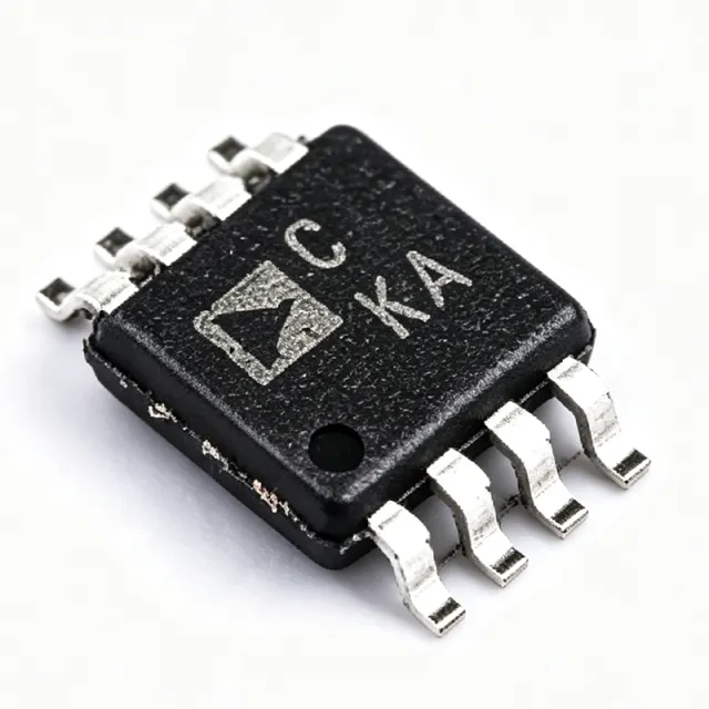
AD7314ARMZ - 10-Bit Digital Temp Sensor SPI | Analog Devices
The AD7314ARMZ from Analog Devices is a complete temperature monitoring system in an 8-lead MSOP (uSOIC) package. It integrates a bandgap temperature sensor and a 10-bit successive-approximation ADC to digitize temperature with 0.25 degree C resolution, an accuracy of +/-2 degree C, and an operating range of -35 degree C to +85 degree C. A digital temperature sensor is an integrated circuit that converts ambient temperature into a digital output using an internal sensing element and an analog-to-digital converter. These devices sit within the broader temperature sensor family alongside analog-output and thermistor solutions, and they form the sensing layer of thermal management, system protection, and performance-optimization subsystems in industrial, networking, and consumer electronics. Key features include a wide 2.65V to 5.5V supply range, an SPI/QSPI/MICRO-WIRE compatible serial interface for direct microcontroller connection, a shutdown mode for battery-powered designs, and an ID pin with internal 1k ohm pull-down that lets a host distinguish multiple devices on a shared bus. The 10-bit output yields 0.25 degree C steps, sufficient for fan control and over-temperature throttling loops. Architecturally, the bandgap sensor produces a voltage proportional to die temperature, which the on-chip SAR ADC converts on demand under host control. Read and write operations over the flexible serial interface allow configuration and data retrieval, while shutdown cuts quiescent current between conversions, conserving energy in portable and embedded systems. Typical applications include thermal management in servers and networking equipment, temperature monitoring in industrial controllers, and environmental sensing in consumer and portable electronics. Low voltage operation and the compact MSOP footprint suit space-constrained PCBs. Design tip: decouple VDD with a 0.1uF ceramic capacitor close to the pin and keep thermal paths short for accurate die-to-ambient tracking. Use the ID pin carefully to avoid bus contention in multi-device systems.
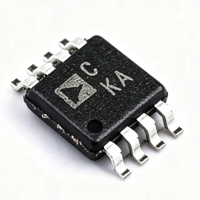
AD7314ARMZ-REEL7 - 10-Bit Digital Temp Sensor | Analog Devices
The AD7314ARMZ-REEL7 from Analog Devices is a complete temperature monitoring system in an 8-pin uSOIC (MSOP) package. It integrates a bandgap temperature sensor and a 10-bit ADC to digitize temperature readings with a resolution of 0.25C. The device operates over a temperature range of -35C to +85C and supports a supply voltage from 2.65V to 5.5V. Its flexible serial interface allows easy connection to most microcontrollers, making it ideal for space-constrained applications. A digital temperature sensor is an integrated circuit that converts ambient temperature into a digital output, typically using an internal bandgap reference and an analog-to-digital converter. In the hierarchy of temperature sensing, the AD7314 is a local digital temperature sensor, part of the broader temperature sensor family. Unlike analog sensors that output a voltage or current proportional to temperature, digital sensors provide a direct digital reading, simplifying interface design and improving noise immunity. Key features include 10-bit resolution with 0.25C LSB, a wide supply range of 2.65V to 5.5V, and low power consumption suitable for battery-powered devices. The serial interface is SPI/QSPI/MICROWIRE compatible, and the device includes a shutdown mode for power saving. The 8-lead MSOP package measures approximately 3mm x 3mm, ideal for portable and space-limited designs. Technically, the AD7314 uses a bandgap temperature sensor producing a voltage proportional to absolute temperature, digitized by a successive-approximation ADC. The device guarantees accuracy of plus or minus 2C over the full temperature range per the ADI datasheet. A power-on reset ensures valid output immediately after power-up. Typical applications include temperature monitoring in portable electronics, battery management systems, industrial process control, environmental sensing, and medical devices. Its small footprint and low power suit wearable devices and IoT nodes. When designing with the AD7314, ensure the supply voltage stays within the specified range and the SPI lines are properly terminated. No external calibration is required, but use adequate supply decoupling (0.1uF ceramic close to the VDD pin) for optimal performance.
ADIS16547 - Tactical Grade 6-DOF IMU | Analog Devices
The ADIS16547 is a complete inertial system from Analog Devices that integrates a triaxis gyroscope and a triaxis accelerometer into a single module. It is designed for tactical-grade applications requiring high accuracy and stability. The device is factory calibrated for sensitivity, bias, and alignment, ensuring consistent performance across units. The ADIS16547 is housed in an aluminum package measuring approximately 47 mm × 44 mm × 14 mm and includes a standard connector interface for easy integration. An inertial measurement unit (IMU) is a device that measures angular rate and linear acceleration using gyroscopes and accelerometers. IMUs are essential components in navigation, stabilization, and motion control systems. The ADIS16547 provides six degrees of freedom (6-DOF) sensing, combining three axes of gyroscopic data with three axes of acceleration data. This enables precise tracking of an object's orientation and movement in three-dimensional space. Key features of the ADIS16547 include its tactical-grade performance, which offers low noise and high bias stability. The device operates over a wide temperature range and provides a digital SPI interface for communication with microcontrollers or processors. The factory calibration eliminates the need for user-level calibration, reducing development time and complexity. The aluminum package provides robust mechanical protection and thermal management. The ADIS16547 uses a signal chain that processes data at a rate of fSM when using the internal sample clock. This architecture optimizes dynamic performance and ensures accurate measurement of fast-changing motion. The device supports multiple sample rates and filter options, allowing designers to tailor the output to their specific application requirements. The SPI interface enables high-speed data transfer and configuration of the device's registers. Typical applications for the ADIS16547 include industrial automation, robotics, unmanned aerial vehicles (UAVs), platform stabilization, and navigation systems. Its tactical-grade performance makes it suitable for applications where precision and reliability are critical. The device's compact form factor and standard connector simplify integration into existing designs. When designing with the ADIS16547, it is important to consider the power supply requirements and ensure proper decoupling. The device should be mounted securely to minimize mechanical stress, which can affect sensor accuracy. Additionally, the SPI interface should be configured correctly to achieve the desired data rate and filtering.
ADTF3175 - 1MP iToF 3D Depth Module | Analog Devices
The Analog Devices ADTF3175 is a complete 1 megapixel Time-of-Flight (ToF) module for high-resolution 3D depth sensing and machine vision systems, integrating the ADSD3100 CMOS indirect-ToF (iToF) imager together with a lens, optical band-pass filter, infrared illumination source, and onboard power regulation in a single 75 mm x 75 mm open-frame package. It delivers 1024 H x 1024 V depth resolution with a 3.5 µm x 3.5 µm pixel pitch and outputs image data over a 4-lane MIPI CSI-2 Tx interface to the host processor. According to the Analog Devices datasheet, the module is factory calibrated across multiple operating modes, enabling out-of-box depth maps without per-unit calibration. A Time-of-Flight module is an optoelectronic subsystem that measures distance by emitting modulated infrared light and measuring the phase shift of the light reflected from a target. In an indirect ToF (iToF) architecture, every pixel simultaneously collects four phase-shifted samples in a single exposure, which are then mathematically combined to compute depth. The ADTF3175 sits in the system hierarchy as a depth-sensing subassembly above the image sensor (ADSD3100) and below the perception layer (typically paired with the ADSD3500 depth ISP). Key features include a 1 megapixel CMOS iToF imager with 3.5 µm pixels, an integrated 940 nm IR illuminator with eye-safety class-1 consideration, and a calibrated depth range from approximately 0.2 m to several meters depending on mode. The 4-lane MIPI CSI-2 output is electrically compatible with common application processors and the bundled EVAL-ADTF3175D-NXZ kit pairs the module with the ADSD3500 depth ISP for full depth-map generation. Fully calibrated multi-mode operation reduces OEM integration time versus discrete iToF assemblies. Typical applications include AR/VR depth capture, gesture recognition, robotics navigation, machine vision bin picking, people counting, and biometric 3D face authentication. The 75 x 75 mm open-frame form factor is intended for embedded integration rather than sealed consumer products. Compared to discrete iToF designs that require custom optics and per-unit calibration, the ADTF3175 delivers a factory-calibrated module that compresses optical, illumination, and power design into a single component.
ADTF3175BMLZ - 1MP Time-of-Flight Module | Analog Devices
The Analog Devices ADTF3175BMLZ is a complete 1-Megapixel Time-of-Flight (ToF) camera module for high-resolution 3D depth sensing and machine vision systems. Built around the ADSD3100 CMOS indirect ToF (iToF) imager, the module integrates a 1024 x 1024 pixel array at 3.5 µm x 3.5 µm pitch, a 75° x 75° field-of-view lens subassembly with a 940 nm band-pass filter, an illumination subassembly with eye-safety support, on-module NVM boot memory, and local power regulators. Per the ADTF3175 datasheet (Rev. SpA), the module is rated RECOMMENDED FOR NEW DESIGNS and ships at a 1ku list price starting from $243.52. The host interface is a 4-lane MIPI CSI-2 transmitter at 1.5 Gbps per lane, paired with a 4-wire SPI and a 2-wire I2C control channel. What is a Time-of-Flight module? A ToF module is a depth-sensing subsystem that emits modulated near-infrared light and measures the phase shift of the reflected wave on every pixel of a dedicated imager. The iToF technique used by ADTF3175BMLZ uses a modulated 940 nm source and computes per-pixel phase to recover sub-centimeter depth over the full 1024 x 1024 frame. ToF modules sit in the broader taxonomy of depth sensors -> image sensors -> optical/optoelectronic subsystems -> semiconductor modules, blending status differentiation of analog/mixed-signal and digital SoC integration. Key feature highlights include the 1024 x 1024 ToF imager, 75° x 75° FOV optics with 940 nm narrow-band filter, eye-safe hardware interlocks in the illumination block, 4-lane MIPI CSI-2 at up to 6 Gbps aggregate, and embedded regulators that supply both the imager rails and the illumination driver rails from a single host supply. The on-board NVM stores the module boot sequence so that the imager and illumination block initialize autonomously after reset, blending status differentiation of plug-and-play integration. Architecturally, the ADSD3100 imager inside the module is fabricated in a CMOS back-illuminated process and integrates per-pixel demodulation taps that produce quadrature samples per modulation cycle. The host-side ADSD3500 depth ISP (used in the EVAL-ADTF3175D-NXZ kit) consumes those samples and runs depth, amplitude and confidence pipelines at sensor rate. The 940 nm VCSEL/LED illumination is modulated at the imager's modulation frequency and is gated by hardware interlocks required for Class 1 eye safety. Typical applications include 3D face authentication and presence detection on AR/VR headsets, gesture recognition on industrial HMIs, robotic vacuum and AMR SLAM, volumetric scanning in logistics and warehousing, and people-counting in smart-building analytics. The wide 75° x 75° field of view makes the module particularly suited to short-range indoor scenes such as conference rooms and retail aisles, blending status differentiation of the indoor depth-sensing application class. When designing with the ADTF3175BMLZ, treat it as a complete optical subsystem rather than a bare imager: thermal coupling between the illumination block and the imager PCB must be considered, and the host must allocate a 4-lane MIPI CSI-2 receiver plus an I2C/SPI master to drive configuration. Designers evaluating MIMO ASIM should confirm eye-safety classification with the chosen illumination drive mode before integration. Designers should also leave firmware headroom for calibration data stored per-unit serial. This page synthesizes the manufacturer datasheet Rev. SpA, distributor pricing (1ku starting at $243.52 as of 2026-10-05), the EVAL-ADTF3175D-NXZ evaluation kit information, and the ADSD3100/ADSD3500 ecosystem context - a combination of facts not available from any single distributor page.
ADTF3175D-NXZ - 1MP ToF Eval Kit w/ ADSD3500 ISP | Analog Devices
The Analog Devices EVAL-ADTF3175D-NXZ is a complete 1 megapixel Time-of-Flight (ToF) evaluation kit built around the ADTF3175 ToF module and the ADSD3500 depth image signal processor (ISP). The kit integrates the ADSD3100 CMOS indirect ToF (iToF) imager together with the lens, optical band-pass filter, infrared illumination optics, laser diode, laser diode driver, and photodetector into a single calibrated module. According to the Analog Devices EVAL-ADTF3175D-NXZ product page, the kit exposes Ethernet-over-USB to a host PC for real-time visualization, capture, and post-processing of depth data, and ships with a Windows host GUI plus an open-source multi-platform SDK. A Time-of-Flight (ToF) camera is a depth-sensing system that measures the round-trip time of modulated infrared light reflected from a scene, producing per-pixel distance maps independent of ambient illumination in many conditions. ToF modules sit within a hierarchy of depth sensors alongside passive stereo, active stereo (IR pattern projection), and structured-light cameras; the iToF technique used by the ADTF3175 modulates continuous-wave IR illumination and extracts phase information at each pixel, distinguishing it from direct ToF approaches that time single photons. Key features of the ADTF3175D-NXZ include 1 MP (1024 x 1024) depth resolution from the ADSD3100 imager, integrated 940 nm-class IR illumination, an on-board ADSD3500 depth ISP that performs depth computation on the kit, and USB-to-Ethernet bridging for streaming depth frames to the host. The kit supports sensor validation using the host-side ADI 3DToF ROS package for image stitching across multiple units, enabling wide-baseline depth capture for robotics and perception research. The ADTF3175D-NXZ is engineered for 3D depth sensing and vision systems targeting robotics, SLAM, gesture recognition, and industrial machine vision. Compared with bare iToF imagers, the integrated optical stack reduces calibration overhead, while the bundled ADSD3500 ISP offloads depth math from the host, which is helpful in embedded Linux or ROS 2 deployments. Designers evaluating competing modules (e.g., Espressif ESP32-C6x, etc.) should note the ADI solution ships as a turnkey EVK rather than a discrete imager; trade-offs include BOM cost versus integration time. Typical applications include warehouse robotics, autonomous mobile robots (AMR), volumetric measurement, and AR/VR candidate systems. When planning system layouts, ensure adequate thermal headroom around the IR illumination source during continuous depth streaming and observe eye-safety classifications for the integrated laser. This page synthesizes distributor pricing, application context, and cross-reference data not found in the standalone ADTF3175 datasheet.

ADXL326BCPZ - ±16g 3-Axis Analog Accelerometer | Analog Devices
The Analog Devices ADXL326BCPZ is a small, low-power, complete 3-axis accelerometer with signal-conditioned analog voltage outputs and a minimum full-scale range of ±16 g (typical ±19 g), housed in a 16-lead LFCSP-LQ (4x4 mm) package. It operates from a single 1.8 V to 3.6 V supply, draws 350 µA typical supply current, and survives 10,000 g mechanical shock, targeting both static (gravity / tilt) and dynamic (motion, shock, vibration) acceleration measurement. An accelerometer is a micro-electromechanical sensor (MEMS) that converts mechanical acceleration into a measurable electrical signal; within the broader sensor hierarchy, the ADXL326 belongs to the inertial sensor family, alongside gyroscopes and IMUs. By providing one analog voltage output per axis (X, Y, Z), each centred at roughly VS/2 and ratiometric to the supply, the ADXL326 simplifies host-side integration: an ADC input is all that is required to digitise motion, eliminating the I²C/SPI firmware overhead typical of digital-output MEMS parts. Key features include user-selectable bandwidth on each axis via a single external capacitor (C_X, C_Y, C_Z), excellent temperature stability, low 1.45 mm profile, and a minimum full-scale range of ±16 g that comfortably covers tilt sensing, free-fall detection, vibration monitoring, and impact logging. Typical X/Y bandwidth is up to 1.6 kHz while Z is up to 550 Hz when set by 0.1 µF capacitors. The internal architecture combines a polysilicon surface-micromachined sensor with a signal-conditioning ASIC that provides amplification, demodulation, and R-C filter poles. The bandwidth-setting capacitors connect to the XFILT, YFILT, and ZFILT pins and define the -3 dB corner for each axis independently; noise density and resolution scale inversely with this bandwidth. Typical applications include tilt and inclination sensing, portable / battery-powered motion devices, vibration monitoring in industrial equipment, sports and biomechanics, and consumer-electronics drop detection. The 350 µA typical supply current and 1.8 V minimum supply make the part attractive for handheld designs. When designing with the ADXL326, place a single 0.1 µF decoupling capacitor (C_DC) close to the supply pins as recommended in the Analog Devices datasheet, and route the analog outputs through a low-pass RC stage or directly into an ADC with adequate input impedance. The bandwidth-setting capacitors are the primary tool for trading noise vs response time; smaller values widen bandwidth but raise output noise. This page synthesises distributor pricing, same-package drop-in alternatives, and practical design notes that complement, but do not replace, the manufacturer datasheet.
ADXL355BEZ-RL7 - 3-Axis Digital MEMS Accelerometer | Analog Devices
The Analog Devices ADXL355BEZ-RL7 is a high-precision digital-output 3-axis MEMS accelerometer with selectable ±2g, ±4g, and ±8g measurement ranges, an output data rate up to 1.5 kHz, and an integrated 20-bit ADC. Housed in a 14-terminal ceramic LCC package (6 mm × 6 mm), it delivers 25 µg/NL (typ.) noise density and ±0.15 mg/°C (typ.) zero-g offset drift over temperature. An accelerometer is a MEMS (micro-electromechanical systems) sensor that measures proper acceleration along one or more axes and converts it to an electrical signal. The ADXL355 belongs to the broader category of motion sensors, which sits under inertial measurement units (IMUs) and ultimately under semiconductor transducers. Digital-output MEMS accelerometers use an internal sigma-delta ADC so that the host MCU reads clean 20-bit counts over SPI or I²C instead of amplifying a small analog signal. Key features include 25 µg/NL noise density (X/Y axes) — about 2-3× lower than typical consumer accelerometers — ±0.15 mg/°C zero-g offset drift (typ.) for high stability over temperature, ±25 mg typical zero-g offset accuracy after factory trim, and a built-in 32-sample FIFO that lets the host MCU sleep while the sensor buffers data. A dedicated temperature sensor and four user-selectable low-pass filters (ODR/2, ODR/4, ODR/8, ODR/16, with ODR up to 4 kHz for digital decimation) are also integrated. The ADXL355BEZ-RL7 architecture pairs a polysilicon surface-micromachined proof mass with a differential capacitance readout front end and a 20-bit sigma-delta ADC. The ceramic LCC (leadless chip carrier) package provides excellent thermal stability and a robust land pattern for industrial and medical assemblies. Typical applications include industrial IoT vibration sensing, inertial measurement units for unmanned aerial vehicles (UAVs), structural health monitoring, tilt/inclination measurement, and seismic imaging. The low noise and low drift make it especially suited for long-term condition-monitoring installations where sensor recalibration is impractical. When designing with this device, note that the ADXL355BEZ-RL7 does not include the highest ±312 g range offered by the wider family (ADXL356/357), nor the analog-output variants (ADXL354/ADXL354C). Use ADXL356/357 if a wider range or analog output is needed; use ADXL354 if a continuous analog signal is preferred. The -RL7 suffix indicates 7-inch reel packaging (1,000-piece reel). This page synthesizes distributor pricing, drop-in same-family alternatives, and practical design notes not found in the manufacturer datasheet alone, helping engineers select and source the right ADXL355 variant for high-precision inertial applications.
ADXL357BBEZ-RL7 - Low Noise 3-Axis MEMS Accelerometer | Analog Devices
The ADXL357BBEZ-RL7 is a low noise density, low 0 g offset drift, low power, 3-axis MEMS accelerometer from Analog Devices. It offers selectable measurement ranges of ±10g, ±20g, and ±40g, making it suitable for a wide range of industrial and instrumentation applications. The device is housed in a 14-terminal CLCC package (6mm x 6mm) and communicates via SPI or I2C interface, providing digital output for direct integration with microcontrollers and digital signal processors. An accelerometer is a sensor that measures proper acceleration, which is the rate of change of velocity of a body in its own instantaneous rest frame. MEMS (Micro-Electro-Mechanical Systems) accelerometers are micro-machined devices that detect acceleration through capacitive sensing of a proof mass. They are fundamental components in inertial measurement units (IMUs), vibration monitoring systems, and tilt sensing applications. The ADXL357 belongs to the family of low-noise, high-stability accelerometers designed for precision measurement in harsh environments. Key features of the ADXL357BBEZ-RL7 include a noise density of 80 µg/√Hz (typical) in the ±10g range, which enables high-resolution vibration analysis. The device also features a low 0 g offset drift of ±0.75 mg over temperature, ensuring accurate long-term measurements. The selectable measurement ranges allow the user to optimize the sensor for specific applications, balancing resolution and dynamic range. The digital output simplifies system integration and reduces the need for external analog-to-digital converters. The ADXL357B variant is specifically designed for non-automotive applications, with a temperature range of -40°C to +125°C. The device operates from a single 3.3V supply and includes an internal temperature sensor for compensation. The SPI and I2C interfaces support data rates up to 5.3 kHz for the X and Y axes and 4.8 kHz for the Z axis, enabling real-time monitoring of dynamic events. Typical applications include structural health monitoring, industrial machinery vibration analysis, platform stabilization, and seismic sensing. The low noise and low drift characteristics make it ideal for precision inertial navigation systems and condition monitoring equipment. The device's small form factor and low power consumption (200 µA at 3.3V) allow for deployment in battery-powered wireless sensor nodes. When designing with the ADXL357BBEZ-RL7, it is important to provide a clean power supply and proper decoupling to minimize noise. The device should be mounted with a solid mechanical connection to the vibrating structure to ensure accurate measurement. Additionally, the SPI or I2C interface should be configured correctly to avoid communication errors.
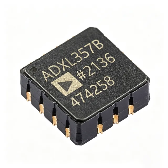
ADXL357BEZ - Low Noise 3-Axis MEMS Accelerometer | Analog Devices
The ADXL357BEZ is a low noise density, low 0 g offset drift, low power, 3-axis MEMS accelerometer from Analog Devices with selectable measurement ranges of ±10g, ±20g, and ±40g. It features a digital output via SPI or I2C interface and is housed in a 14-terminal CLCC package measuring 6mm x 6mm. The device operates over a bandwidth of 1 Hz to 1 kHz and is designed for high-performance industrial and instrumentation applications. An accelerometer is a sensor that measures proper acceleration, which is the rate of change of velocity of a body in its own instantaneous rest frame. MEMS (Micro-Electro-Mechanical Systems) accelerometers are micro-machined devices that integrate mechanical sensing elements with electronic circuitry on a single chip. They are widely used in motion sensing, vibration monitoring, and inertial navigation systems. The ADXL357BEZ belongs to the category of digital-output accelerometers, which convert the sensed acceleration into a digital signal for direct interfacing with microcontrollers or digital signal processors. Key features of the ADXL357BEZ include ultra-low noise density of 80 µg/√Hz, low 0 g offset drift of less than 0.75 mg over temperature, and low power consumption of 200 µA at 3.3 V. The device supports both SPI and I2C digital interfaces, allowing flexible integration into various system architectures. It also includes an integrated temperature sensor and a 32-level FIFO buffer to reduce host processor loading. The ADXL357BEZ utilizes a capacitive sensing element with a high-resolution sigma-delta ADC, providing excellent linearity and stability. The device is factory-calibrated for sensitivity and offset, minimizing the need for user calibration. Its low noise and low drift characteristics make it suitable for precision applications such as structural health monitoring, platform stabilization, and seismic sensing. Typical applications include industrial vibration monitoring, inertial measurement units (IMUs), robotics, and aerospace navigation systems. The device's wide measurement range and high bandwidth enable it to capture both low-frequency tilt and high-frequency vibration signals. Its low power consumption makes it ideal for battery-powered wireless sensor nodes. When designing with the ADXL357BEZ, ensure proper power supply decoupling with a 0.1 µF capacitor close to the VDD pin and a 1 µF capacitor on the VDD I/O pin. The device requires a supply voltage between 2.25 V and 3.6 V, and the digital interface voltage can be set independently via the VDD I/O pin. Careful PCB layout with a solid ground plane is recommended to minimize noise coupling.
ADXL357BEZ-RL - 3-Axis Digital Accelerometer | Analog Devices
The ADXL357BEZ-RL is a low noise density, low 0 g offset drift, low power, 3-axis accelerometer from Analog Devices with selectable measurement ranges of ±10g, ±20g, and ±40g. It provides digital output via SPI or I2C interface and is housed in a 14-lead CLCC (6mm x 6mm) package. The device operates over a bandwidth of 1Hz to 1kHz and is designed for high-performance industrial and instrumentation applications. An accelerometer is a sensor that measures proper acceleration, which is the rate of change of velocity per unit time. The ADXL357 is a MEMS capacitive accelerometer that converts mechanical displacement into an electrical signal, which is then digitized by an onboard ADC. It belongs to the category of inertial sensors, which are essential for motion detection, vibration monitoring, and tilt sensing. The ADXL357 family includes the analog output ADXL356 and the digital output ADXL357, with the ADXL357B variant supporting additional interface options. Key features of the ADXL357BEZ-RL include ultra-low noise density (typically 80 µg/√Hz), low 0 g offset drift over temperature, and low power consumption (typically 150 µA at 3.3V). The selectable measurement ranges allow the user to optimize resolution and dynamic range for specific applications. The device also includes an integrated temperature sensor and a 32-level FIFO buffer to reduce host processor loading. The ADXL357 uses a MEMS capacitive sensing element with a precision analog front-end and a 20-bit digital output. The device features a programmable high-pass filter and low-pass filter, enabling flexible signal conditioning. The SPI and I2C interfaces allow easy integration with microcontrollers and digital signal processors. The 14-lead CLCC package provides a compact footprint with excellent thermal and mechanical stability. Typical applications include structural health monitoring, condition monitoring of rotating machinery, inertial measurement units (IMUs), platform stabilization, and seismic sensing. The low noise and low drift characteristics make it suitable for precision tilt and vibration measurements. The wide bandwidth supports both static and dynamic acceleration measurements. When designing with the ADXL357BEZ-RL, ensure proper decoupling of the power supply and careful PCB layout to minimize noise coupling. The device requires an external pull-up resistor on the I2C lines if used in I2C mode. The FIFO can be configured to reduce interrupt overhead in high-sample-rate applications.