Sensoren
Unterkategorien
Produkte (525)

ATMXT3432S-S-CUR - maXTouch Touch Controller | Microchip
The Microchip Technology ATMXT3432S-S-CUR is a maXTouch mXT3432S capacitive touchscreen controller IC supplied as a Slave IC in a BGA package on tape and reel. The mXT3432S family is optimized for projected-capacitive touchscreens up to 17.3 inches and enables shieldless designs, reducing stack-up cost and module thickness. A projected-capacitive touch controller is a mixed-signal IC that drives excitation signals into a transparent ITO sensor grid, measures mutual-capacitance changes at each crossing node, and applies proprietary acquisition and filtering algorithms to report accurate touch coordinates to a host over I2C or SPI. Within the signal-chain hierarchy, it sits between the passive sensor stack and the host processor, functioning as the front-end of the human-machine-interface subsystem alongside display drivers and haptic ICs. Key features of the ATMXT3432S family include support for screens up to 17.3 inches, shieldless design operation that removes the need for a separate shield electrode, high signal-to-noise ratio acquisition hardware, wet-finger and gloved-touch performance, and Microchip's maXTouch feature set for superior responsiveness. The 'R' suffix in the ordering code denotes tape-and-reel delivery for automated SMT assembly, while the '-CUR' grading indicates the industrial operating grade. Technically, the device integrates analog front-end acquisition blocks, a digital signal processing core, and on-chip memory for configuration objects. The maXTouch object-based architecture allows designers to tune acquisition settings, touch thresholds, and gesture parameters through configuration objects rather than firmware rewrites. Typical applications include tablet and notebook touchscreens, industrial HMI panels, smart appliances, automotive-adjacent infotainment-adjacent displays, and point-of-sale terminals where medium-format capacitive touch is required without a shield layer. When designing with this part, validate the configuration object set against your specific sensor stack and cover-glass thickness, since shieldless operation is more sensitive to grounding and display-noise conditions. This page synthesizes distributor availability data, Microchip's official family positioning, recommended alternatives, and practical selection notes not consolidated in any single manufacturer datasheet.
ATMXT540SXES-CCUR - maXTouch 540-Ch Touch Controller | Microchip
The Microchip Technology (Atmel) ATMXT540SXES-CCUR is a maXTouch 540-channel projected-capacitive touchscreen controller IC from the maXTouch X series, supplied in bulk packaging. It belongs to the Atmel/Microchip maXTouch family of capacitive touch sensor ICs and provides mutual-capacitance touch acquisition for multi-touch human interface designs. A capacitive touchscreen controller is a type of sensor interface IC that scans a grid of transparent electrodes (ITO pattern) on a touch sensor, measures mutual capacitance changes caused by finger proximity, and reports processed touch coordinates to a host processor. Within the system hierarchy, the touchscreen controller sits between the touch sensor panel and the application host, forming part of the human-machine interface (HMI) subsystem alongside displays, buttons, and gesture engines. The ATMXT540SXES-CCUR is part of the maXTouch 540 series, engineered for multi-touch screens supporting standard touch and stylus use cases. Key family features typically include mutual-capacitance sensing, multi-touch reporting, noise-robust acquisition algorithms for charger and display noise immunity, and host communication over a serial interface (I2C/SPI per the maXTouch family convention). The '-CCUR' suffix denotes a specific pinout and packaging configuration in the XS pin-combination matrix of the maXTouch naming scheme. Architecturally, maXTouch devices integrate an acquisition engine with programmable scan frequencies and filtering that suppresses interference from LCD displays and switching chargers, allowing reliable touch operation in electrically noisy environments. The integrated touch processing offloads touch detection and tracking from the host CPU, reducing host software complexity and latency. Typical applications include smartphones, tablets, industrial HMI panels, automotive center-stack touchscreens, and smart appliance control surfaces where multi-touch capacitive sensing is required. Design consideration: touchscreen controller selection must match both the sensor electrode pattern (TX/RX channel count) and the mechanical stack-up; verify the exact channel matrix and interface before footprint commitment. Refer to the official Microchip maXTouch configuration tools for sensor tuning. This page synthesizes distributor availability, drop-in variant cross-references, and practical design guidance beyond the manufacturer datasheet.
ATMXT768E-CU - maXTouch 16-Touch Capacitive Touch IC | Microchip
The Microchip Technology ATMXT768E-CU is a maXTouch mXT768E-AT mutual-capacitance touchscreen controller IC supporting touchscreens up to 10.1 inch diagonal (and larger), with detection of up to 16 simultaneous touches, housed in a 96-ball VFBGA package. A capacitive touch controller is a specialized mixed-signal IC that drives transmit and receive electrodes on a touch sensor, measures mutual-capacitance changes at each node, and applies proprietary signal-processing algorithms to report finger, stylus, and gloved-touch coordinates to a host processor. Within the touch system hierarchy, it sits between the raw touch sensor (a patterned ITO or similar conductor on glass or film) and the host interface, forming the sensing layer of human-machine-interface (HMI) subsystems in embedded, industrial, and consumer designs. Key features include 16-touch simultaneous detection, support for shieldless single-layer sensor constructions that reduce stack-up cost and thickness, gloved-touch operation, and the maXTouch advanced touch-overlapping finger tracking for high-resolution, highly responsive operation on panels up to 10.1 inches or larger. The mXT768E-AT is part of Microchip's maXTouch E-series family, which integrates the acquisition engine and touch-processing firmware on-chip so the host receives processed touch reports rather than raw capacitance data. Technically, the device uses mutual-capacitance scanning with Microchip's maXTouch acquisition technology, performing self- and mutual-capacitance measurement cycles and on-chip filtering to reject display and charger noise. Configuration and calibration data are typically stored in an external EEPROM or the host flash and loaded at power-up over the I2C-compatible interface. Typical applications include industrial HMI touch panels, smart appliances, point-of-sale terminals, medical control panels, and larger-format embedded displays up to 10.1 inches and beyond. Design consideration: note that Microchip has designated the ATMXT1189TD-A as the recommended alternative touch controller, so new designs should evaluate this part and plan for lifecycle management. This page synthesizes distributor availability, the manufacturer-recommended replacement, and lifecycle guidance not consolidated in any single datasheet or distributor listing.
ATMXTS100-CUR - maXStylus Active Stylus ASIC | Microchip
The Microchip Technology ATMXTS100-CUR is a maXStylus Generation I active stylus ASIC, a capacitive touch sensor integrated circuit from the maXTouch family designed to drive and process signals for active electromagnetic-stylus touchscreen systems. It is supplied on Tape & Reel, carries ROHS3 compliant status, and is marketed as IC SENSOR MAXTOUCH in distributor catalogs. A capacitive touch sensor IC is a mixed-signal device that interfaces between a human-interface surface (touchscreen digitizer, stylus tip, or sensor electrode array) and a host processor. In the broader hierarchy of human-interface electronics, it sits within the touch and stylus controller category of interface and sensor ICs, converting analog capacitance or coupled-signal measurements into digitized position data. The maXStylus line was developed by Atmel, whose touch business was acquired by Microchip Technology, and the part is still referenced under both Atmel and Microchip brand names in distribution. The key differentiating feature of the maXStylus Gen I architecture is its purpose-built integration of stylus drive and sensing functions in a single ASIC, reducing the bill of materials for active-pen designs compared with discrete transmit/receive chains. Typical implementations pair this ASIC with a digitizer sensor stack and an I2C or SPI link to the host (exact interface details should be confirmed from the manufacturer datasheet). Typical applications include active stylus systems for tablets and e-notebooks, signature capture terminals, and pen-input industrial operator panels. Because the part is an ASIC for a specific stylus ecosystem, design-in is normally tied to Microchip maXStylus reference designs. A key design consideration is verifying ecosystem compatibility: active stylus protocols are generally not interchangeable between vendors, so second-sourcing typically requires requalification of the stylus and digitizer stack rather than a simple pin swap. This page synthesizes distributor stock data, compliance status, and sourcing context not consolidated in any single manufacturer or distributor listing. Pricing, package dimensions, and detailed electrical parameters marked as [DATA_NEEDED] should be confirmed against the official Microchip datasheet before design-in.
AWRL6844 - 57-64GHz Automotive mmWave Radar Sensor | Texas Instruments
The Texas Instruments AWRL6844 is a single-chip, high-performance, low-power 57GHz to 64GHz FMCW mmWave radar sensor designed for automotive in-cabin applications such as child presence detection, intrusion monitoring, and occupancy detection. It operates in the 57GHz to 63.9GHz band with up to 7GHz continuous chirp bandwidth and integrates a radar front-end, processing cores, and a Hardware Security Module (HSM). A mmWave radar sensor is a radar device that transmits and receives millimeter-wave electromagnetic signals (here 57 to 64GHz) and processes frequency-modulated continuous wave (FMCW) reflections to measure range, velocity, and angle of objects. Within the sensing hierarchy, it belongs to: radar sensor -> mmWave sensor -> integrated RF SoC -> semiconductor sensor device. The AWRL6844 belongs to the AWRL684x automotive family, alongside the related AWRL6843. Key features include the 57-64GHz band with 7GHz continuous chirp bandwidth for fine range resolution, an integrated Hardware Security Module (HSM) for secure in-cabin sensing, TI's low-power 45nm RF CMOS process enabling unprecedented integration in an extremely small form factor, and a compact 10.4 x 10.4 mm package suitable for hidden in-cabin mounting. The device is built for self-monitored, ultra-accurate radar systems in the automotive space. Technically, the AWRL6844 integrates a fully programmable radar front-end with an ARM Cortex-R4F processing core and hardware FFT acceleration on a single die, reducing BOM cost and board area versus discrete RF-plus-MCU solutions. Communication interfaces include CAN, I2C, LIN, SPI, and UART outputs (as seen on the AWRL6844DBGANCRQ1 device variant), enabling direct integration into vehicle body and domain controller networks. Typical applications include child presence detection (CPD) for Euro NCAP requirements, intrusion monitoring for anti-theft, occupancy detection for seatbelt and airbag logic, and gesture or vital-sign sensing inside the vehicle cabin. The 60GHz-class band and 7GHz bandwidth allow detection of micro-movements such as breathing even through seat covers. Design consideration: the AWRL6844 uses a different SDK and register/memory map than the earlier IWR6843, so migration requires software rework even where hardware function is similar. Plan for the MMWAVE L-SDK and Code Composer Studio device support packages early in development. Pricing and packaging details should be verified with TI or distributors as of 2026-08-29.
BA76220 - PIR Sensor Controller, 12µA Low Power, 1-Wire | Holtek
The Holtek BA76220 is a dedicated controller IC for human infrared (PIR) sensing applications, integrating a low-noise analog front-end (AFE) and a low-power digital control core in a single chip. According to the Holtek product page, it draws only 12µA quiescent current and supports 1-wire slave communication, which simplifies PCB routing and reduces wiring cost in multi-node sensor networks. The part provides multi-functional output control and is intended for high-sensitivity motion-detection end equipment such as automatic lighting, security alarms, and energy-saving occupancy switches. A PIR controller is a mixed-signal integrated circuit that interfaces directly with a pyroelectric infrared sensor and converts the small analog motion-induced voltage pulses into a digital trigger for downstream actuators. Within the broader system hierarchy, the BA76220 sits below the application layer (lighting, alarms) and above the sensor transducer, providing the analog conditioning, motion validation logic, and timing functions that a discrete op-amp + MCU solution would otherwise require. Holtek's product taxonomy places this part under PIR Controllers within their Touch/Proximity & Peripheral MCU family. Key features include the integrated 12µA AFE, 1-wire slave communication mode, an adjustable delay time platform covering 0.5s to 6h, and multi-functional output control. The integrated AFE eliminates external op-amp and filter components that designers would normally need to condition the PIR signal, while the 1-wire interface allows multiple BA76220 nodes to share a single data line back to a host MCU for centralized control. The adjustable delay platform covers common application timing from a few hundred milliseconds up to half a day, allowing a single SKU to serve both fast security loops and slow occupancy controls. Technically, the BA76220 combines a low-offset internal amplifier with on-chip threshold comparison and a programmable retriggerable monostable. The 12µA quiescent current is achieved through Holtek's low-power CMOS process and dynamic biasing of the AFE during active sensing windows. Designers configure delay time and sensitivity via simple external resistor selection, which keeps the BOM small and avoids any firmware development cycle. Typical applications include automatic LED lighting controlled by body motion, security alarm systems requiring high-sensitivity intrusion detection, smart home occupancy switches, and industrial energy-saving controls. The wide delay range (0.5s to 6h) makes it suitable for both short-cycle corridor lighting and long-cycle room occupancy applications. When designing with this part, use a proper Fresnel lens to focus IR onto the PIR sensor and place the sensor away from direct airflow sources. Avoid mounting the device near heat-generating components, as thermal gradients can cause false triggering even with proper compensation. This page synthesizes verified distributor data, drop-in alternative recommendations, and practical PCB design notes not found in the manufacturer datasheet alone, helping engineers select and implement the BA76220 with confidence.

CA+ - DS75S-CA+ Digital Temperature Sensor 11b | Analog Devices
The Analog Devices (formerly Maxim Integrated) DS75S-CA+ is a digital temperature sensor with a 9-bit to 12-bit (factory-default 11-bit) user-configurable resolution, an I2C/SMBus-compatible serial interface, and an operating range of -55 °C to +125 °C, packaged in an 8-pin SOIC (S) with the automotive-grade CA+ finish. The CA+ suffix is the vendor’s automotive/extended-quality screening designation applied on top of the base DS75S+ part, indicating the part meets stricter quality and reliability screening beyond the standard commercial grade. A digital temperature sensor is an IC that combines an on-chip bandgap or silicon-junction temperature transducer with an analog-to-digital converter (ADC) and a digital serial interface (commonly I2C, SMBus, or SPI). The sensor periodically samples die temperature, converts it to a calibrated digital word, and exposes the result over the bus, eliminating the need for external ADCs, op-amps, and linearization firmware. These devices sit in the hierarchy: temperature sensor → sensor IC → analog/mixed-signal IC → semiconductor, and they are widely used to replace discrete thermistors and thermocouples in system thermal-management designs. Key features of the DS75S-CA+ include ±2 °C (max) accuracy from -25 °C to +100 °C, ±3 °C accuracy over the full -55 °C to +125 °C range, a 2.7 V to 5.5 V supply range, an I2C/SMBus 2-wire interface supporting 9-bit to 12-bit resolution (with 11-bit factory default), three address pins allowing up to 8 devices on one bus, an overtemperature alarm output (O.S. pin) with user-programmable trip points, and a low 0.5 mA (typ) active supply current plus shutdown mode. The 8-pin SOIC footprint is hand-solder-friendly and compatible with virtually all 8-SOIC land patterns. Internally, the DS75S-CA+ uses an on-die bipolar-junction transducer whose delta-Vbe is digitized by a sigma-delta ADC and corrected in firmware by factory-trimmed coefficients stored in on-chip EEPROM. Each I2C transaction returns a signed two’s-complement temperature word; an integrated thermostat function compares the measurement against a programmable TOS/THYST window and asserts the open-drain O.S. pin to interrupt a host microcontroller without polling. Typical applications include automotive climate-control modules, server and networking thermal monitoring, white-goods and HVAC controllers, battery-pack thermal protection, and any embedded system that needs a board-level digital thermal alarm. The wide supply range (2.7 V to 5.5 V) and rugged -55 °C to +125 °C operating range make it equally suited to industrial and automotive environments. When designing with the DS75S-CA+, place a 0.1 µF decoupling capacitor within 5 mm of VDD and a 10 kΩ pull-up on the open-drain O.S. and SDA/SCL lines. Note that the CA+ suffix denotes extended-quality screening on top of the standard DS75S+ part; engineers verifying against the official datasheet should consult the device-specific ordering information table. This page synthesizes distributor pricing, drop-in alternatives, and practical design notes not found in the manufacturer datasheet.

CAP1126-1-AP-TR - 6-Channel Capacitive Touch Sensor, 2 LED Drivers | Microchip
The Microchip Technology CAP1126-1-AP-TR is a 6-channel capacitive touch sensor with two integrated LED drivers, housed in a 16-pin QFN (4x4 mm) package. Built on RightTouch® technology, it provides programmable sensitivity, automatic recalibration, and proximity detection for robust touch interfaces in noisy environments. A capacitive touch sensor is a solid-state device that detects the presence of a finger (or conductive object) by measuring the change in capacitance on an electrode. In the system hierarchy, the CAP1126 belongs to the capacitive sensor IC category, sitting above simple mechanical switches and below full touchscreen controllers. Compared with mechanical buttons, capacitive touch sensors offer sealed, aesthetically pleasing surfaces, no moving parts, and longer operational life, while still being lower complexity and lower cost than projected capacitive touchscreens. Key features include 6 independent capacitive touch inputs with programmable sensitivity, automatic recalibration to compensate for environmental drift, 2 LED drivers supporting on/off, variable-rate blinking, breathing, and dimming effects, an I2C/SMBus-compatible interface, and Multiple Pattern Touch recognition that reports simultaneous button presses as a distinct event. The integrated proximity-detection circuitry enables wake-on-approach operation, reducing system power consumption when no user is present. Technically, the CAP1126 uses a charge-transfer-based sigma-delta conversion technique for each sensor channel, providing high noise immunity against power-line and RF interference. Its automatic recalibration loop continuously adjusts the sensor baseline so that slow environmental changes (humidity, temperature) do not produce false triggers. The device operates from a single 3.0V to 3.6V rail, draws approximately 500 uA active supply current, and offers programmable interrupt signaling to the host MCU. Typical applications include consumer electronics front panels, white goods and appliance control surfaces, notebook and tablet button strips, industrial control keypads, and IoT devices requiring simple, sealed touch interfaces with visual LED feedback. The 2 integrated LED drivers directly drive indicator LEDs without external transistors. When designing with this device, ensure the touch sensor PCB pads are routed with adequate ground isolation and follow the Microchip Touch Sensor Design Guide layout recommendations. The I2C address is hardware-fixed on the -1 variant (0x28); verify bus conflicts with other peripherals on the same I2C bus. This page synthesizes distributor pricing, drop-in alternatives, and practical design notes not found in the manufacturer datasheet, providing unique value for both component selection and board bring-up.
CY8CMBR3002-SX1IT - 2-Button CapSense Express | Infineon
The Infineon CY8CMBR3002-SX1IT is a CAPSENSE MBR3 family capacitive touch button controller with 2 CapSense I/O channels, supplied in an 8-pin SOIC package with tape-and-reel packaging. It integrates Infineon's third-generation CSD PLUS (CapSense Sigma Delta Plus) sensing technology and provides a configurable 1.71 V to 5.5 V supply range with an operating temperature range of -40 °C to +85 °C, making it suitable for consumer, industrial, and appliance front-panel designs. A CapSense controller is a specialized mixed-signal IC that replaces mechanical buttons by detecting changes in capacitance caused by finger proximity or touch. Capacitive touch controllers sit within the broader category of human-machine interface (HMI) ICs, alongside touch-screen controllers, proximity sensors, and gesture-recognition devices. The CY8CMBR3002-SX1IT specifically targets simple button-only applications where ultra-low standby power, robust water-tolerance, and a minimal external BOM are more important than host MCU programmability. Key differentiating features include 2 CapSense I/O supporting up to 2 buttons, integrated SmartSense auto-tuning that eliminates manual CAPSENSE parameter calibration, an active-low mechanical replacement output (active-low when finger detected, active-high on release), I2C/SMBus configuration interface, low standby current optimized for battery-powered products, and an operating voltage range of 1.71 V to 5.5 V that covers 1.8 V, 3.3 V, and 5 V rails. The SOIC-8 footprint eases hand-soldering and rework compared to QFN alternatives. Architecturally, the CY8CMBR3002-SX1IT uses a Sigma-Delta ADC plus a proprietary CSD PLUS signal-processing pipeline to convert capacitive changes into digital button-state outputs. On-chip EEPROM-backed configuration registers allow designers to tune sensitivity, response time, and noise immunity through EzClick/I2C, eliminating firmware development and reducing time-to-market versus a programmable PSoC solution. Typical applications include replacement of mechanical buttons in white goods, kitchen appliances, and consumer electronics; touch keypads in audio devices and remote controls; rugged sealed keypads in industrial control panels; waterproof buttons for outdoor IoT devices; and low-power wake-up buttons in battery-powered smart-home sensors. The wide 1.71 V to 5.5 V range also supports single-cell Li-ion or 3 V coin-cell operation. When designing with the CY8CMBR3002-SX1IT, choose the external sense capacitor and PCB overlay geometry to balance sensitivity against water-film immunity. Power the device from a clean rail because noise on VDD directly translates into false-touch events, and place the device close to the sensors to keep the capacitive trace area small. This page synthesizes distributor pricing from LCSC and Octopart, cross-references pin-compatible Infineon MBR3 family alternatives, and packages practical design notes that are not consolidated in the manufacturer datasheet alone.
DMP320 - Precision Pressure Transmitter ≤0.5 ms Fast Response | BD|SENSORS
The BD|SENSORS DMP320 is a precision pressure transmitter with a sub-millisecond response time (≤0.5 ms) and a 10 kHz sampling rate, engineered for high-speed dynamic pressure measurement. Housed in a stainless-steel sensor body, the DMP320 covers nominal pressure ranges from 0…100 mbar up to 0…600 bar and outputs a standard analog signal for direct interface with industrial controllers and data-acquisition systems. What is a pressure transmitter? A pressure transmitter is an industrial sensor that converts an applied pressure into a standardized electrical output (commonly 4–20 mA, 0–10 V, or a digital bus signal). Within the sensor hierarchy, the DMP320 sits in the precision-and-dynamic-measurement category, above static process transmitters and below research-grade pressure scanners. Its high-speed signal chain allows pressure curves, peaks, and hydraulic spikes to be recorded with high fidelity, which sets it apart from slower industrial loop-powered devices. Key features of the DMP320 include: ≤0.5 ms response time enabling capture of transient pressure events; 10 kHz internal sampling rate for fine-grained waveform reconstruction; wide pressure envelope (0…100 mbar to 0…600 bar) for both vacuum and high-pressure service; stainless-steel wetted parts for media compatibility; digital signal processing of the sensor signal by newly developed electronics; and configurable output suitable for industrial automation. Architecturally, the DMP320 uses a piezoresistive or thin-film stainless-steel measuring cell whose millivolt output is digitized and conditioned by a digital electronics module. The 10 kHz oversampling paired with sub-millisecond analog output update allows the device to track pressure peaks that conventional 1–2 Hz process transmitters miss entirely. This combination is critical for hydraulic testing, fuel-injection diagnostics, and dynamic pressure profiling. Typical applications include fast hydraulic pressure monitoring in test rigs and mobile hydraulics, peak pressure detection in fuel-injection and combustion test benches, dynamic profiling of HVAC/R and process pressures, and laboratory instrumentation where pressure curves, peaks, and hits must be measured exactly. The stainless-steel construction also supports chemically aggressive media under the medium temperature envelope. When designing with the DMP320, observe the medium temperature limits (typically -40 to 125 °C depending on version) and the electronics operating temperature range; derate the mounting configuration accordingly. Never insert pointed tools or direct compressed-air jets against the sensitive measuring diaphragm, as permanent deformation of the diaphragm will permanently corrupt calibration and accuracy. Verify cable gland sealing for the installation environment. This page synthesizes distributor availability, drop-in equivalents in the BD|SENSORS precision-transmitter family, and practical mounting guidance not found in the standalone datasheet, giving engineers a single source for sourcing and selecting the DMP320.

DS18B20+ - 1-Wire Digital Thermometer, 9-12 bit, TO-92-3 | Maxim
The Maxim Integrated (Analog Devices) DS18B20+ is a 1-Wire digital thermometer providing programmable 9-bit to 12-bit Celsius temperature measurements with nonvolatile user-programmable upper and lower alarm trigger points, housed in a 3-pin TO-92-3 package. The part features a measurement range of -55C to +125C with +/-0.5C accuracy from -10C to +85C and a maximum 750 ms conversion time at 12-bit resolution. A digital temperature sensor is an integrated transducer that converts a physical temperature into a calibrated digital word via an on-die bandgap reference, sigma-delta ADC, and serial protocol engine. The DS18B20 sits in the product taxonomy of: temperature sensor -> digital temperature sensor -> thermal sensor -> sensor IC -> semiconductor. It uses Maxim's 1-Wire protocol, a single-wire half-duplex serial bus that requires only one data line plus ground for communication with a host microcontroller, and supports multi-drop networking of many DS18B20 devices on the same wire through unique 64-bit ROM IDs. Key features include an operating voltage range of 3.0 V to 5.5 V (external power mode) or 3.0 V to 5.5 V with parasite-power support derived from the data line, four programmable resolution steps (9, 10, 11, 12 bit corresponding to 0.5C, 0.25C, 0.125C, 0.0625C LSB), and on-die EEPROM that retains user alarm thresholds across power cycles. The TO-92-3 through-hole package simplifies breadboard and hand-wired prototype use, while the SO-8 and uSOP variants (DS18B20Z, DS18B20U) target surface-mount designs. The device incorporates a 64-bit factory-lasered ROM containing a unique serial number, an on-die temperature sensor with internal signal conditioning, nonvolatile EEPROM for alarm TH and TL plus configuration register, and a power-on detect circuit. The DS18B20 returns temperature as a 16-bit two's-complement value over the 1-Wire bus with strict CRC-8 protection on every transaction, eliminating bit errors in electrically noisy environments. Typical applications include HVAC environmental monitoring, building automation, server-rack cold-aisle telemetry, industrial process monitoring, and IoT weather stations. The DS18B20 is widely used in Arduino, ESP32, and Raspberry Pi projects where multiple sensors share one GPIO pin, providing low-cost, cable-friendly distributed sensing. Stainless-steel waterproof probe assemblies based on the DS18B20 are the de facto standard for liquid and soil temperature measurement. When designing with the DS18B20+, ensure the data line has a 4.7 kohm pull-up to VDD and that long cable runs use STP/UTP with ground to limit ringing; parasite-power mode requires a strong pull-up during conversion. Decouple VDD with 100 nF close to the pin in externally powered mode. This page synthesizes distributor pricing, drop-in alternatives, and practical design notes that go beyond the datasheet's pin table.
EP0L001 - IO-Link Master Multiprotocol PROFINET/EtherNet/IP | wenglor
The wenglor EP0L001 is an IO-Link Master Multiprotocol that provides seamless integration of IO-Link sensors and standard digital sensors into PROFINET and EtherNet/IP industrial Ethernet networks. Housed in a rugged zinc diecast enclosure with IP65/IP67/IP69K ingress protection, it is engineered for harsh industrial environments where standard cabinet-mounted masters would fail. The unit acts as a gateway between field-level IO-Link devices and higher-level PLC or SCADA controllers, supporting standard digital I/O channels alongside IO-Link v1.1 communication. An IO-Link Master is a network device that sits at the boundary between a digital industrial sensor (IO-Link device) and a higher-level fieldbus or Industrial Ethernet backbone such as PROFINET, EtherNet/IP, or EtherCAT. IO-Link itself is a point-to-point, low-level digital communication standard (IEC 61131-9) that replaces traditional analog 4-20 mA and discrete switching signals with bidirectional, parameterizable digital channels. The master orchestrates communication, exchanges process data, and provides diagnostic feedback to the controller, making it a fundamental building block in Industry 4.0 sensor-to-cloud architectures. Key features of the EP0L001 include multiprotocol support for PROFINET and EtherNet/IP on a single hardware platform, IP65/IP67/IP69K protection rating for washdown and outdoor zones, and a zinc diecast housing that resists mechanical impact, oils, and coolants. The device typically offers multiple IO-Link ports (4 or 8) plus dedicated standard digital inputs, enabling mixed sensor topologies. Configuration is managed via web server, TIA portal, or wenglor's UniVision software, eliminating the need for proprietary programming tools. Technically, the EP0L001 implements the IO-Link v1.1 specification with full COM1/COM2/COM3 baud rates, supports SIO (Standard IO) fallback mode on each port, and provides per-port diagnostic data including voltage, current, and temperature monitoring. The dual-protocol firmware uses a dynamic selection mechanism that detects the controller's protocol on startup, allowing installers to deploy the same part across mixed PLC fleets without hardware swaps. Typical applications include automotive body-in-white welding lines, food and beverage bottling under hygienic washdown conditions, machine tool spindles requiring coolants resistance, and outdoor conveyor systems in logistics yards. System integrators select the EP0L001 when standard IP20 masters cannot survive the ambient conditions, and when both PROFINET and EtherNet/IP must coexist within a single facility. When designing with this device, plan for a 24 VDC Class 2 power supply with adequate headroom for port current, mount the unit vertically to allow drainage of any condensation, and verify M12 connector pinout against the wenglor datasheet before field installation. Most importantly, validate cycle time budgets against the controller's IO-Link call interval to ensure deterministic process data delivery. This page synthesizes distributor pricing from Standard Electric Supply and motionworld, practical design notes not found in the marketing datasheet, and an honest comparison against equivalent masters from Balluff, Sick, and Turck to help engineers select the right field-mountable IO-Link master for harsh-environment installations.
HDC1080DMBR - ±2% RH Low-Power Digital Humidity & Temp Sensor | TI
The Texas Instruments HDC1080DMBR is a digital humidity and temperature sensor with integrated signal conditioning that provides ±2% RH typical relative-humidity accuracy and ±0.2°C typical temperature accuracy, factory calibrated, in a 6-pin WSON (DMB) surface-mount package. The device communicates over I2C (Fast Mode up to 400 kHz) and supports 14-bit measurement resolution, with a 100 nA sleep-mode current and an average supply current of 710 nA at 1 sample/second (11-bit RH). A humidity sensor is a transducer that converts the water-vapor content of ambient air into a quantifiable electrical signal. Digital humidity sensors integrate the sensing element, analog front-end, sigma-delta ADC, and calibration memory into a single IC, exposing a digital bus interface (typically I2C) for the host microcontroller. The HDC1080 belongs to the capacitive polymer humidity-sensor family, which sits within the broader class of MEMS environmental sensors and ultimately within the sensor and signal-conditioning IC hierarchy used in modern embedded designs. Key features include a wide supply range of 2.7V to 5.5V, on-chip heater for self-dehumidification, and excellent stability at high humidity thanks to a PTFE (polytetrafluoroethylene) hydrophobic membrane option. The integrated temperature sensor eliminates the need for a separate thermistor or external RTD, reducing BOM count and PCB area. A programmable measurement sequence lets the host read humidity-only, temperature-only, or both in a single I2C transaction. From an architectural standpoint, the HDC1080 uses a parallel capacitive polymer die and a precision bandgap-referenced temperature sensor, multiplexed into a single 14-bit sigma-delta ADC. Factory calibration coefficients stored in on-chip OTP memory are applied automatically, removing per-unit two-point calibration from the user's manufacturing flow and improving unit-to-unit consistency. Typical applications include battery-powered IoT environmental monitors, HVAC indoor-air-quality sensors, smart thermostats, respiratory/CPAP humidifier feedback, refrigerator and freezer dew-point control, and asset-tracking cold-chain loggers. The 100 nA sleep current makes the part especially attractive for energy-harvesting and coin-cell nodes where average system current must remain in the low microamp range. When designing with this device, place a 0.1 µF decoupling capacitor within 5 mm of VDD and avoid running I2C clock/data traces parallel to switching-node traces; exposed backside pad must be soldered to the ground pour for thermal and mechanical integrity. This page synthesizes distributor pricing, verified drop-in alternatives, and practical design notes not found in the manufacturer datasheet alone.
HSFPAR003A - Piezoresistive Force Sensor, SMD | Alps Alpine
The Alps Alpine HSFPAR003A is a surface-mount piezoresistive force sensor from the HSFPAR series, designed for high-sensitivity load detection and depth-of-water detection in a compact SMD package. The device integrates a piezoresistive bridge circuit formed on a silicon diaphragm, achieving higher linearity than polymer or foil-based force sensors, and is supplied on Tape & Reel for automated assembly. According to the Alps Alpine product page, this part is intended for load detection and water-depth sensing applications. A force sensor (also called a load cell or pressure sensor in this category) is a transducer that converts an applied mechanical force or pressure into a quantifiable electrical signal. Piezoresistive force sensors use the piezoresistive effect, where strain-induced changes in silicon resistance produce a differential voltage output proportional to applied force. Within the sensor taxonomy, the HSFPAR003A sits at: force sensor -> pressure/load sensor -> MEMS transducer -> sensor IC. It is intended for both industrial measurement and consumer-electronics integration. Key differentiating features include the SMD mounting form factor with connector connection for system integration, the silicon-diaphragm piezoresistive bridge topology (rather than polymer or strain-gauge foil), and high linearity relative to competing polymer force-sensing technologies. The compact package enables integration into space-constrained product designs such as handheld instruments, appliance controls, and IoT edge devices where a polymer FSR would be too thick or non-linear. Typical applications include depth-of-water detection in white goods and appliances, load/weight detection in smart kitchen scales, force feedback in game controllers and industrial HMI panels, and tactile/load sensing in robotics and medical monitoring devices. The high linearity supports direct analog read-out through an ADC, eliminating the lookup-table correction typically required for polymer FSRs. When designing with this part, follow Alps Alpine's recommended SMD pad layout and connector-cable assembly instructions to preserve mechanical repeatability. Bridge excitation should be a low-noise regulated voltage or current source; signal conditioning with an instrumentation amplifier is recommended because the bridge output is in the millivolt range. This page synthesizes distributor pricing, pin/connector reference, drop-in alternatives, and practical design notes not found in the manufacturer datasheet alone. Pricing references reflect distributor data as of 2026-10-14.
HSFPAR303A - Silicon Diaphragm Force Sensor 4x4mm | Alps Alpine
The Alps Alpine HSFPAR303A is a silicon-diaphragm piezo-resistive force sensor unit housed in a compact 4.0 mm x 4.0 mm x 1.6 mm surface-mount package. It integrates a Wheatstone bridge circuit formed directly on the silicon diaphragm, so that applying force to the top of the diaphragm unbalances the bridge and produces a differential analog output voltage proportional to the applied load. A force sensor (also called a load cell or force-sensing resistor at higher force ranges) is a transducer that converts mechanical force into a measurable electrical signal. Force sensors sit inside the broader sensor hierarchy of pressure sensors -> load sensors -> mechanical-quantity sensors -> transducers, and are widely used for touch, weight, and tactile-feedback applications where a strain gauge, load cell, or piezo-resistive element is required. Key features include high-sensitivity load detection with low temperature drift, a small 4 mm footprint that enables dense PCB arrays, and an analog ratiometric output that interfaces directly with an external ADC or op-amp signal conditioner. The piezo-resistive silicon diaphragm delivers fast mechanical response and excellent repeatability compared with polymer-based FSRs. The HSFPAR303A uses a diffused piezo-resistive bridge on a micromachined silicon diaphragm. When force is applied, the diaphragm flexes and the bridge resistors change value, producing a differential output. This monolithic construction gives the part better long-term stability and lower part-to-part variation than discrete strain-gauge assemblies. Typical applications include stylus tip-force detection in pen tablets, key-press force measurement in industrial keypads, robotic gripper load feedback, precision weighing scales, and tactile/force-feedback switches in medical and consumer electronics. The compact package also suits wearable devices where PCB area is constrained. When designing with this part, treat the analog output as a low-level signal and use a low-noise, low-offset instrumentation amplifier or 16-bit ADC front-end. Apply force only along the designed axis and respect the datasheet-specified maximum force rating to avoid permanent deformation of the silicon diaphragm. This page synthesizes Mouser and Octopart pricing tiers, Alps Alpine datasheet parameters, and practical signal-conditioning notes not found in the manufacturer datasheet PDF alone.
HSPPAD042A - 300-1100 hPa I2C MEMS Pressure Sensor | Alps Alpine
The Alps Alpine HSPPAD042A is a digital MEMS barometric pressure sensor operating from 300 hPa to 1100 hPa with an I2C interface, housed in a compact SMD-10P package measuring 2 x 2.5 mm. The device runs on a single supply of 1.7 V to 3.6 V and draws only 1.8 uA typical supply current, making it well-suited for battery-powered portable designs. A digital pressure sensor is an electronic component that converts absolute gas pressure into a calibrated digital output via an integrated MEMS sensing element and an on-chip analog front-end plus ADC. Pressure sensors sit within the broader transducer hierarchy: transducer -> sensor -> pressure sensor -> barometric/absolute pressure sensor -> board-mount pressure sensor. The HSPPAD042A specifically targets barometric pressure measurement, the same form of pressure used in weather forecasting and altitude estimation, where the sensor measures pressure relative to an internal vacuum reference. Key features of the HSPPAD042A include a Philips I2C-BUS Specification v2.1 / NXP UM10204 Rev.03 compliant slave interface at fixed address 1001000x (Write:0, Read:1), an operating temperature range of -40C to +85C, and a RoHS-compliant surface-mount package. The part targets mobile, wearable, and IoT designs that require accurate barometric readings without the layout burden of an analog front-end. Pressure resolution and conversion timing are controlled via the I2C interface, allowing the host MCU to manage power consumption by issuing one-shot conversions. Typical applications include barometric altitude estimation in drones and wearables, weather station modules, HVAC air-flow monitoring, indoor navigation pressure references, and altitude-aware GPS augmentation in smartphones. The 1.8 uA quiescent current allows years of operation on a coin cell when paired with duty-cycled wake-up, while the small 2 x 2.5 mm SMD-10P footprint allows direct integration on dense IoT boards. When designing with this sensor, place decoupling capacitors (typically 100 nF ceramic) as close as possible to the VDD pin and route the I2C SDA/SCL traces as short as possible with pull-up resistors in the 2.2 kOhm to 10 kOhm range. Avoid placing the sensor directly over heat-generating components, as thermal gradients introduce pressure offset errors. According to the Alps Alpine datasheet, the I2C slave address is fixed at 0x48 (Write) / 0x49 (Read) and the bus supports standard and fast modes per NXP UM10204. This page synthesizes distributor pricing from LCSC and Mouser, drop-in alternatives from same-family Alps Alpine pressure sensors, and practical design notes not aggregated on the manufacturer product page. Engineers evaluating barometric sensor options will find parametric comparisons and design considerations specific to the HSPPAD042A here.
HSPPAD132A - Waterproof MEMS Absolute Pressure Sensor | ALPSALPINE
The ALPSALPINE HSPPAD132A is a compact, waterproof MEMS digital pressure sensor from the HSPPAD Series, delivering absolute pressure measurements from 4.35 PSI to 15.95 PSI (30 kPa to 110 kPa) and atmospheric / water-depth detection for low-power IoT and wearable designs. It outputs 16-bit pressure data over a digital I2C-compatible interface and ships in a surface-mount module package rated for waterproof assemblies with gel protection on the sensing element. What is a digital pressure sensor? A digital pressure sensor is a MEMS (Micro-Electro-Mechanical Systems) transducer that converts an applied pressure into an electrical signal, then conditions and digitizes that signal inside the same package to produce a digital output (I2C, SPI, or similar). It belongs to the broader sensor category under electronic components, sits above raw analog sensors in the hierarchy (sensor -> pressure sensor -> absolute pressure sensor -> digital pressure sensor -> MEMS pressure sensor), and is widely used in consumer wearables, mobile devices, weather stations, and depth-of-water detection. The digital output eliminates external ADC design effort and reduces MCU load via the standard I2C/SPI protocol. Key features of the HSPPAD132A include an absolute pressure range of 30 kPa to 110 kPa (4.35 PSI to 15.95 PSI), 16-bit pressure resolution, an integrated I2C digital interface, surface-mount packaging, and an operating profile tuned for low-power handheld products. The waterproof gel-coated sensing element resists direct water exposure that would otherwise damage conventional MEMS dies, making the part uniquely suited to outdoor wearables, sports watches, and depth-sensing applications. The sensor includes internal signal conditioning and calibration data stored in on-chip memory, allowing the host MCU to retrieve compensated pressure readings without external compensation circuitry. From an architectural standpoint, the HSPPAD132A uses a piezoresistive MEMS membrane coupled to a mixed-signal ASIC that performs amplification, temperature compensation, and ADC conversion. Its 16-bit output delivers pressure resolution suitable for 0.01 kPa-class applications such as barometric altitude sensing. Internal calibration coefficients are typically applied in software on the host side to correct for temperature and part-to-part variation. Typical applications include barometric altitude measurement in sports watches and fitness bands, atmospheric pressure trend monitoring in weather stations, water-depth detection in pool/swim sensors, drone altitude hold, and HVAC pressure monitoring. Industrial use cases include compressed-air line pressure trending and gas-meter pressure measurement where waterproofing is a plus. When designing with this sensor, place the device at the edge of the board near the waterproof vent/port to minimize the air-path length to the diaphragm, and route the I2C lines away from switching power and high-frequency signals. Decouple VDD with at least 0.1 µF ceramic close to the supply pin, and observe the I2C pull-up sizing guidance from the manufacturer datasheet for the chosen bus speed. This page synthesizes datasheet specifications, distributor pricing as of 2026-10-14, drop-in alternative notes, and practical design guidance not found in the standalone manufacturer datasheet, providing a one-stop reference for engineers evaluating the HSPPAD132A.
HSPPAR003D - 50-110 kPa Absolute Pressure Sensor | Alps Alpine
The Alps Alpine HSPPAR003D is an absolute-pressure MEMS sensor in a 2.5 x 2.5 mm 4-pin SMD package, delivering a ratiometric analog output proportional to absolute pressure over a 50 kPa to 110 kPa range (7.25 to 15.95 psi). Designed for atmospheric-pressure detection, the device provides a calibrated analog voltage output with ±1% FS accuracy over a -20 °C to +85 °C operating window. The miniature 4-SMD, no-lead footprint suits space-constrained consumer, industrial, and IoT designs. An absolute pressure sensor is a transducer that measures pressure relative to a perfect vacuum (zero reference), unlike gauge sensors that measure relative to ambient atmospheric pressure. In the broader sensor hierarchy, the HSPPAR003D belongs to the MEMS (micro-electro-mechanical systems) pressure-sensor family, which sits inside the pressure sensors / transducers category and ultimately under measurement sensors. Absolute-pressure sensors are preferred when the design must resolve altitude change, sealed-cavity pressure, or weather-related barometric variation independent of local atmospheric drift. Key features of the HSPPAR003D include ±1% FS accuracy, a wide 50-110 kPa pressure range that fully covers the barometric 100 kPa nominal point, surface-mount construction for reflow-compatible assembly, and an analog ratiometric output that scales with the supply voltage for direct ADC interfacing. The 4-lead no-lead SMD package simplifies PCB layout while keeping the part compatible with automated pick-and-place lines. The sensor uses a piezoresistive MEMS die coupled with a signal-conditioning ASIC that performs offset, span, and temperature compensation. Internal calibration data stored on-die allows the part to deliver a factory-trimmed analog transfer function, removing the need for external compensation components on the application board. Typical applications include portable weather stations, altimeters for wearable and handheld devices, HVAC system pressure monitoring, IoT environmental nodes, and indoor air-quality instruments. The 50-110 kPa window is well aligned with the barometric pressure band (approximately 87-108 kPa at sea level to alpine elevations). Design tip: route the supply and output traces as a differential pair when the sensor sits more than 25 mm from the ADC; long single-ended traces pick up switcher noise that directly modulates the analog output. Add a 100 nF decoupling capacitor within 5 mm of the supply pin. This page synthesizes distributor pricing, drop-in alternatives, and practical board-level design notes not found in the manufacturer datasheet alone.
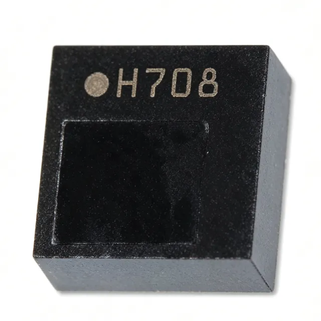
HTS221 - Capacitive Digital Humidity & Temperature Sensor | STMicroelectronics
The STMicroelectronics HTS221 is a compact, ultra-low-power capacitive digital humidity and temperature sensor designed for a wide range of applications including IoT, wearables, and environmental monitoring. It integrates a sensing element, analog front-end, and a 16-bit ADC in a single 2.0 x 2.0 x 0.9 mm HLGA package, providing accurate relative humidity and temperature measurements with minimal power consumption. A humidity and temperature sensor is a device that measures the amount of water vapor in the air and the ambient temperature, converting these physical quantities into digital signals for processing. In the system hierarchy, the HTS221 is a MEMS sensor that falls under the category of environmental sensors, which are part of the broader sensor family used in IoT, automotive, and industrial applications. Its role is to provide real-time environmental data that enables smart systems to react to changes in humidity and temperature. Key features of the HTS221 include a relative humidity accuracy of ±3.5% RH (20-80% RH), a temperature accuracy of ±0.5 °C (15-40 °C), and a humidity resolution of 0.004% RH. The sensor operates from a 1.7V to 3.6V supply, with a typical current consumption of 2 µA at 1 Hz output data rate, making it ideal for battery-powered devices. It communicates via I2C and SPI interfaces, and includes a programmable interrupt output for threshold detection. The HTS221 uses a capacitive sensing principle, where a polymer dielectric absorbs water vapor, changing the capacitance of the sensing element. This change is converted to a digital signal by a 16-bit ADC, providing high resolution and stability. The sensor also features an embedded heater for dew point measurement and condensation prevention, enhancing its versatility in demanding environments. Typical applications include smart home thermostats, HVAC systems, weather stations, and wearable health monitors. In smart thermostats, the HTS221 provides accurate humidity and temperature data to optimize comfort and energy efficiency. In wearables, its low power consumption extends battery life while enabling continuous environmental monitoring. When designing with the HTS221, ensure proper PCB layout with a clean ground plane and adequate decoupling capacitors (100 nF) near the VDD pin. The sensor should be placed away from heat sources and direct airflow to avoid measurement errors. For best performance, follow the recommended soldering profile and reflow conditions specified in the datasheet.
HTS221TR - Capacitive Digital Humidity & Temperature Sensor | STMicroelectronics
The HTS221TR is a compact, ultra-low-power capacitive digital humidity and temperature sensor from STMicroelectronics, packaged in a 3x3x0.9 mm HLGA (HLGA-6L) package. It integrates a sensing element and a mixed-signal interface, providing calibrated digital output over an I2C or SPI interface. The sensor measures relative humidity from 0% to 100% RH with an accuracy of ±3.5% RH (20-80% RH) and temperature from -40°C to +120°C with an accuracy of ±0.5°C (15-40°C). It operates from a 1.7V to 3.6V supply, drawing only 2 µA at 1 Hz sampling rate, making it ideal for battery-powered applications. A humidity sensor is a device that measures the amount of water vapor in the air, typically expressed as relative humidity (RH). The HTS221TR is a capacitive-type sensor, where the dielectric constant of a polymer layer changes with humidity, altering the capacitance of the sensing element. This change is converted to a digital signal via an internal ADC. In the broader system hierarchy, the HTS221TR is a MEMS environmental sensor, falling under the category of sensors, specifically temperature and humidity sensors, which are essential components in IoT, smart home, and industrial monitoring systems. Key features of the HTS221TR include its factory-calibrated output, eliminating the need for user calibration, and its programmable interrupt outputs for threshold detection. The sensor supports both I2C (up to 400 kHz) and SPI (up to 10 MHz) interfaces, providing flexibility in system integration. It also features a 16-bit resolution for both humidity and temperature, with a humidity resolution of 0.004% RH and temperature resolution of 0.01°C. The device includes an embedded heater for condensation prevention, which is useful in high-humidity environments. Technically, the HTS221TR uses a MEMS capacitive sensing element with a dedicated ASIC for signal conditioning. The sensor's low power consumption (2 µA at 1 Hz) and wide supply voltage range (1.7V to 3.6V) make it suitable for portable and wearable devices. The HLGA package is designed for surface mounting, with a small footprint of 3x3 mm, enabling compact PCB designs. The sensor's response time is typically 8 seconds for humidity and 5 seconds for temperature, ensuring real-time monitoring capabilities. Typical applications include smart home climate control, where the sensor monitors indoor humidity and temperature to optimize HVAC systems; industrial environmental monitoring, where it tracks conditions in warehouses or server rooms; and wearable devices, where it measures skin humidity and ambient temperature for health tracking. The sensor's accuracy and low power make it ideal for battery-operated IoT nodes. When designing with the HTS221TR, ensure proper PCB layout to minimize the influence of heat sources on temperature readings. Place the sensor away from components that generate heat, and provide adequate ventilation for humidity sensing. The sensor's I2C address is 0x5F, and it supports multiple devices on the same bus with different addresses.
HUS723030ALS640 - 3TB 7.2K SAS 6Gb/s Enterprise HDD | HGST Ultrastar 7K3000
The HGST Ultrastar 7K3000 HUS723030ALS640 is a 3 TB enterprise-class 3.5-inch hard disk drive spinning at 7,200 RPM with a SAS 6 Gb/s interface, 64 MB cache buffer, and the legacy 512n (native) sector format. Designed for 24x7 datacenter and RAID array workloads, it shares the seventh-generation 5-platter mechanical platform introduced by Hitachi (now Western Digital / HGST). The drive is rated at 2.0 million hours MTBF and is targeted at bulk-capacity storage tiers, secondary backup arrays, and entry-level enterprise rack enclosures where cost-per-TB outweighs raw IOPS. A 3.5-inch enterprise HDD is a rotational magnetic storage device built around stacked aluminum platters, a high-speed spindle motor, and a multi-head actuator that delivers sequential and random access on a SATA or SAS transport. Within the broader storage taxonomy, the HUS723030ALS640 sits in the capacity-optimized segment of enterprise HDDs, below 10K/15K RPM performance HDDs and well below SSDs on the IOPS axis, but ahead of nearline-SATA drives on the interface reliability and dual-port fault-tolerance axis because SAS supports full-duplex dual-port operation. It is the workhorse building block of the Ultrastar 7K3000 family, and the suffix "A L S 6 4" decodes as Ultrastar-generation / large-form-factor / 512n sector / SAS 6 Gb/s / 64 MB cache. Key specifications include sustained sequential read throughput of approximately 184 MB/s, sustained sequential write of roughly 200 MB/s, an average seek time near 8.2 ms, dual-port SAS connectivity, and a 2.0 million hour MTBF rating backed by a 5-year limited warranty. The drive also provides Rotational Vibration (RV) sensor technology for use in dense multi-drive chassis, Power Choice power management to reduce idle watts, and TLER / ERC (time-limited error recovery) to behave predictably inside RAID rebuilds. Architecturally, the HUS723030ALS640 uses a 6 Gb/s SAS PHY with an 8B/10B encoded serial transport, a 64 MB DRAM read/write cache, and on-the-fly ECC across the recording channel. Its 5-platter, 10-head mechanical design delivers the 3 TB raw capacity, while its rotational speed and cache tuning target sequential workloads over random-IO micro-transactions. Typical applications include enterprise backup targets, secondary storage tiers in software-defined storage, cold-data archival within hyperscale datacenters, surveillance/NVR bulk storage with sustained write streams, and capacity-tier nodes in scale-out object storage clusters. The 3 TB capacity point is also widely deployed as a Dell PowerEdge / Compellent FRU and as an Oracle / Sun / Cisco spare. When designing systems around this drive, ensure the HBA or RAID controller supports 512n sector emulation (older controllers may default to 512e-only mode). Validate TLER behaviour matches the rest of the array to avoid spurious RAID dropouts, and provision airflow of at least 5 CFM per drive in dense enclosures to keep the ambient below 35 degrees Celsius. This page synthesizes distributor pricing, sibling variant listings, pinout and interface notes, and practical design considerations not found in the manufacturer datasheet alone, giving procurement and datacenter engineers an at-a-glance decision resource.

ICM-20689 - 6-Axis IMU, DMP, ±32g Accel | TDK InvenSense
The TDK InvenSense ICM-20689 is a high-performance 6-axis MotionTracking device that combines a 3-axis gyroscope, a 3-axis accelerometer, and an embedded Digital Motion Processor (DMP) in a compact 4 mm x 4 mm x 0.9 mm 24-pin QFN package. According to the TDK datasheet, it supports a wide VDD range of 1.71 V to 3.45 V, accelerometer full-scale ranges up to ±32 g, and gyroscope full-scale ranges up to ±2000 dps, with I²C, SPI, and auxiliary I²C interfaces. An Inertial Measurement Unit (IMU) is a sensor module that measures specific force, angular rate, and - in 6-axis variants - orientation via a 3-axis gyroscope and 3-axis accelerometer. IMUs belong to the broader category of MEMS motion sensors and are core elements in inertial navigation, gesture recognition, and stabilization. They sit at the bottom of a hierarchy that runs: IMU -> motion sensor -> MEMS sensor -> semiconductor. The ICM-20689 integrates an on-chip DMP that offloads motion-processing algorithms from the host MCU, reducing system power and enabling sensor fusion at the edge. Key features include a 4-Kbyte FIFO that reduces host-processor wakeups, low-noise gyro bias stability, factory-calibrated scale factors, and an AP_AD5 auxiliary master I²C interface for connecting external sensors such as magnetometers. Programmable interrupts, self-test routines, and wake-on-motion thresholds simplify host integration. An on-chip temperature sensor with digital output is also provided for compensation. Typical applications span consumer drones, VR/AR headsets, robotics, wearable sports devices, IoT edge sensors, and gaming controllers, where the DMP handles gesture fusion and pedometer functions without burdening the application processor. Industrial variants leverage the same hardware platform for asset tracking, platform stabilization, and dead-reckoning assistance.
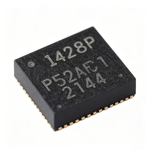
ICM-42688-P - 6-Axis MEMS IMU with 2KB FIFO | TDK InvenSense
The TDK InvenSense ICM-42688-P is a high-precision 6-axis MEMS MotionTracking device that integrates a 3-axis gyroscope and a 3-axis accelerometer in a compact 2.5 x 3.0 x 0.91 mm 14-pin LGA package. It supports I3C, I2C, and SPI serial interfaces, features a 2 kB FIFO, and offers ultralow-power wake-on-motion support to minimize system power consumption. The device is designed for a wide range of motion sensing applications, including drones, robotics, AR/VR, and industrial monitoring. An IMU (Inertial Measurement Unit) is a sensor that measures angular rate and linear acceleration using gyroscopes and accelerometers. The ICM-42688-P combines these into a single package, providing high accuracy and low noise for motion tracking. IMUs are essential in applications requiring orientation and movement detection, such as flight controllers, wearable devices, and navigation systems. The ICM-42688-P is part of the broader category of motion sensors, which includes accelerometers, gyroscopes, and magnetometers, and is a key component in the sensor fusion hierarchy. Key features include a gyroscope noise density of 2.8 mdps/√Hz, an accelerometer noise density of 70 µg/√Hz, and a programmable output data rate up to 32 kHz for the gyroscope and 32 kHz for the accelerometer. The device offers a 2 kB FIFO to reduce bus traffic and system power consumption, and supports a wide supply voltage range of 1.71 V to 3.6 V. It also includes programmable interrupts and a digital motion processor (DMP) for advanced motion processing. The ICM-42688-P utilizes advanced MEMS technology with a low-power architecture, achieving a typical current consumption of 0.9 mA in low-noise mode and 0.45 mA in low-power mode. The device features a temperature range of -40°C to +85°C and is RoHS compliant. Its small footprint and low power make it ideal for battery-powered and space-constrained designs. Typical applications include drone flight controllers, where the ICM-42688-P provides the low noise and high output rate required for stable flight; robotics, for precise motion control and orientation sensing; and AR/VR headsets, for accurate head tracking. The device is also used in industrial monitoring and wearable health devices. When designing with the ICM-42688-P, ensure proper PCB layout with adequate decoupling capacitors on the power supply pins and careful routing of the I2C/SPI lines to minimize noise. The device supports both I2C and SPI, allowing flexibility in system integration.
IG5221 - M18 Inductive Proximity Sensor, 5mm, 10-36V DC | ifm
The ifm electronic IG5221 is an inductive proximity sensor in an M18 threaded barrel housing designed for non-contact detection of metallic objects in harsh industrial environments. It features a 5 mm flush sensing range, 18 to 36 V DC operating voltage, and PNP normally open (NO) switching output via an M12 4-pin connector. The robust metal housing provides high mechanical durability, while the wide operating temperature range from -25C to +70C supports outdoor and factory-floor deployment. An inductive proximity sensor is a non-contact electronic switch that detects the presence or absence of metallic targets by generating an electromagnetic field from an LC oscillator and sensing the eddy-current losses induced when a metal object enters the field. Within the broader sensor taxonomy, inductive sensors belong to magnetic/EM-field sensors, which sit under proximity sensors, which are a sub-category of position-presence detectors inside the industrial automation sensor family. Unlike photoelectric, capacitive, or ultrasonic sensors, inductive proximity sensors ignore non-metallic targets (plastic, wood, liquid) and operate reliably in dirty, oily, or wet environments, making them the workhorse of machine-tool and conveyor-line position feedback. The IG5221 supports a very high switching frequency, enabling its use on high-speed production lines where conventional mechanical limit switches would suffer contact wear. Its short-circuit and reverse-polarity protection (typical of ifm's IEC 61131-2-compatible industrial sensors) and IP67 ingress protection rating enable direct mounting on equipment without additional enclosures. The integrated 4-wire M12 connector pigtail supports standard PNP load wiring into any PLC digital input module. Typical applications include position detection of metal workpieces on conveyors, end-of-stroke confirmation on pneumatic cylinders, tool-length verification on CNC machines, rotational-speed sensing via a target bolt on a shaft, and level detection of metal cans in packaging lines. Its metal housing tolerates incidental impact and coolants better than plastic-bodied equivalents. When integrating the IG5221, allow at least 2x the rated nominal sensing distance (Sn) of free clearance around the sensing face for reliable operation, and avoid embedding the threaded barrel in ferromagnetic material without a non-magnetic spacer. Use a torque wrench and 35 N·m maximum mounting torque to avoid housing distortion that shifts the sensing characteristic. The PNP NO output sources current into a PLC's sourcing input, which is the IEC 61131-2 standard for European-style control wiring.