IRFB4110PBF vs IRF1405PBF Vergleich
Detaillierter Direktvergleich von IRFB4110PBF von Infineon und IRF1405PBF von Infineon. Vergleichen Sie die wichtigsten Spezifikationen, elektrischen Parameter, Gehäuse, Lebenszyklusstatus, Preise und Verfügbarkeit, um das beste Bauteil für Ihre Designanforderungen zu ermitteln.
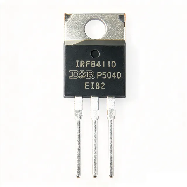

Spezifikationsvergleich
| Parameter | IRFB4110PBF | IRF1405PBF |
|---|---|---|
| Marke | Infineon | Infineon |
| Kategorie | MOSFETs | MOSFETs |
| Lebenszyklusstatus | Aktiv | Aktiv |
| Lagerstatus | In Stock | In Stock |
| Stückpreis (USD) | $1,55 | $1,42 |
| Transistortyp | N-Channel MOSFET | N-Channel MOSFET |
| Drain-Source Voltage (VDS) | 100 V | — |
| Continuous Drain Current (ID) at TC=25°C | 120 A (bond-wire limited) | — |
| Pulsed Drain Current (IDM) | [DATA_NEEDED: pulsed drain current] | — |
| Gate-Source Voltage (VGS) max | ±20 V | — |
| Gate Threshold Voltage (VGS(th)) | [DATA_NEEDED: VGS(th) typical/min/max] | — |
| On-Resistance RDS(on) max at VGS=10V | 4.5 mΩ | — |
| On-Resistance RDS(on) typ at VGS=10V | 3.7 mΩ | — |
| Power Dissipation (PD) at TC=25°C | 370 W | — |
| Betriebs-Sperrschichttemperatur | -55 °C to +175 °C | — |
| Gehäuse | TO-220AB (through-hole) | TO-220AB (through-hole) |
| Technology | HEXFET (planar DMOS) | HEXFET (Stripe Planar cell structure) |
| Montageart | Through Hole | Through Hole |
| RoHS-Status | Compliant (Pb-free suffix) | PbF suffix indicates lead-free / RoHS compliant |
| Lead-Free | Yes (PBF suffix denotes Pb-free) | — |
| Manufacturer | — | Infineon Technologies (formerly International Rectifier) |
| Part Number Suffix | — | PbF (lead-free, RoHS compliant) |
| Drain-Source Voltage (V_DS) | — | 55 V |
| Continuous Drain Current (I_D, Tc=25C) | — | 169 A |
| Continuous Drain Current (I_D, Tc=100C) | — | [DATA_NEEDED: I_D at Tc=100C] |
| Pulsed Drain Current (I_DM) | — | [DATA_NEEDED: pulsed drain current rating] |
| Maximum Power Dissipation (P_D, Tc=25C) | — | 330 W |
| R_DS(on) Maximum | — | 5.3 mOhm @ V_GS = 10 V |
| Gate Threshold Voltage (V_GS(th)) | — | 2.0 V to 4.0 V |
| Maximum Gate-Source Voltage (V_GS) | — | [DATA_NEEDED: maximum V_GS rating] |
| Operating Junction Temperature (T_J max) | — | 175 C |
| Storage Temperature Range | — | [DATA_NEEDED: storage temperature range] |
| Qualification | — | JEDEC qualified, optimized for switching below 100 kHz |
| Single Pulse Avalanche Energy (E_AS) | — | [DATA_NEEDED: avalanche energy rating] |
| Thermal Resistance Junction-to-Case (R_theta_JC) | — | [DATA_NEEDED: thermal resistance R_theta_JC] |