IRFB4110PBF vs IRF1405PBF Comparação
Comparação detalhada lado a lado de IRFB4110PBF por Infineon e IRF1405PBF por Infineon. Compare especificações principais, parâmetros elétricos, encapsulamento, status do ciclo de vida, preços e disponibilidade para determinar o melhor componente para os requisitos do seu projeto.
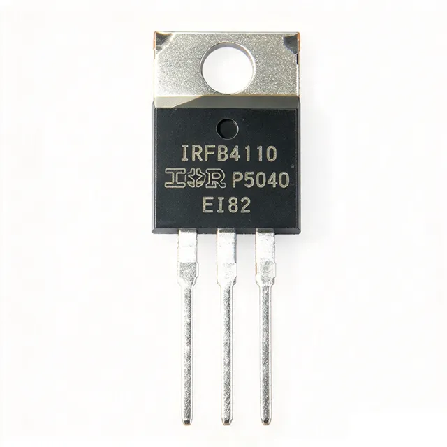

Comparação de especificações
| Parâmetro | IRFB4110PBF | IRF1405PBF |
|---|---|---|
| Marca | Infineon | Infineon |
| Categoria | MOSFETs | MOSFETs |
| Status do ciclo de vida | Ativo | Ativo |
| Status do estoque | In Stock | In Stock |
| Preço unitário (USD) | $1,55 | $1,42 |
| Tipo de transistor | N-Channel MOSFET | N-Channel MOSFET |
| Drain-Source Voltage (VDS) | 100 V | — |
| Continuous Drain Current (ID) at TC=25°C | 120 A (bond-wire limited) | — |
| Pulsed Drain Current (IDM) | [DATA_NEEDED: pulsed drain current] | — |
| Gate-Source Voltage (VGS) max | ±20 V | — |
| Gate Threshold Voltage (VGS(th)) | [DATA_NEEDED: VGS(th) typical/min/max] | — |
| On-Resistance RDS(on) max at VGS=10V | 4.5 mΩ | — |
| On-Resistance RDS(on) typ at VGS=10V | 3.7 mΩ | — |
| Power Dissipation (PD) at TC=25°C | 370 W | — |
| Temperatura de junção de operação | -55 °C to +175 °C | — |
| Encapsulamento | TO-220AB (through-hole) | TO-220AB (through-hole) |
| Technology | HEXFET (planar DMOS) | HEXFET (Stripe Planar cell structure) |
| Tipo de montagem | Through Hole | Through Hole |
| Status RoHS | Compliant (Pb-free suffix) | PbF suffix indicates lead-free / RoHS compliant |
| Lead-Free | Yes (PBF suffix denotes Pb-free) | — |
| Manufacturer | — | Infineon Technologies (formerly International Rectifier) |
| Part Number Suffix | — | PbF (lead-free, RoHS compliant) |
| Drain-Source Voltage (V_DS) | — | 55 V |
| Continuous Drain Current (I_D, Tc=25C) | — | 169 A |
| Continuous Drain Current (I_D, Tc=100C) | — | [DATA_NEEDED: I_D at Tc=100C] |
| Pulsed Drain Current (I_DM) | — | [DATA_NEEDED: pulsed drain current rating] |
| Maximum Power Dissipation (P_D, Tc=25C) | — | 330 W |
| R_DS(on) Maximum | — | 5.3 mOhm @ V_GS = 10 V |
| Gate Threshold Voltage (V_GS(th)) | — | 2.0 V to 4.0 V |
| Maximum Gate-Source Voltage (V_GS) | — | [DATA_NEEDED: maximum V_GS rating] |
| Operating Junction Temperature (T_J max) | — | 175 C |
| Storage Temperature Range | — | [DATA_NEEDED: storage temperature range] |
| Qualification | — | JEDEC qualified, optimized for switching below 100 kHz |
| Single Pulse Avalanche Energy (E_AS) | — | [DATA_NEEDED: avalanche energy rating] |
| Thermal Resistance Junction-to-Case (R_theta_JC) | — | [DATA_NEEDED: thermal resistance R_theta_JC] |