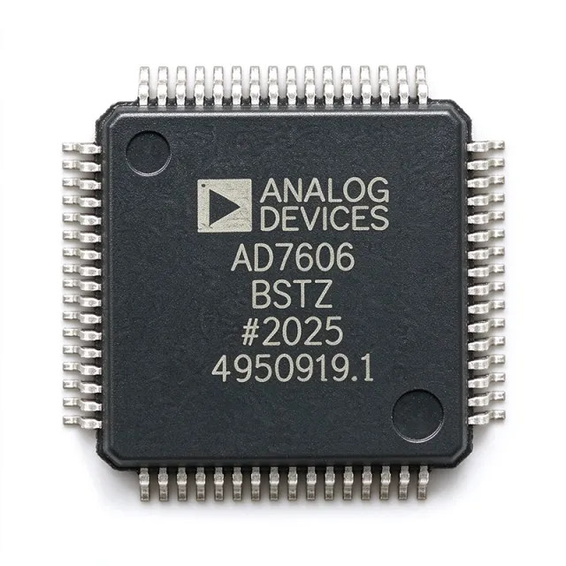
AD7606BSTZ - 16-Bit 8-Ch 200kSPS Simultaneous DAS ADC | Analog Devices
Teilenummer: AD7606BSTZ ✓ Aktiv| Menge | Stückpreis | Gesamt |
|---|---|---|
| 1 | $32.5 | $32,50 |
| 10 | $29.25 | $292,50 |
| 100 | $25.95 | $2.595,00 |
| 500 | $23.4 | $11.700,00 |
| 1.000 | $20.85 | $20.850,00 |
AD7606BSTZ Übersicht
A Data Acquisition System (DAS) is a complete mixed-signal front-end that conditions, samples, and digitizes multiple analog signals for a downstream host processor. The AD7606BSTZ sits in the family of simultaneous-sampling ADCs - between analog sensors and a DSP, FPGA, or microcontroller - and is a member of the broader converter hierarchy: ADC -> data converter -> mixed-signal IC -> semiconductor. Simultaneous-sampling DA conversion preserves the phase relationship between channels, a property that single-channel sequentially-sampling ADCs cannot deliver.
Key differentiating features include eight truly simultaneous track-and-hold channels, on-chip oversampling digital filter with 2x/4x/8x/16x/32x/64x ratios, integrated 2.5V reference with 10 ppm/°C drift, 1 MΩ analog input impedance that removes the need for external driver op-amps, and parallel/serial/SPI/QSPI/MICROWIRE-compatible digital I/O. Hardware-mode operation lets a host start conversions without writing any registers, useful for deterministic, low-latency control loops.
Technically, the ADC core is a charge-redistribution SAR converter followed by a flexible digital filter. The analog front end combines ±25V tolerant input clamps, a 1 MΩ input buffer, and a second-order Butterworth antialiasing filter with a -3 dB corner near 22 kHz at 200 kSPS. The integrated reference can be overdriven by an external low-impedance source when tighter accuracy is needed. Power consumption is approximately 215 mW when all eight channels sample at 200 kSPS from ±10V inputs.
Typical uses are three-phase power-line monitoring and protective relays (where phase-angle accuracy between voltage and current is critical), industrial motor control feedback, multi-axis vibration and modal analysis, and medical instrumentation. The bipolar ±10V/±5V ranges interface directly to current shunts and resistor-divider voltage networks, eliminating external signal conditioning. The eight-channel count suits four-quadrant power analyzers and multi-axis sensor pods without requiring an external mux.
When designing with this device, place 10 µF + 0.1 µF decoupling capacitors close to each AVCC pin and a single 10 µF + 0.1 µF pair on VDRIVE. Drive CONVSTA and CONVSTB simultaneously to guarantee true simultaneous sampling across all eight channels. If higher DC accuracy is required, drive REFIN/REFOUT from an external low-impedance reference rather than using the internal 2.5V source.
This page synthesizes distributor pricing, drop-in alternatives, and practical design notes not found in the manufacturer datasheet - useful for engineers qualifying second sources or planning migrations to the newer AD7606B family.
Drop-in-Alternativen für AD7606BSTZ – gleiches Gehäuse, Pin-kompatibel. Bauteile mit anderem Gehäuse, die eine PCB-Überarbeitung erfordern, sind ausgeschlossen.
Schnellvergleichstool – Wählen Sie Alternativbauteile für den Direktvergleich:
AD7606BSTZ-RL
✓ Auf Lager
$11.6 / Stück
Datenblatt ansehen →AD7606BSTZ-4
✓ Auf Lager
$11.6 / Stück
Datenblatt ansehen →AD7606BBCHIPS
✓ Auf Lager
$16.4 / Stück
Datenblatt ansehen →AD7606BBSTZ
📋 Referenzalternative (nicht im Katalog)
AD7606BSTZ Grenzwerte & elektrische Eigenschaften
| Part Number | AD7606BSTZ |
| Manufacturer | Analog Devices Inc. |
| Funktion | Data Acquisition System (DAS) with 16-bit SAR ADC |
| Number of Channels | 8 (simultaneous sampling) |
| Auflösung | 16 bit |
| Sampling Rate (per channel) | 200 kSPS |
| Throughput (aggregate) | 1.6 MSPS (8 channels × 200 kSPS) |
| Analog Input Range | ±10 V or ±5 V true bipolar (software/hardware selectable) |
| Analog Input Impedance | 1 MΩ (typ, with on-chip buffer) |
| Analog Supply Voltage (AVCC) | 4.75 V to 5.25 V (single 5 V supply) |
| Digital I/O Supply (VDRIVE) | 2.3 V to 5.25 V |
| On-chip Reference | 2.5 V, 10 ppm/°C drift (typ) |
| Antialiasing Filter | Second-order, -3 dB at ~22 kHz at 200 kSPS |
| Digital Filter | Programmable oversampling 2x/4x/8x/16x/32x/64x |
| Digital Interface | Parallel, serial, QSPI, MICROWIRE, SPI compatible |
| Input Overvoltage Protection | ±25 V analog input clamps |
| Betriebstemperatur | -40°C to +85°C (industrial) |
| Gehäuse | 64-lead LQFP (10 mm × 10 mm) |
| Montageart | Surface Mount |
| MSL-Level | 3 (per JEDEC J-STD-020) |
| RoHS-Status | Compliant |
AD7606BSTZ Pin-Konfiguration
| Pin 1 | V1 — Analog input channel 1 (true bipolar ±10V/±5V) |
| Pin 2 | V2 — Analog input channel 2 |
| Pin 3 | V3 — Analog input channel 3 |
| Pin 4 | V4 — Analog input channel 4 |
| Pin 5 | V5 — Analog input channel 5 |
| Pin 6 | V6 — Analog input channel 6 |
| Pin 7 | V7 — Analog input channel 7 |
| Pin 8 | V8 — Analog input channel 8 |
| Pin 9 | AGND — Analog ground |
| Pin 10 | REFIN/REFOUT — 2.5 V reference input/output (can be overdriven externally) |
| Pin 11 | REFCAP — Reference bypass capacitor pin |
| Pin 12 | REFGND — Reference ground |
| Pin 13 | AVCC — Analog 5 V supply |
| Pin 14 | AVCC — Analog 5 V supply |
| Pin 15 | AGND — Analog ground |
| Pin 16 | AGND — Analog ground |
| Pin 17 | RANGE — Analog input range select (0 = ±10V, 1 = ±5V) |
| Pin 18 | OS0 — Oversampling mode select bit 0 |
| Pin 19 | OS1 — Oversampling mode select bit 1 |
| Pin 20 | OS2 — Oversampling mode select bit 2 |
| Pin 21 | CONVST A — Conversion start input A (tie to CONVST B for simultaneous sampling) |
| Pin 22 | CONVST B — Conversion start input B |
| Pin 23 | BUSY — Output: indicates conversion in progress |
| Pin 24 | CS — Chip select (active low) |
| Pin 25 | RD — Read input (active low, parallel interface) |
| Pin 26 | RESET — Reset input (active high) |
| Pin 27 | STBY — Standby mode input |
| Pin 28 | DB0 — Parallel data output bit 0 (LSB when parallel mode) |
| Pin 29 | DB1 — Parallel data output bit 1 |
| Pin 30 | DB2 — Parallel data output bit 2 |
| Pin 31 | DB3 — Parallel data output bit 3 |
| Pin 32 | DB4 — Parallel data output bit 4 |
| Pin 33 | DB5 — Parallel data output bit 5 |
| Pin 34 | DB6 — Parallel data output bit 6 |
| Pin 35 | DB7 — Parallel data output bit 7 |
| Pin 36 | DB8 — Parallel data output bit 8 |
| Pin 37 | DB9 — Parallel data output bit 9 |
| Pin 38 | DB10 — Parallel data output bit 10 |
| Pin 39 | DB11 — Parallel data output bit 11 |
| Pin 40 | DB12 — Parallel data output bit 12 |
| Pin 41 | DB13 — Parallel data output bit 13 |
| Pin 42 | DB14 — Parallel data output bit 14 |
| Pin 43 | DB15/HBEN — Parallel data output bit 15 (MSB) / high-byte enable in serial mode |
| Pin 44 | DGND — Digital ground |
| Pin 45 | VDRIVE — Logic supply for digital I/O (2.3 V-5.25 V) |
| Pin 46 | DOUT A — Serial data output A (channels V1-V4) |
| Pin 47 | DOUT B — Serial data output B (channels V5-V8) |
| Pin 48 | DIN A — Serial data input A (daisy-chain) |
| Pin 49 | DIN B — Serial data input B (daisy-chain) |
| Pin 50 | SCLK A — Serial clock input A |
| Pin 51 | SCLK B — Serial clock input B |
| Pin 52 | FRSTDATA — First-data output flag in serial mode |
| Pin 53 | AVCC — Analog 5 V supply |
| Pin 54 | AVCC — Analog 5 V supply |
| Pin 55 | AGND — Analog ground |
| Pin 56 | AGND — Analog ground |
| Pin 57 | V1 — Analog input channel 1 redundant pin |
| Pin 58 | V2 — Analog input channel 2 redundant pin |
| Pin 59 | V3 — Analog input channel 3 redundant pin |
| Pin 60 | V4 — Analog input channel 4 redundant pin |
| Pin 61 | V5 — Analog input channel 5 redundant pin |
| Pin 62 | V6 — Analog input channel 6 redundant pin |
| Pin 63 | V7 — Analog input channel 7 redundant pin |
| Pin 64 | V8 — Analog input channel 8 redundant pin |
Typische Anwendungen
AD7606BSTZ ist geeignet für 6 Anwendungs: Three-Phase Power-Line Monitoring, Protective Relays, Industrial Motor Control, Multi-Axis Vibration and Modal Analysis, Medical Instrumentation and Patient Monitoring, Data Acquisition Systems and Instrumentation.
Three-Phase Power-Line Monitoring
The AD7606BSTZ is purpose-designed for three-phase power quality analyzers and smart meters. With 8 truly simultaneous-sampling 16-bit channels at 200 kSPS each, it captures three voltage channels, three current channels, and two auxiliary channels in a single acquisition window, preserving phase angle between voltage and current for accurate real/reactive/apparent power calculation. The ±10 V bipolar input range interfaces directly to PT secondary outputs (110 V/√3) through resistor dividers, and to CT secondary currents through burden resistors. According to the AD7606 datasheet, the 1 MΩ analog input impedance eliminates the need for external driver op-amps, simplifying BOM. The on-chip oversampling digital filter (2x-64x ratios) improves SNR by up to 11.6 dB, enabling class-0.2S revenue-meter accuracy from a single 5 V supply. Pair with an ARM Cortex-M4 host for IEC 61000-4-30 compliant power quality analysis.
Empfohlen
Protective Relays
In numerical protective relays for transmission and distribution, the AD7606BSTZ digitizes current and voltage waveforms at 16-bit resolution and 8 channels simultaneously, enabling fast fault detection within sub-cycle latency. The simultaneous sampling of all analog inputs at the rising edge of CONVST guarantees accurate phase-angle computation for differential protection, distance protection, and overcurrent detection. According to the Analog Devices AD7606 datasheet, the analog front end tolerates ±25 V transients, so external TVS protection is not required for normal fault conditions. The integrated oversampling digital filter lets you trade off bandwidth and noise rejection in real time, with no host CPU overhead. The 1 MΩ input impedance and on-chip analog input clamp protection reduce the relay's analog front-end complexity compared to discrete ADC-plus-op-amp designs. The industrial -40°C to +85°C operating range covers substation and switchgear environments.
Empfohlen
Industrial Motor Control
The AD7606BSTZ is a strong fit for closed-loop AC induction and permanent-magnet motor drives. It captures three phase currents, the DC bus voltage, and auxiliary signals simultaneously, eliminating the channel-to-channel skew that a multiplexed ADC would introduce. According to the Analog Devices AD7606 datasheet, the 200 kSPS per channel throughput exceeds typical 5 kHz current-loop bandwidth needs by more than 10x, allowing precise space-vector PWM synchronization and field-oriented control. The ±10 V input range accepts current-sense amplifier outputs (e.g., AD8205, AD8210) directly, and the 1 MΩ input impedance minimizes loading of the sense circuit. The 16-bit resolution delivers ENOB ≥14 bits at lower oversampling ratios, supporting smooth low-RPM torque control. Hardware-mode CONVST operation keeps the digital interface deterministic for real-time control loops without firmware overhead.
Empfohlen
Multi-Axis Vibration and Modal Analysis
For modal analysis, structural testing, and condition-based monitoring of rotating machinery, the AD7606BSTZ digitizes 8 accelerometer or IEPE sensor channels simultaneously, which is essential to capture the true relative phase between vibration points on a structure. Without simultaneous sampling, modal-shape calculations become meaningless because the time skew between channels corrupts transfer-function estimates. According to the AD7606 datasheet, the 200 kSPS per channel throughput supports vibration bandwidth up to ~80 kHz with the integrated oversampling filter active. The 16-bit resolution delivers >85 dB dynamic range, sufficient to resolve low-level harmonics against the fundamental vibration tone. The integrated antialiasing filter (-3 dB at 22 kHz at 200 kSPS) prevents aliasing of out-of-band mechanical noise without external RC stages. ±5 V input range suits IEPE constant-current powered accelerometers via standard 4 mA bias networks.
Empfohlen
Medical Instrumentation and Patient Monitoring
The AD7606BSTZ is well-suited to multi-channel patient-monitoring front ends such as ECG, EEG, EMG, and multi-lead cardiac monitors. According to the Analog Devices AD7606 datasheet, the simultaneous sampling of 8 leads preserves inter-lead phase relationships needed for accurate 12-lead ECG reconstruction, while the 16-bit resolution and integrated digital oversampling filter deliver the noise-floor performance required for diagnostic-grade cardiology. The 1 MΩ input impedance matches clinical-electrode isolation amplifiers without loading distortion. The bipolar ±5 V input range accommodates standard 1 V/mV electrode signals after instrumentation-amp scaling. The hardware CONVST mode supports deterministic sampling intervals without firmware variability - critical for heart-rate-variability measurement. The single 5 V supply simplifies IEC 60601-1 isolation design and reduces the battery-management burden on portable monitors.
Empfohlen
Data Acquisition Systems and Instrumentation
For general-purpose bench-top and rack-mount data loggers, the AD7606BSTZ provides 8 simultaneous high-resolution channels with parallel/serial interface flexibility. According to the Analog Devices AD7606 datasheet, the 200 kSPS per channel aggregate 1.6 MSPS throughput and integrated oversampling filter support transducer applications such as strain gauges, pressure sensors, and thermocouple arrays. The single 5 V analog supply and separate VDRIVE (2.3 V-5 V) host interface simplify integration with legacy 5 V PLCs and modern 3.3 V FPGAs without level shifters. The integrated 2.5 V reference (10 ppm/°C) eliminates external reference components, reducing BOM cost for multi-channel loggers. Hardware-mode operation lets a PLC or FPGA start conversions without firmware, ideal for deterministic control and test systems. The industrial -40°C to +85°C temperature range covers laboratory, factory-floor, and outdoor instrumentation use cases.
Empfohlen
Zusammenfassung der empfohlenen Produkte
Technische Referenzdaten für AD7606BSTZ – Vergleich, Designhinweise und Compliance-Informationen.
Auswahlhilfe
Vergleich mit Alternativen
| Parameter | Dieses Produkt | AD7606BSTZ-RL | AD7606BSTZ-4 | AD7606BBSTZ |
|---|---|---|---|---|
| Package | 64-LQFP (10x10 mm) | 64-LQFP (10x10 mm) - same | 64-LQFP (10x10 mm) - same | 64-LQFP (10x10 mm) - same |
| Brand | Analog Devices | Analog Devices | Analog Devices | Analog Devices |
| Resolution | 16 bit | 16 bit | 16 bit | 16 bit |
| Channels (simultaneous) | 8 | 8 | 4 | 8 |
| Throughput per Channel | 200 kSPS | 200 kSPS | 200 kSPS | 800 kSPS (+300%) |
| Analog Input Range | ±10 V / ±5 V bipolar | ±10 V / ±5 V bipolar | ±10 V / ±5 V bipolar | ±10 V / ±5 V bipolar |
| On-chip Reference | 2.5 V, 10 ppm/°C | 2.5 V, 10 ppm/°C | 2.5 V, 10 ppm/°C | 2.5 V, 5 ppm/°C |
| Oversampling Filter Ratios | 2x, 4x, 8x, 16x, 32x, 64x | 2x-64x | 2x-64x | 2x-256x |
| Operating Temperature | -40°C to +85°C | -40°C to +85°C | -40°C to +85°C | -40°C to +125°C |
| Approx. Unit Price @ 1ku (USD) | ~$25.50 | ~$25.50 | ~$24.00 | ~$30.00 |
Wichtigste Unterscheidungsmerkmale
- Eight true simultaneous-sampling channels with on-chip track-and-hold (vs. AD7606BSTZ-4)
- Newer generation 800 kSPS throughput and wider temperature range (vs. AD7606BBSTZ)
- 16-bit resolution preserves more than 14-bit ENOB (vs. AD7607BSTZ (14-bit))
- Integrated 2.5V reference with 10 ppm/°C drift (vs. External reference design with ADR01)
Designhinweise
Decouple each AVCC pin (4 pins on the LQFP) with a 10 µF tantalum or ceramic plus a 0.1 µF ceramic placed within 5 mm of the pin. Place a single 10 µF + 0.1 µF pair on VDRIVE. The REFCAP pin requires a 10 µF ceramic to AGND with <2 mΩ ESR for low reference noise. Estimated: with all 8 channels active at 200 kSPS and ±10V inputs, AVCC current draw reaches ~215 mW total - the 0.1 µF cap handles high-frequency transients from SAR switching while the 10 µF handles low-frequency ripple. Reference: ADI AD7606 datasheet, power-supply-decoupling section.
Route analog input traces V1-V8 as matched-length differential pairs with continuous ground shielding, keeping them away from digital lines (DB0-DB15, SCLK, CONVST). Use a split ground plane with AGND and DGND tied at a single point near the AVCC decoupling cap, and place the AD7606BSTZ so that the AGND pin side faces the analog input connectors. The exposed thermal pad on the LQFP must be soldered to a copper area for mechanical stability, even though the device does not require heatsinking. Reference: ADI AD7606 datasheet, layout guidelines.
Tie CONVST A and CONVST B together and drive them with a single low-skew logic signal - otherwise channels A-D and channels E-H will not sample at the same instant and your phase-angle calculations will be corrupted. Do not leave any analog input pin floating; unused channels must be tied to mid-supply (0 V) through a 1 kΩ value-level reference network to prevent the ±25 V clamps from conducting continuously. The RESET pin should be tied to DGND through a 10 kΩ pull-down with a 100 nF cap to AGND for power-on-reset, unless the host provides an active reset signal. Reference: ADI AD7606 datasheet, reset section.
Estimated: the SAR ADC input presents transient current spikes on each conversion edge; place the 10 µF + 0.1 µF AVCC decoupling within 5 mm to keep these transients off the supply rail. Avoid using the internal reference to drive external loads - if the application requires a buffered reference elsewhere, use an external ADR421 or ADR4525 and overdrive REFIN/REFOUT through 10 kΩ. For the highest DC accuracy, drive OS0/OS1/OS2 to select an oversampling ratio of at least 4x, which improves SNR by ~3 dB and reduces broadband noise by ~½. Reference: ADI AD7606 datasheet, noise performance section.
Estimated: at VIN=5V, VDRIVE=3.3V, and 200 kSPS throughput on all 8 channels, the AD7606BSTZ dissipates approximately 215 mW into the 64-LQFP package (theta_JA ~50 °C/W on a 4-layer JEDEC test PCB). Junction temperature rise above ambient is ~11 °C, which is well within the 125 °C absolute maximum, so no heatsink is required for normal industrial operation. If you must sample all 8 at 200 kSPS continuously in a sealed chassis, ensure at least 1 cm² of exposed pad-top copper to keep junction rise under 10 °C. Reference: ADI AD7606 datasheet, thermal resistance section.
Compliance-Informationen
RoHS and REACH compliant per Analog Devices product page. Lead-free finish (NiPdAu). Not AEC-Q100 qualified - designed for industrial (-40°C to +85°C) applications. Halogen-free status: not explicitly stated in verified data. Conflict-minerals compliant per ADI corporate policy.







