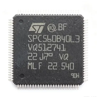
GD32F105VCT6 - 108MHz Cortex-M3 MCU 256KB Flash LQFP-100
Teilenummer: GD32F105VCT6 ✓ Aktiv| Menge | Stückpreis | Gesamt |
|---|---|---|
| 1 | $2.45 | $2,45 |
| 10 | $2.21 | $22,10 |
| 100 | $1.95 | $195,00 |
| 500 | $1.72 | $860,00 |
| 1.000 | $1.55 | $1.550,00 |
GD32F105VCT6 Übersicht
A microcontroller (MCU) is an integrated circuit that combines a CPU core, program memory, working memory, and I/O peripherals on a single silicon die. Within the semiconductor taxonomy, the GD32F105VCT6 sits at the hierarchy Microcontroller -> 32-bit MCU -> ARM Cortex-M3 MCU -> mainstream MCU -> GigaDevice GD32 family. It is designed as a drop-in upgrade path for STM32F103-class designs while adding USB OTG that STM32F103 lacks.
Key features include 108 MHz max CPU clock with single-cycle multiply and hardware divide, a 12-bit ADC with up to 16 channels and 1 MSPS conversion rate, two 12-bit DAC channels, three general-purpose 16-bit timers plus one PWM timer, two USARTs plus two UARTs, two SPIs, two I2Cs, one USB FS OTG, one CAN 2.0B, and an operating voltage range of 2.6V to 3.6V. The device also supports external interrupts on all GPIO pins and a 7-channel DMA controller.
The GD32F105VCT6 uses a 3-stage pipelined Cortex-M3 core with Thumb-2 instruction set, delivering 1.25 DMIPS/MHz (90 DMIPS at 72 MHz equivalent). Flash controller prefetch and 64-bit-wide Flash access deliver up to 50% higher CoreMark scores than competing Cortex-M3 parts at the same clock, making it well suited to real-time control loops, USB peripherals, and motor-control firmware.
Typical applications include USB HID/CDC peripherals, industrial control boards, smart home gateways, motor drive controllers, consumer appliances, and cost-optimized IoT nodes. The LQFP-100 footprint matches the STM32F105/F103 100-pin layout, enabling reuse of existing PCB designs.
When designing with this device, ensure the external 8 MHz HSE crystal is selected to drive the 108 MHz PLL; for USB applications a 48 MHz clock-accurate source is required. Decouple VDD/VDDA pins with 100 nF ceramics close to each pin and provide a 4.7 uF bulk capacitor for ADC noise suppression.
This page synthesizes distributor pricing from LCSC and Pacific Component Xchange, drop-in alternatives from the STM32F103/F105 family, and practical design notes not consolidated in any single manufacturer document.
Drop-in-Alternativen für GD32F105VCT6 – gleiches Gehäuse, Pin-kompatibel. Bauteile mit anderem Gehäuse, die eine PCB-Überarbeitung erfordern, sind ausgeschlossen.
Varianten dieser Serie
Modelle derselben Serie, die drop-in-kompatibel sind mit GD32F105VCT6 (gleiche Bauform und Footprint) – abweichend in ADC, CAN, DAC, I2C, Operating Temperature.
Schnellvergleichstool – Wählen Sie Alternativbauteile für den Direktvergleich:
GD32F105VCT6
✅ Drop-In ⚠️ Spezifikationen ungeprüft✓ Auf Lager
$1.55 / Stück
Datenblatt ansehen →GD32F105VDT6
✅ Drop-In ⚠️ Spezifikationen ungeprüft📋 Referenzalternative (nicht im Katalog)
STM32F105VCT6
✅ Drop-In✓ Auf Lager
$5.4 / Stück
STM32F103VCT6
✅ Drop-In✓ Auf Lager
$2.68 / Stück
Datenblatt ansehen →GD32F103VCT6
✅ Drop-In ⚠️ Spezifikationen ungeprüft📋 Referenzalternative (nicht im Katalog)
GD32F105VCT6 Grenzwerte & elektrische Eigenschaften
| Core | ARM Cortex-M3 32-bit |
| Maximum CPU Clock | 108 MHz |
| Flash Memory | 256 KB |
| SRAM | 64 KB |
| Operating Voltage | 2.6 V to 3.6 V |
| ADC | 2 x 12-bit, 1 MSPS, up to 16 channels |
| DAC | 2 x 12-bit |
| USB | USB 2.0 Full-Speed OTG |
| CAN | 1 x CAN 2.0B |
| UART/USART | 2 x USART + 2 x UART |
| SPI | 2 x SPI |
| I2C | 2 x I2C |
| Timers | 3 x 16-bit GP + 1 x PWM |
| DMA Channels | 7 |
| Gehäuse | LQFP-100 (14x14 mm) |
| Betriebstemperatur | -40 C to +85 C (industrial) |
| Montageart | Surface Mount |
| RoHS-Status | Compliant |
GD32F105VCT6 lqfp-100 (14x14 mm) Pinbelegungsleitfaden
Pinbelegung für GD32F105VCT6 (lqfp-100 (14x14 mm)-Gehäuse). Dieser digitale IC umfasst GPIO, Kommunikationsschnittstellen (UART, SPI, I2C) und Versorgungspins. Alternative Pin-Funktionen und Konfigurationsoptionen entnehmen Sie dem Herstellerdatenblatt. Unverzichtbar für Embedded-System-Design und PCB-Layout.
Keine detaillierten Pinbelegungsdaten verfügbar für GD32F105VCT6.
Siehe die Datenblatt für die vollständige Pin-Konfiguration.
Typische Anwendungen
GD32F105VCT6 ist geeignet für 7 Anwendungs: USB HID / CDC Peripherals, Industrial Control Boards, Motor Drive Controllers, Smart Home Gateways, Consumer Appliance Controllers, Cost-Optimized IoT Nodes, HMI Touch Panels.
USB HID / CDC Peripherals
The GD32F105VCT6's integrated USB 2.0 Full-Speed OTG controller with on-chip PHY makes it ideal for USB HID keyboards, mice, game controllers, and CDC virtual COM port devices without needing an external PHY chip. Its 108 MHz Cortex-M3 core handles USB interrupt latency with comfortable headroom while servicing HID reports and LED scan routines simultaneously. The 64 KB SRAM accommodates USB HID report buffers plus application stacks; the 256 KB Flash is sufficient for composite USB device firmware, bootloader, and OTA update partitions. Connect DP/DM lines directly to the USB connector with the required 33 ohm series resistors and ESD protection. For full-speed USB certification, follow the USB 2.0 reference clock accuracy requirement of 2500 ppm at the 48 MHz USB clock derived from the PLL.
Empfohlen
Industrial Control Boards
The GD32F105VCT6 suits industrial control applications including PLC expansion modules, sensor aggregation nodes, and HMI panels that need CAN 2.0B for fieldbus communication, two 12-bit ADCs for analog signal acquisition, and a robust 108 MHz Cortex-M3 core for deterministic control loops. Its -40 C to +85 C industrial temperature range and 2.6V to 3.6V supply tolerance handle 24V industrial rails regulated down to 3.3V. The 16 ADC channels support multi-sensor monitoring (temperature, pressure, current), while the CAN peripheral interfaces with industrial fieldbus networks. The LQFP-100 footprint is well suited to 4-layer industrial PCBs with creepage/clearance requirements.
Empfohlen
Motor Drive Controllers
The GD32F105VCT6's 108 MHz Cortex-M3 core delivers the computational throughput needed for FOC (field-oriented control) of BLDC and PMSM motors up to several kilowatts. The advanced PWM timer supports complementary 3-phase outputs with programmable dead-time insertion and hardware break inputs for overcurrent protection. With 16 ADC channels sampled at 1 MSPS, simultaneous current and voltage sensing is achievable, while the 256 KB Flash stores complex motor control algorithms including sensorless observers. The CAN peripheral interfaces with industrial servo networks; the 64 KB SRAM accommodates control loop buffers and parameter tables. Use the LQFP-100 footprint for adequate thermal dissipation at 108 MHz operation.
Empfohlen
Smart Home Gateways
The GD32F105VCT6 is well matched to smart home gateway hubs that aggregate Zigbee, Wi-Fi, and Bluetooth data via UART or SPI bridges. Its 108 MHz CPU processes encrypted MQTT messages, the 64 KB SRAM handles TLS buffers, and the 256 KB Flash stores gateway firmware plus a secondary OTA bootloader. The two 12-bit DACs are useful for audio feedback in voice-control hubs. The integrated USB OTG allows the gateway to expose a configuration CDC port to a host PC for first-time setup. The 2.6V to 3.6V supply range matches typical 3.3V regulated rails from USB or wall adapters. For multi-radio gateways, add an external Wi-Fi/BT module via SPI or SDIO.
Empfohlen
Consumer Appliance Controllers
Consumer appliances including washing machines, air conditioners, and induction cookers benefit from the GD32F105VCT6's combination of 108 MHz performance, CAN bus for inverter communication, 16 ADC channels for temperature and current sensing, and integrated USB for service diagnostics. The Cortex-M3 core runs PID control loops and user-interface firmware simultaneously; the 256 KB Flash supports multi-language firmware and graphical UI assets. The two 12-bit DACs drive audio cues for end-of-cycle alerts. Operating temperature range of -40 C to +85 C handles the thermal environment inside appliance enclosures. The LQFP-100 package is easy to hand-solder for prototype runs.
Empfohlen
Cost-Optimized IoT Nodes
The GD32F105VCT6's LCSC pricing of $2.45 at qty 1 (and dropping to roughly $1.55 at qty 1000) makes it attractive for low-cost IoT sensor nodes that need more compute than Cortex-M0+ parts but cannot justify Cortex-M4 pricing. The 108 MHz core runs light-weight TLS, CoAP, or LoRaWAN stacks; the 64 KB SRAM holds network buffers and sensor fusion data; the 256 KB Flash supports OTA-capable firmware with two partitions. The two USART interfaces connect to LoRa or NB-IoT modems; the I2C buses interface with environmental sensors and EEPROMs. For battery-powered deployments, the device supports low-power Run, Sleep, and Stop modes.
Empfohlen
HMI Touch Panels
The GD32F105VCT6 drives small to mid-size HMI panels with TFT LCDs up to 4.3 inches when paired with an external display controller via SPI or FSMC. Its 108 MHz core renders button widgets and updates screens at 30+ fps; the 64 KB SRAM stores frame buffers or partial screens; the 256 KB Flash holds UI assets, fonts, and multi-language strings. The two 12-bit DACs drive backlight brightness with hardware PWM-free control; the timers generate LCD timing signals. The USB OTG port accepts firmware updates from a USB stick in field service scenarios. Industrial temperature range supports outdoor and automotive cabin installations.
Empfohlen
Zusammenfassung der empfohlenen Produkte
Technische Referenzdaten für GD32F105VCT6 – Vergleich, Designhinweise und Compliance-Informationen.
Auswahlhilfe
Vergleich mit Alternativen
| Parameter | Dieses Produkt | GD32F105VCT6 | GD32F105VDT6 | STM32F105VCT6 | STM32F103VCT6 | GD32F103VCT6 |
|---|---|---|---|---|---|---|
| Brand | GigaDevice | GigaDevice | GigaDevice | STMicroelectronics | STMicroelectronics | GigaDevice |
| Package | LQFP-100 | LQFP-100 - same | LQFP-100 - same | LQFP-100 - same | LQFP-100 - same | LQFP-100 - same |
| Core | ARM Cortex-M3 | Cortex-M3 | Cortex-M3 | Cortex-M3 | Cortex-M3 | Cortex-M3 |
| Maximum CPU Clock | 108 MHz | 108 MHz | 108 MHz | 72 MHz | 72 MHz | 108 MHz |
| Flash Memory | 256 KB | 256 KB | 256 KB | 256 KB | 256 KB | 256 KB |
| SRAM | 64 KB | 64 KB | 64 KB | 64 KB | 64 KB | 64 KB |
| USB | USB FS OTG | USB FS OTG | USB FS OTG | USB FS OTG | USB FS Device only | USB FS Device only |
| CAN | 1 x CAN 2.0B | 1 x CAN 2.0B | 1 x CAN 2.0B | 1 x CAN 2.0B | 1 x CAN 2.0B | 1 x CAN 2.0B |
| ADC | 2 x 12-bit 1 MSPS | 2 x 12-bit 1 MSPS | 2 x 12-bit 1 MSPS | 2 x 12-bit 1 MSPS | 2 x 12-bit 1 MSPS | 2 x 12-bit 1 MSPS |
| Operating Voltage | 2.6 V to 3.6 V | 2.6 V to 3.6 V | 2.6 V to 3.6 V | 2.0 V to 3.6 V | 2.0 V to 3.6 V | 2.6 V to 3.6 V |
Wichtigste Unterscheidungsmerkmale
- Higher CPU clock than cross-brand STM32 equivalent (vs. STM32F105VCT6)
- USB OTG included versus STM32F103 USB Device-only (vs. STM32F103VCT6)
- Same-brand family variant for upgrade path (vs. GD32F105VDT6)
Designhinweise
Decouple every VDD pin with a 100 nF X7R ceramic placed within 3 mm of the pin, and add a shared 4.7 uF X5R bulk capacitor near the voltage regulator. The VDDA pin should have its own 100 nF + 1 uF filter network to keep ADC noise low. For USB applications, ensure VDD does not drop below 3.0V during USB enumeration peaks - a 100 uF bulk cap at the USB connector is recommended.
The GD32F105VCT6 PLL requires an 8 MHz external HSE crystal (or oscillator) to generate the 108 MHz system clock. According to the GigaDevice GD32F105xx datasheet, the PLL configuration register differs from STM32F103, so always use the GigaDevice firmware library or reference manual when setting up the clock tree. For USB FS operation, the 48 MHz USB clock must be within 2500 ppm accuracy, requiring a crystal with low load capacitance drift.
Use a 4-layer PCB with a dedicated ground plane and a 3.3V power plane. Keep the HSE crystal traces short (under 5 mm) and surround them with a ground guard ring to reduce EMI. The LQFP-100 package requires thermal vias under the exposed pad (if present) for adequate heat dissipation at 108 MHz operation. Route USB DP/DM as a 90 ohm differential pair with length matching within 2 mm.
Do not assume GD32 registers match STM32F103 bit-for-bit; the USB OTG peripheral and EXTI trigger selection registers differ. Always use the GigaDevice standard peripheral library or HAL. The BOOT0 pin must be pulled low for normal boot from Flash; leaving it floating causes boot from system memory bootloader, which can confuse factory programming. The LQFP-100 has two VSS pins that must both be connected to ground for proper operation.
Estimated: At 108 MHz with all peripherals active, the GD32F105VCT6 consumes approximately 50 mA from VDD (3.3V), giving 165 mW power dissipation. With LQFP-100 theta_JA around 50 C/W on a standard 4-layer JEDEC test board, junction temperature rise is about 8 C above ambient. The industrial -40 C to +85 C operating range provides adequate margin for enclosed designs without forced cooling.
Compliance-Informationen
RoHS compliance per LCSC and GigaDevice product page. AEC-Q100 automotive qualification not confirmed in the verified data; this part targets industrial and consumer markets. Halogen-free status and conflict minerals declaration not provided in the verified web data.