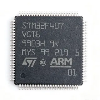
STM32F103VCT6 - 256KB Flash Cortex-M3 MCU 72MHz | ST
MPN: STM32F103VCT6 ✓ Active| Qty | Unit Price | Extended |
|---|---|---|
| 1 | $3.85 | $3.85 |
| 10 | $3.47 | $34.70 |
| 100 | $3.12 | $312.00 |
| 500 | $2.95 | $1,475.00 |
| 1,000 | $2.68 | $2,680.00 |
STM32F103VCT6 Overview
What is a microcontroller? A microcontroller (MCU) is a single-chip computer that integrates a processor core, memory, and programmable peripherals to govern a specific embedded operation. The STM32F103 series sits within the broader hierarchy of 32-bit Flash MCUs based on the Arm Cortex-M processor family and is one of the most widely deployed general-purpose MCU lines in industrial control, consumer electronics, and IoT devices.
Key features include three 12-bit ADCs with up to 21 channels, two 12-bit DACs, and a rich communication set: three USARTs, two I2C, three SPI, one USB 2.0 full-speed device, one CAN 2.0B, and one SDIO interface. Advanced timers support PWM generation and motor control, while a 12-channel DMA controller offloads data movement from the CPU.
The Cortex-M3 core executes the Thumb-2 instruction set with a hardware divide unit, delivering strong code density and deterministic interrupt handling through the nested vectored interrupt controller (NVIC). Debugging is supported via both JTAG and serial wire debug (SWD). The device operates from a 2.0 V to 3.6 V supply over an industrial -40C to +85C temperature range, with a real-time clock and low-power sleep, stop, and standby modes for battery-sensitive designs.
Typical applications include motor control (advanced timers generate PWM while ADCs sample current feedback), industrial automation PLCs, and USB/CAN communication nodes in metering and gateways.
Design consideration: configure BOOT0 correctly for the boot source and decouple every VDD/VSS pair with 100 nF capacitors; connect VDDA to a clean filtered analog supply for full ADC accuracy.
This page adds value beyond the datasheet with verified drop-in alternatives, distributor pricing, and practical design notes.
Drop-in alternatives for STM32F103VCT6 — same package, pin-to-pin compatible. Different-package parts requiring PCB rework are excluded.
Variants in this series
Same-series models that are drop-in compatible with STM32F103VCT6 (same form factor and footprint) — differing in Timers, Core, Operating Temperature, ADC, Package.
Quick Comparison Tool — Select alternative parts for side-by-side comparison:
STM32F103VET6
✅ Drop-In✓ In Stock
$3.85 / Unit
View Datasheet →STM32F103VDT6
✅ Drop-In✓ In Stock
$7.1591 / Unit
View Datasheet →STM32F103VBT6
✅ Drop-In✓ In Stock
$3.33 / Unit
View Datasheet →GD32F103VCT6
✅ Drop-In📋 Reference alternative (not in catalog)
APM32F103VCT6
✅ Drop-In📋 Reference alternative (not in catalog)
STM32F103VCT6 Maximum Ratings & Electrical Characteristics
| Core | ARM Cortex-M3 |
| Maximum CPU Frequency | 72 MHz |
| Flash Memory | 256 KB |
| SRAM | 48 KB |
| Supply Voltage Range | 2.0 V to 3.6 V |
| Operating Temperature | -40C to +85C |
| Package | LQFP-100 (14x14 mm) |
| I/Os | 80 |
| ADC | 3x 12-bit, up to 21 channels |
| DAC | 2x 12-bit |
| USART | 3 |
| SPI | 3 |
| I2C | 2 |
| USB | USB 2.0 full-speed device |
| CAN | 1x CAN 2.0B |
| SDIO | 1 |
| Timers | Advanced, general-purpose and basic timers (PWM capable) |
| DMA Channels | 12 |
| Debug Interfaces | JTAG, SWD |
| Mounting Type | Surface Mount |
STM32F103VCT6 lqfp-100 (14x14 mm) Pin Configuration Guide
Pin configuration for STM32F103VCT6 (lqfp-100 (14x14 mm) package). This digital IC includes GPIO, communication interfaces (UART, SPI, I2C), and power pins. Refer to the manufacturer datasheet for alternate pin functions and configuration options. Essential for embedded system design and PCB layout.

No detailed pinout data available for STM32F103VCT6.
Refer to the datasheet for full pin configuration.
Typical Applications
STM32F103VCT6 is suitable for 6 applications: Motor Control (BLDC/PMSM Inverters), Industrial Automation and PLC I/O, USB Devices and Gateways, IoT Sensor Nodes and Gateways, Medical and Diagnostic Instruments, Consumer Electronics and HMI Panels.
Motor Control (BLDC/PMSM Inverters)
The STM32F103VCT6 fits motor control because its advanced timers produce complementary PWM outputs with hardware dead-time insertion while the three 12-bit ADCs synchronize to the PWM carrier to sample phase currents at the center of the pulse, minimizing switching-noise error. ST's STM32 MC SDK supports FOC firmware directly on the F1 high-density line, using the 72 MHz Cortex-M3 for field-oriented control loops at 10-20 kHz. In a typical three-phase inverter, the MCU interfaces with a gate driver over GPIO and reads bus voltage through the ADC; DMA channels stream current samples without CPU load. The trade-off versus a dedicated motor MCU is the absence of an FPU, so fixed-point arithmetic is used.
Recommended
Industrial Automation and PLC I/O
The STM32F103VCT6 suits industrial automation nodes because it combines CAN 2.0B for fieldbus communication, three USARTs for Modbus RTU links, and 80 GPIOs in one LQFP-100 device - enough to handle digital I/O banks, relay drivers, and analog conditioning from the 12-bit ADCs. Its -40C to +85C industrial temperature grade and 2.0-3.6 V operation tolerate factory-floor supply variation, while the independent watchdog and brown-out reset improve uptime. The CAN interface connects the node to higher-level controllers without an external transceiver controller. Firmware typically fits comfortably in the 256 KB Flash, leaving room for OTA-style field updates via the UART bootloader.
Recommended
USB Devices and Gateways
The integrated USB 2.0 full-speed device controller makes the STM32F103VCT6 a classic choice for USB virtual-COM-port devices, HID instruments, and custom class devices - no external USB chip is needed. Combined with the SDIO host interface, it also serves as a data logger that streams sensor data to removable storage and uploads over USB. The 72 MHz core sustains the 12 Mbit/s full-speed bandwidth with DMA support, and ST provides a mature USB device library with CDC/HID/MSC classes. Designers must add a 1.5 kOhm pull-up on D+ (or use the internal pull-up where supported) and respect crystal accuracy requirements for USB clock tolerance.
Recommended
IoT Sensor Nodes and Gateways
For IoT nodes, the STM32F103VCT6 balances performance and power: sleep, stop, and standby modes reduce current draw, the RTC maintains timekeeping in low-power states, and the 256 KB Flash accommodates a TCP/IP or LoRaWAN stack alongside application logic. Communication to radio modules typically uses SPI (3 available) or USART (3 available), and the 12-bit ADCs read battery voltage and analog sensors directly. The wide 2.0-3.6 V supply range allows direct operation from a lithium cell through an LDO. The trade-off versus newer STM32L-series parts is higher active current, so battery designs with strict budgets should compare against STM32L4 options.
Recommended
Medical and Diagnostic Instruments
Benchtop medical devices such as blood-pressure monitors, glucose analyzers, and portable diagnostic tools use the STM32F103VCT6 for its three 12-bit ADCs with up to 21 channels, which sample sensor front-ends, and its USART/USB interfaces for data export. The 72 MHz Cortex-M3 runs filtering and measurement algorithms deterministically thanks to the NVIC's low interrupt latency, and 48 KB SRAM buffers acquisition windows. Separate VDDA/VREF+ pins allow a clean analog supply rail, critical for measurement accuracy. Note that the commercial temperature grade and non-medical qualification mean system-level validation is required for any patient-connected design, often alongside an isolation barrier.
Recommended
Consumer Electronics and HMI Panels
The STM32F103VCT6 is a proven HMI controller for appliance panels, thermostats, and access-control terminals: 80 GPIOs drive keypads, LEDs, and relays, while the FSMC flexible static memory controller interfaces TFT LCD modules over a parallel bus, and SPI drives touch controllers. The 256 KB Flash stores graphics assets and a GUI framework, and the two 12-bit DACs can generate audio alerts. The mature Arduino-style ecosystem and low board cost make it a staple of consumer product development. For richer graphics, designers upgrade to STM32F4-class parts with Chrom-ART acceleration, accepting higher cost and a different package.
Recommended
Recommended Products Summary
Engineering reference data for STM32F103VCT6 — comparison, design guidance, and compliance information.
Selection Guide
Comparison with Alternatives
| Parameter | This Product | STM32F103VET6 | STM32F103VDT6 | STM32F103VBT6 | GD32F103VCT6 | APM32F103VCT6 |
|---|---|---|---|---|---|---|
| Package | LQFP-100 (14x14 mm) | LQFP-100 - same | LQFP-100 - same | LQFP-100 - same | LQFP-100 - same | LQFP-100 - same |
| Brand | STMicroelectronics | STMicroelectronics | STMicroelectronics | STMicroelectronics | GigaDevice | Geehy |
| Core / Max Frequency | Cortex-M3 @ 72 MHz | Cortex-M3 @ 72 MHz | Cortex-M3 @ 72 MHz | Cortex-M3 @ 72 MHz | Cortex-M3 @ 108 MHz | Cortex-M3 @ 72 MHz |
| Flash Memory | 256 KB | 512 KB | 384 KB | 128 KB | 256 KB | 256 KB |
| SRAM | 48 KB | 64 KB | 64 KB | 16 KB | 48 KB | 48 KB |
| ADC / DAC | 3x 12-bit ADC, 2x 12-bit DAC | 3x 12-bit ADC, 2x 12-bit DAC | 3x 12-bit ADC, 2x 12-bit DAC | 2x 12-bit ADC, 2x DAC | 3x 12-bit ADC, 2x DAC | 3x 12-bit ADC, 2x DAC |
| USB / CAN | USB 2.0 FS device + CAN 2.0B | USB FS + CAN 2.0B | USB FS + CAN 2.0B | USB FS + CAN 2.0B | USB FS + CAN 2.0B | USB FS + CAN 2.0B |
| Software Compatibility | STM32F1 reference (HAL/StdPeriph, CubeMX) | 100% - same family | 100% - same family | 100% - same family | Register-compatible, minor flash/USB timing differences | Largely compatible, verify peripheral timing |
Key Differentiators
- Largest mainstream ecosystem at lowest risk (vs GD32F103VCT6)
- Balanced memory for mid-size firmware (vs STM32F103VBT6)
- Cost-optimized versus higher-density siblings (vs STM32F103VET6)
Design Notes
Decouple every VDD/VSS pair with 100 nF ceramic capacitors placed within 5 mm of the pins, plus one bulk 4.7-10 uF capacitor near the device. Connect VDDA and VREF+ to a filtered analog supply - an ferrite bead plus 1 uF + 10 nF network from the digital rail significantly improves ADC noise performance. The MCU tolerates 2.0-3.6 V, but if USB is used, the internal 1.5 kOhm D+ pull-up specification requires VDD at 3.0-3.6 V for reliable enumeration.
BOOT0 must be tied to GND through a 10 kOhm resistor in production designs - leaving it floating causes random boot-from-system-memory behavior and appears as an intermittent firmware failure. Similarly, NRST needs a 100 nF capacitor to ground for reliable power-on reset with some supply ramp rates. During debugging, remember PA13/PA14 are SWD by default; reconfiguring them as GPIO without an alternative debug access path can brick board access.
For USB full-speed operation, route D+/D- as a matched 90 Ohm differential pair no longer than ~10 cm and place the ESD protector close to the connector. Layout the LQFP-100 with escape routing under the package where possible; a 0.5 mm pitch allows 0.2 mm traces/vias. If migrating to GD32F103VCT6 later, no footprint change is required, but verify flash wait-state configuration in firmware since GD32 flash zero-wait-state behavior differs from ST.
For motor-control PWM outputs driving long traces to gate drivers, add small series resistors (10-22 Ohm) at the MCU pins to damp ringing from trace inductance, and keep ADC sense traces away from PWM lines. Synchronize ADC sampling to the timer update event (rather than free-running) so current samples land at PWM centers, reducing switching noise coupling by 20 dB or more in typical three-phase inverter layouts.
Compliance Information
T6 suffix denotes lead-free LQFP tape-and-reel per ST ordering nomenclature. Not AEC-Q100 qualified; commercial/industrial grade. REACH and conflict-minerals status should be confirmed on the official ST compliance portal.