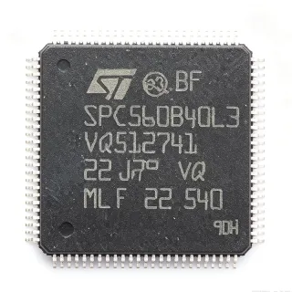
STM32F429VET6 - 180MHz Cortex-M4 MCU, 512KB Flash, LQFP-100 | STMicroelectronics
Teilenummer: STM32F429VET6 ✓ Aktiv| Menge | Stückpreis | Gesamt |
|---|---|---|
| 1 | $14.5 | $14,50 |
| 10 | $13.05 | $130,50 |
| 100 | $11.62 | $1.162,00 |
| 500 | $10.43 | $5.215,00 |
| 1.000 | $9.21 | $9.210,00 |
STM32F429VET6 Übersicht
What is an MCU? A microcontroller (MCU) is a single-chip computer that integrates a CPU core, program and data memory, peripherals, and I/O. The Cortex-M4 family from Arm is optimized for deterministic real-time embedded workloads with a single-precision FPU and a subset of DSP instructions (MAC, SIMD), making it the mid-tier workhorse for motor control, audio, connectivity, and graphical HMIs. The STM32F4 series specifically targets high clock frequencies (180 MHz), large SRAM, and rich connectivity (USB OTG HS/FS, Ethernet, CAN, SDIO, FMC) at mainstream cost points.
Key features include an Adaptive Real-Time (ART) Accelerator allowing 0-wait-state execution from Flash, a Cryptographic hash / AES-128 / RNG suite on the F429 line, Chrom-ART Accelerator for 2D graphics, and a TFT-LCD controller with SVGA support. The device offers USB OTG Full-Speed and High-Speed (with on-chip PHY on HS), 10/100 Ethernet MAC, 17 timers, three 12-bit ADCs (2.4 MSPS), two 12-bit DACs, and up to 20 communication interfaces including USART, SPI, I2C, CAN, and SAI.
The Cortex-M4 core uses a 3-stage pipeline with branch speculation, and the on-chip ART accelerator uses a 64-bit-wide Flash interface and user-configurable prefetch buffers, allowing the F429 to execute code from Flash at full 180 MHz without stalls. The Chrom-ART accelerator offloads 2D block transfers and pixel-format conversions from the CPU, freeing MIPS for application logic; the integrated TFT-LCD controller can drive displays up to SVGA resolution (800x600) over an 8080/6800 or HDMI-CEC/parallel-DSI bridge path.
Typical applications include graphical HMI panels (appliance, HVAC, medical, industrial), USB-connected test instruments, motor-control inverter boards, Ethernet-connected PLCs, and small-form-factor camera devices. The 1.8V core with on-chip regulator + integrated SDIO simplifies SD-card data logging. Design considerations: route the USB DP/DM pair as 90 ohm differential, place decoupling within 5 mm of each VDD pin, and use the on-chip LDO (PWR_REG) with a 1uF + 100nF capacitor network. The 100-pin LQFP has a thermal resistance of approximately 50 C/W (typical, per package), so at 180 MHz the device is comfortably within thermal limits below 70 C ambient. This page synthesizes distributor pricing, drop-in pin-compatible alternatives, and practical design notes beyond what the manufacturer datasheet alone provides.
Drop-in-Alternativen für STM32F429VET6 – gleiches Gehäuse, Pin-kompatibel. Bauteile mit anderem Gehäuse, die eine PCB-Überarbeitung erfordern, sind ausgeschlossen.
Varianten dieser Serie
Modelle derselben Serie, die drop-in-kompatibel sind mit STM32F429VET6 (gleiche Bauform und Footprint) – abweichend in SRAM, ADC, Package, Communication Interfaces, Operating Temperature.
Schnellvergleichstool – Wählen Sie Alternativbauteile für den Direktvergleich:
STM32F429VGT6
✅ Drop-In📋 Referenzalternative (nicht im Katalog)
STM32F427VGT6
✅ Drop-In✓ Auf Lager
$8.95 / Stück
Datenblatt ansehen →STM32F429VET6TR
✅ Drop-In📋 Referenzalternative (nicht im Katalog)
STM32F407VET6
✅ Drop-In✓ Auf Lager
$3.6094 / Stück
Datenblatt ansehen →GD32F450VKT6
✅ Drop-In📋 Referenzalternative (nicht im Katalog)
STM32F429VET6 Grenzwerte & elektrische Eigenschaften
| Core | Arm 32-bit Cortex-M4 with FPU |
| DSP Instructions | Yes |
| Maximale Taktfrequenz | 180 MHz |
| DMIPS | 225 DMIPS / 1.25 DMIPS per MHz (Dhrystone 2.1) |
| Program Flash | 512 KB |
| SRAM | 256 KB + 4 KB backup |
| Gehäuse | LQFP-100 (14x14 mm) |
| Versorgungsspannung | 1.8 V to 3.6 V |
| Betriebstemperatur | -40C to +85C (industrial grade) |
| USB | USB OTG Full-Speed + USB OTG High-Speed (on-chip PHY) |
| Ethernet | 10/100 MAC (external PHY required) |
| TFT-LCD Controller | Yes (up to SVGA 800x600) |
| Camera Interface | 8- to 14-bit parallel |
| ADC | 3x 12-bit, 2.4 MSPS |
| DAC | 2x 12-bit |
| Timers | 17 (incl. PWM, HRTIM on some SKUs) |
| Communication Interfaces | Up to 20 (USART/SPI/I2C/CAN/SAI/SDIO) |
| Crypto | AES-128, Hash, RNG |
| RoHS-Status | Compliant |
| Montageart | Surface Mount (LQFP) |
STM32F429VET6 Pin-Konfiguration
| Pin 1 | PE2 — GPIO PE2, TRACECLK |
| Pin 2 | PE3 — GPIO PE3, TRACED0 |
| Pin 3 | PE4 — GPIO PE4, TRACED1 |
| Pin 4 | PE5 — GPIO PE5, TRACED2 |
| Pin 5 | PE6 — GPIO PE6, TRACED3 |
| Pin 6 | VBAT — Backup battery / RTC domain |
| Pin 7 | PC13 — GPIO PC13, RTC TAMPER |
| Pin 8 | PC14 — GPIO PC14, OSC32_IN |
| Pin 9 | PC15 — GPIO PC15, OSC32_OUT |
| Pin 10 | VSS — Ground |
| Pin 11 | VDD — Digital supply |
| Pin 12 | PH0 — GPIO PH0, OSC_IN |
| Pin 13 | PH1 — GPIO PH1, OSC_OUT |
| Pin 14 | NRST — Reset, active low |
| Pin 15 | PC0 — GPIO PC0, ADC123_IN10 |
| Pin 16 | PC1 — GPIO PC1, ADC123_IN11 |
| Pin 17 | PC2 — GPIO PC2, ADC123_IN12 |
| Pin 18 | PC3 — GPIO PC3, ADC123_IN13 |
| Pin 19 | VSSA — Analog ground |
| Pin 20 | VREF+ — ADC reference voltage positive |
| Pin 21 | VDDA — Analog supply |
| Pin 22 | PA0 — GPIO PA0, WKUP, UART4_TX, TIM5_CH1 |
| Pin 23 | PA1 — GPIO PA1, UART4_RX, TIM5_CH2, ETH_RMII_REF_CLK |
| Pin 24 | PA2 — GPIO PA2, USART2_TX, TIM5_CH3, ETH_MDIO |
| Pin 25 | PA3 — GPIO PA3, USART2_RX, TIM5_CH4, ETH_MII_COL |
| Pin 26 | VSS — Ground |
| Pin 27 | VDD — Digital supply |
| Pin 28 | PA4 — GPIO PA4, SPI1_NSS, USART2_CK, ADC12_IN4, ETH_MII_RXD0 |
| Pin 29 | PA5 — GPIO PA5, SPI1_SCK, ADC12_IN5, ETH_MII_RXER |
| Pin 30 | PA6 — GPIO PA6, SPI1_MISO, ADC12_IN6, TIM8_BKIN, ETH_MII_RX_DV |
| Pin 31 | PA7 — GPIO PA7, SPI1_MOSI, ADC12_IN7, ETH_MII_RX_CLK |
| Pin 32 | PC4 — GPIO PC4, ETH_MII_RXD0/RMII_RXD0 |
| Pin 33 | PC5 — GPIO PC5, ETH_MII_RXD1/RMII_RXD1 |
| Pin 34 | PB0 — GPIO PB0, ADC12_IN8, ETH_MII_RXD2, TIM3_CH3 |
| Pin 35 | PB1 — GPIO PB1, ADC12_IN9, ETH_MII_RXD3, TIM3_CH4 |
| Pin 36 | PB2 — GPIO PB2, BOOT1 |
| Pin 37 | PE7 — GPIO PE7, TIM1_ETR |
| Pin 38 | PE8 — GPIO PE8, TIM1_CH1N |
| Pin 39 | PE9 — GPIO PE9, TIM1_CH1 |
| Pin 40 | PE10 — GPIO PE10, TIM1_CH2N |
| Pin 41 | PE11 — GPIO PE11, TIM1_CH2 |
| Pin 42 | PE12 — GPIO PE12, TIM1_CH3N |
| Pin 43 | PE13 — GPIO PE13, TIM1_CH3 |
| Pin 44 | PE14 — GPIO PE14, TIM1_CH4 |
| Pin 45 | PE15 — GPIO PE15, TIM1_BKIN |
| Pin 46 | PB10 — GPIO PB10, I2C2_SCL, USART3_TX, ETH_MII_RX_ER |
| Pin 47 | PB11 — GPIO PB11, I2C2_SDA, USART3_RX, ETH_MII_TX_EN/RMII_TX_EN |
| Pin 48 | VCAP_1 — Internal LDO bypass (1.8 V core) |
| Pin 49 | VSS — Ground |
| Pin 50 | VDD — Digital supply |
| Pin 51 | PB12 — GPIO PB12, SPI2_NSS, I2S2_WS, TIM1_BKIN, ETH_MII_TXD0 |
| Pin 52 | PB13 — GPIO PB13, SPI2_SCK, I2S2_CK, ETH_MII_TXD1 |
| Pin 53 | PB14 — GPIO PB14, SPI2_MISO, I2S2ext_SD, TIM8_CH2N |
| Pin 54 | PB15 — GPIO PB15, SPI2_MOSI, I2S2_SD, TIM8_CH3N |
| Pin 55 | PD8 — GPIO PD8, USART3_TX, ETH_MII_RXD3 |
| Pin 56 | PD9 — GPIO PD9, USART3_RX, ETH_MII_RXD2 |
| Pin 57 | PD10 — GPIO PD10, FSMC_NOE/EVENTOUT |
| Pin 58 | PD11 — GPIO PD11, FSMC_A16, USART3_CTS |
| Pin 59 | PD12 — GPIO PD12, FSMC_A17, TIM4_CH1, USART3_RTS |
| Pin 60 | PD13 — GPIO PD13, FSMC_A18, TIM4_CH2 |
| Pin 61 | PD14 — GPIO PD14, FSMC_D0, TIM4_CH3 |
| Pin 62 | PD15 — GPIO PD15, FSMC_D1, TIM4_CH4 |
| Pin 63 | PC6 — GPIO PC6, I2S2_MCK, TIM8_CH1, USART6_TX, FSMC_NWAIT |
| Pin 64 | PC7 — GPIO PC7, I2S3_MCK, TIM8_CH2, USART6_RX, FSMC_NE1 |
| Pin 65 | PC8 — GPIO PC8, TIM8_CH3, USART6_CK, FSMC_NCE2 |
| Pin 66 | PC9 — GPIO PC9, TIM8_CH4, I2C3_SDA, I2S_CKIN |
| Pin 67 | PA8 — GPIO PA8, I2C3_SCL, USART1_CK, TIM1_CH1, OTG_FS_SOF, MCO1 |
| Pin 68 | PA9 — GPIO PA9, I2C3_SMBA, USART1_TX, TIM1_CH2, OTG_FS_VBUS |
| Pin 69 | PA10 — GPIO PA10, USART1_RX, TIM1_CH3, OTG_FS_ID |
| Pin 70 | PA11 — GPIO PA11, CAN1_RX, USART1_CTS, TIM1_CH4, OTG_FS_DM |
| Pin 71 | PA12 — GPIO PA12, CAN1_TX, USART1_RTS, TIM1_ETR, OTG_FS_DP |
| Pin 72 | PA13 — GPIO PA13, JTMS-SWDIO |
| Pin 73 | VCAP_2 — Internal LDO bypass |
| Pin 74 | VSS — Ground |
| Pin 75 | VDD — Digital supply |
| Pin 76 | PA14 — GPIO PA14, JTCK-SWCLK |
| Pin 77 | PA15 — GPIO PA15, JTDI, SPI3_NSS, I2S3_WS, TIM2_CH1 |
| Pin 78 | PC10 — GPIO PC10, SPI3_SCK, I2S3_CK, UART4_TX, FSMC_NE3 |
| Pin 79 | PC11 — GPIO PC11, SPI3_MISO, I2S3ext_SD, UART4_RX, FSMC_NCE4_1 |
| Pin 80 | PC12 — GPIO PC12, SPI3_MOSI, I2S3_SD, UART5_TX, FSMC_NCE4_2 |
| Pin 81 | PD0 — GPIO PD0, CAN1_RX, FSMC_D2 |
| Pin 82 | PD1 — GPIO PD1, CAN1_TX, FSMC_D3 |
| Pin 83 | PD2 — GPIO PD2, SDIO_CMD, TIM3_ETR, UART5_RX |
| Pin 84 | PD3 — GPIO PD3, SDIO_CLK, FSMC_CLK |
| Pin 85 | PD4 — GPIO PD4, USART2_RTS, FSMC_NOE |
| Pin 86 | PD5 — GPIO PD5, USART2_TX, FSMC_NWE |
| Pin 87 | PD6 — GPIO PD6, USART2_RX, FSMC_NWAIT |
| Pin 88 | PD7 — GPIO PD7, USART2_CK, FSMC_NCE2 |
| Pin 89 | PB3 — GPIO PB3, JTDO, SPI3_SCK, I2S3_CK, TIM2_CH2, SWO |
| Pin 90 | PB4 — GPIO PB4, NJTRST, SPI3_MISO, I2S3ext_SD, TIM3_CH1 |
| Pin 91 | PB5 — GPIO PB5, SPI3_MOSI, I2S3_SD, CAN2_RX, TIM3_CH2 |
| Pin 92 | PB6 — GPIO PB6, I2C1_SCL, CAN2_TX, TIM4_CH1, USART1_TX |
| Pin 93 | PB7 — GPIO PB7, I2C1_SDA, TIM4_CH2, USART1_RX |
| Pin 94 | BOOT0 — Boot mode select (Flash / System ROM) |
| Pin 95 | PB8 — GPIO PB8, I2C1_SCL, CAN1_RX, TIM4_CH3, SDIO_D4 |
| Pin 96 | PB9 — GPIO PB9, I2C1_SDA, CAN1_TX, TIM4_CH4, SDIO_D5 |
| Pin 97 | PE0 — GPIO PE0, TIM4_ETR, FSMC_NBL0 |
| Pin 98 | PE1 — GPIO PE1, FSMC_NBL1 |
| Pin 99 | VSS — Ground |
| Pin 100 | VDD — Digital supply |
Typische Anwendungen
STM32F429VET6 ist geeignet für 7 Anwendungs: Graphical HMI Panel (TFT-LCD Touch UI), Industrial Motor Control / FOC Drive, Industrial Ethernet Gateway / PLC, USB Test & Measurement Instrument, Camera-Enabled Embedded Vision Device, Audio Playback / DSP Effects Processor, IoT Edge Node with Secure Boot.
Graphical HMI Panel (TFT-LCD Touch UI)
The STM32F429VET6's integrated TFT-LCD controller (up to SVGA 800x600) and the Chrom-ART 2D accelerator remove the need for an external graphics controller in HMI boards, reducing BOM cost and PCB area. Designers can drive displays like a 7-inch 800x480 RGB-TFT directly from the controller's parallel interface with on-chip frame-buffer in 256 KB SRAM, leaving the Cortex-M4 at 180 MHz for UI logic. The hardware crypto and RNG blocks also let the device run secure boot and TLS handshakes for network-connected appliances. Compared with the STM32F407 family the F429's on-chip TFT controller saves 1-2 USD and 200 mm² of board space per design.
Empfohlen
Industrial Motor Control / FOC Drive
The STM32F429VET6 is well-suited for field-oriented control (FOC) of 3-phase PMSM and BLDC motors thanks to its 6-channel advanced-control PWM timers with programmable dead-time insertion. The 12-bit ADC reaches 2.4 MSPS, and in dual-interleaved mode 4.7 MSPS, so a single-shunt current-sense stage can resolve a 50 kHz PWM drive per ST application note AN3150. Designers typically pair the MCU with ST's STGIPN3H60 gate driver and a 5 kW SiC inverter, leveraging the F429's 256 KB SRAM for sensorless observer state-variables. The Cortex-M4 FPU accelerates Park/Clarke transforms by ~40% over the Cortex-M3 generation.
Empfohlen
Industrial Ethernet Gateway / PLC
The STM32F429VET6 integrates a 10/100 Ethernet MAC that - combined with the on-chip USB-OTG and SDIO - lets designers build compact industrial gateways that bridge sensor networks (Modbus/TCP, EtherNet/IP) to backhaul uplinks. Real-time FreeRTOS + LwIP stacks run comfortably on 256 KB SRAM with the FPU accelerating JSON/XML parsing. The MCU's 1.8-3.6V range and -40 to +85C industrial operating temperature make it acceptable for PLC chassis. Designers typically add an external LAN8720A RMII PHY, plus eMMC/SD card through SDIO for local data buffering.
Empfohlen
USB Test & Measurement Instrument
Engineers building USB-connected oscilloscopes, logic analyzers, or data-acquisition modules benefit from the STM32F429VET6's dual USB OTG controllers: the high-speed 480 Mb/s channel gives ample bandwidth for streaming ADC data, while the full-speed OTG can act as a USB-C Power Delivery sink. The 12-bit ADC at 2.4 MSPS plus a single-precision FPU performs FFTs and digital-filtering in real time at sample rates under 100 kS/s. A complete 4-channel 1 MS/s scope is achievable inside the 512 KB Flash with ST's open-source oscilloscope firmware. The hardware crypto (AES-128) secures the USB control channel between the instrument and the host PC.
Empfohlen
Camera-Enabled Embedded Vision Device
The STM32F429VET6 has an 8- to 14-bit parallel camera interface (DCMI) that accepts raw Bayer-RGB data from OV5640-class CMOS sensors at up to 14 MB/s in burst mode. With Chrom-ART accelerating JPEG-decompression and the FPU doing 3-channel demosaicing, the F429 performs simple machine-vision tasks (color blob detection, frame differencing) at VGA 30 fps. The integrated TFT-LCD controller can preview the image directly on a 800x480 RGB-TFT without an external bridge. For higher resolution, designers move to STM32N6 with a dedicated NPU; for this class the F429 offers an unbeatable cost-per-vision-pipeline ratio.
Empfohlen
Audio Playback / DSP Effects Processor
The SAI (Serial Audio Interface) plus the SAI PDM/SAI SPDIF interfaces make the STM32F429VET6 an excellent host for audio effects, USB speakers, or in-car infotainment sub-modules. Sampling rates up to 96 kHz at 24-bit are easily handled by the FPU doing biquad filters, reverb tails, and dynamics. The integrated USB OTG-HS delivers a high-bandwidth audio class 2.0 stream to the host PC. Designers often pair the F429 with an external audio DAC like the PCM1794A via I2S, leaving the Cortex-M4 cores ~50% utilization for stream decoding. The 1.8-3.6V supply simplifies battery-powered portable audio gear.
Empfohlen
IoT Edge Node with Secure Boot
The STM32F429VET6's hardware AES-128, SHA-1/SHA-2 hash, and true RNG blocks accelerate TLS 1.2/1.3 handshakes on Cortex-M4, achieving TLS handshake in ~150 ms on real hardware per ST application note AN4235. Secure-boot firmware verifies signatures in < 50 ms because AES decryption runs as a single-cycle instruction. Designers integrate LwIP or MBED TLS over the on-chip Ethernet MAC, or Wi-Fi via SPI-controlled modules. The 4 KB backup SRAM offers RTC-grade key storage while the device is in standby at 1.8 uA typical. The 100-LQFP footprint eases reflow and rework in tightly stacked sensor boards.
Empfohlen
Zusammenfassung der empfohlenen Produkte
Technische Referenzdaten für STM32F429VET6 – Vergleich, Designhinweise und Compliance-Informationen.
Auswahlhilfe
Vergleich mit Alternativen
| Parameter | Dieses Produkt | STM32F429VGT6 | STM32F427VGT6 | STM32F407VET6 | GD32F450VKT6 |
|---|---|---|---|---|---|
| Brand | STMicroelectronics | STMicroelectronics | STMicroelectronics | STMicroelectronics | GigaDevice |
| Package | LQFP-100 (14x14 mm) | LQFP-100 - same | LQFP-100 - same | LQFP-100 - same | LQFP-100 - same |
| Core / Max Clock | Cortex-M4 / 180 MHz | Cortex-M4 / 180 MHz (same) | Cortex-M4 / 180 MHz (same) | Cortex-M4 / 180 MHz (same) | Cortex-M4 / 200 MHz (+11%) |
| Flash | 512 KB | 1 MB (+100%) | 1 MB (+100%) | 512 KB (same) | 2 MB (+300%) |
| SRAM | 256 KB + 4 KB backup | 256 KB + 4 KB (same) | 256 KB + 4 KB (same) | 192 KB + 4 KB (-25%) | 256 KB (same, no backup) |
| TFT-LCD Controller | Yes (SVGA 800x600) | Yes (same) | No (F427L only) | No | Yes |
| USB OTG | FS + HS (on-chip PHY) | FS + HS (same) | FS + HS (same) | FS + HS (same) | FS + HS (same) |
| Ethernet MAC | 10/100 (MII/RMII) | 10/100 (same) | 10/100 (same) | 10/100 (same) | 10/100 (same) |
| Hardware Crypto (AES / RNG / Hash) | AES-128, RNG, SHA-1/2 | Same | RNG only | None | AES-256, RNG, SHA only |
| Approx. Unit Price (qty-1 USD) | ~14.50 | ~17.00 | ~17.50 | ~13.00 | ~6.50 |
Wichtigste Unterscheidungsmerkmale
- On-chip TFT-LCD controller and Chrome-ART 2D accelerator (vs. STM32F407VET6)
- Hardware AES-128 and RNG included (vs. GD32F450VKT6)
- Mature STM32CubeF4 ecosystem (vs. GD32F450VKT6)
Designhinweise
Provide a 100 nF X7R ceramic on each VDD/VSS pair placed within 5 mm of the pins, plus a 4.7 uF bulk capacitor on the regulator output (e.g. AP2112-3.3 SOT-23-5) before VCAP pins. Estimated: at 180 MHz with all peripherals disabled the F429VET6 typically draws ~70 mA (per ST DS-table for typical TFBGA-grade silicon), but with USB HS, Ethernet, and TFT-LCD active draw climbs to 130 mA. The internal VCAP_1 and VCAP_2 rails each need a 1 uF + 100 nF parallel network with 2 nH ESR; do not share their capacitance. VDD must be in the 1.8-3.6 V window; monitor VDD with the brown-out-reset (BOR) to avoid Flash corruption.
The LQFP-100 with 4-layer 2-oz copper PCB has typical theta_JA around 50 C/W (per ST PM0075 package thermal note). Estimated: at 130 mA and 3.3 V dissipation is 0.43 W, giving a self-heating of ~21 C above ambient, well inside the 85 C industrial ceiling. For -40C to +105C industrial designs increase the copper pour to 1-oz area of 2 sq-cm to keep margin. The LQFP body is plastic so avoid mechanical mounting near parts that need to be cooler than the MCU.
Route the USB OTG-HS DP/DM pair as 90-ohm differential over an unbroken ground reference, max 8 mm trace length mismatch (per AN5457). Place the 1.5 kohm pull-up and 22-ohm series resistor near the connector, and series-common-mode choke (e.g. ACM2012) at the cable entry. The Ethernet RMII signals to an external LAN8720A need 50-ohm trace impedance and length-matched + within 50 mm of the PHY; keep the 50 MHz RMII_REF_CLK trace to one layer and surround with ground stitches. Pin-out the SDIO bus as parallel matched-length lines to avoid timing violations at 50 MHz SDHC. The LQFP-100 has 0.5 mm pitch and benefits from 6/6 mil trace/space rules on the inner PCB layers.
Common pitfalls include: (1) Over-driving the USB HS DP/DM without a 45-ohm RC network - causes FATAL USB compliance failure. (2) Forgetting to set ART Accelerator ACR[PRFTEN] before clocking above 84 MHz, which halves Flash throughput. (3) Using the FPU interrupt handlers without saving floating-point state on the stack (lazy stacking) leads to CRASHES - consult device errata ES0287 for the complete list. (4) Using the same SDIO pin mapping as the F407 and the F429 at the same time - the F429 TFT-LCD controller occupies those pins, causing conflicts. (5) Trying to use 5 V GPIOs into the F429 - the I/O is 5V-tolerant on TT pins only, never stretch 5V into a regular pin.
Compliance-Informationen
RoHS and REACH compliant per Mouser/DigiKey listings. Halogen-free per ST product environmental compliance docs. Not AEC-Q100 qualified; for automotive applications consider STM32F429VET6-ANT (industrial grade) or upgrade to STM32F429NIH6/H7 derivatives. Conflict-mineral reporting per ST's CMRT filings.