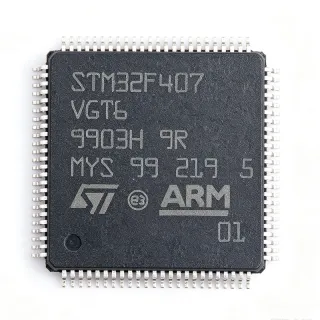
STM32F407VET6 - 168MHz Cortex-M4 MCU 512KB Flash | ST
MPN: STM32F407VET6 ✓ Active| Qty | Unit Price | Extended |
|---|---|---|
| 1 | $9.6 | $9.60 |
| 10 | $8.7 | $87.00 |
| 100 | $7.9 | $790.00 |
| 500 | $7.2 | $3,600.00 |
| 1,000 | $6.6 | $6,600.00 |
STM32F407VET6 Overview
What is a microcontroller? A microcontroller (MCU) is a single-chip integrated circuit that combines a processor core, memory (Flash and SRAM), and programmable peripherals to govern specific operations in embedded systems. The STM32F407VET6 belongs to the STM32F4 series built on the ARM Cortex-M4 core with a floating-point unit (FPU) and DSP instructions, positioned within the broader hierarchy of 32-bit MCUs for real-time control and signal processing.
Key features include a 168 MHz Cortex-M4F core, 512 KB Flash, 192 KB SRAM, an Ethernet MAC, USB OTG HS/FS, a camera interface (DCMI), three 12-bit ADCs with up to 16 channels, dual 12-bit DACs, and advanced timers plus USART, SPI, I2C, and CAN communication interfaces. The supply range is 1.8V to 3.6V with operation from -40C to +85C.
Technically, the device uses a 90nm process and a Harvard bus architecture with separate instruction and data buses for simultaneous memory access. A memory protection unit (MPU) and nested vectored interrupt controller (NVIC) support deterministic real-time behavior, while the single-precision FPU accelerates math-intensive firmware.
Typical applications include industrial control and motor drives, networked IoT gateways using the on-chip Ethernet MAC, and machine-vision or imaging systems leveraging the DCMI camera interface.
Design tip: decouple all VDD pins with 100nF ceramics plus bulk capacitance, keep VDDA/VSSA on a clean analog supply to minimize ADC noise, and pay careful attention to HSE crystal layout for stable clocking.
Drop-in alternatives for STM32F407VET6 — same package, pin-to-pin compatible. Different-package parts requiring PCB rework are excluded.
Variants in this series
Same-series models that are drop-in compatible with STM32F407VET6 (same form factor and footprint) — differing in ADC, Camera Interface, Communication Interfaces, Core, Flash Memory.
Quick Comparison Tool — Select alternative parts for side-by-side comparison:
STM32F407VGT6
✅ Drop-In✓ In Stock
$7.55 / Unit
View Datasheet →STM32F405VET6
✅ Drop-In ⚠️ 参数待验证📋 Reference alternative (not in catalog)
STM32F407VET7
✅ Drop-In ⚠️ 参数待验证📋 Reference alternative (not in catalog)
GD32F407VET6
✅ Drop-In📋 Reference alternative (not in catalog)
AT32F407VET7
✅ Drop-In📋 Reference alternative (not in catalog)
STM32F407VET6 Maximum Ratings & Electrical Characteristics
| Core | ARM Cortex-M4 32-bit with FPU |
| Maximum Clock Frequency | 168 MHz |
| Flash Memory | 512 KB |
| SRAM | 192 KB |
| Supply Voltage | 1.8 V to 3.6 V |
| Operating Temperature | -40C to +85C |
| Package | LQFP-100 (14x14 mm) |
| Mounting Style | SMD/SMT |
| Data Bus Width | 32 bit |
| ADC | 3x 12-bit, up to 16 channels |
| DAC | 2x 12-bit |
| Ethernet | 10/100 MAC |
| USB | OTG HS + OTG FS |
| Camera Interface | DCMI |
| Communication Interfaces | USART, SPI, I2C, CAN, SDIO |
| Process Technology | 90 nm |
| RoHS Status | Compliant |
STM32F407VET6 Pin Configuration
| Pin 12 | VDD — Digital supply 1.8V-3.6V |
| Pin 13 | VSS — Digital ground |
| Pin 19 | VDDA — Analog supply for ADC/DAC |
| Pin 18 | VSSA — Analog ground |
| Pin 5 | OSC_IN — HSE crystal input |
| Pin 6 | OSC_OUT — HSE crystal output |
| Pin 14 | NRST — Active-low reset |
| Pin 94 | BOOT0 — Boot mode selection |
| Pin 72 | PA0-WKUP — ADC input / wake-up |
| Pin 37 | PA9 — USART1_TX |
| Pin 38 | PA10 — USART1_RX |
| Pin 29 | PA5 — SPI1_SCK / DAC2 output |
Typical Applications
STM32F407VET6 is suitable for 6 applications: Industrial Control and Automation, Motor Drives, IoT Gateway and Networking, Machine Vision and Imaging, Medical and Diagnostic Devices, Consumer and HMI Devices.
Industrial Control and Automation
The STM32F407VET6 fits industrial control nodes where 168 MHz real-time processing, multiple CAN and UART channels, and deterministic interrupt handling are required. The NVIC and MPU enable hard-real-time task scheduling, while advanced timers generate complementary PWM with dead-time insertion for drives. Its -40C to +85C rating and 1.8V-3.6V operation suit factory-floor conditions. With 512 KB Flash, control logic plus protocol stacks coexist in one chip, and dual watchdogs protect uptime.
Recommended
Motor Drives
The STM32F407VET6 is well suited to FOC and sensorless motor control: its 168 MHz Cortex-M4F with FPU closes current loops fast enough for 20 kHz+ PWM, and three 12-bit ADCs sample phase currents with injected conversions synchronized to timer triggers. Complementary PWM outputs with dead-time insertion drive three-phase inverters via gate drivers. The 512 KB Flash stores field weakening and protection algorithms alongside the control loop without external memory.
Recommended
IoT Gateway and Networking
With an integrated 10/100 Ethernet MAC, the STM32F407VET6 forms compact networked gateways when paired with an external PHY such as the DP83TD555J-Q1. The 192 KB SRAM accommodates TCP/IP stacks and TLS buffers, while SPI and USART links connect radio modules or sensors. USB OTG FS provides device configuration and field updates. Running LwIP at 168 MHz yields line-rate bridging for 10/100 traffic, making it ideal for smart-metering and building-automation concentrators.
Recommended
Machine Vision and Imaging
The DCMI camera interface of the STM32F407VET6 connects directly to CMOS image sensors, streaming 8-14 bit parallel video data with DMA into 192 KB SRAM or external memory. At 168 MHz, the Cortex-M4F with DSP instructions performs histogram, edge-detection, and basic pixel processing on-line, while the FPU accelerates lens-correction math. Image sensors such as the AR0821CS class devices interface through the DCMI for inspection and barcode applications.
Recommended
Medical and Diagnostic Devices
The STM32F407VET6 supports portable medical instruments where three 12-bit ADCs digitize physiological signals with up to 2.4 MSPS, and the 32-bit DSP engine runs filtering and FFT analysis. USB OTG and Ethernet enable data upload to clinic systems, while the -40C to +85C range and low 1.8V-3.6V operation suit battery-powered designs. A precision reference and low-noise amplifiers such as the OPA211 preserve signal integrity ahead of the ADC inputs.
Recommended
Consumer and HMI Devices
For smart appliances, printers, and human-machine interfaces, the STM32F407VET6 drives TFT panels over FSMC and reads touch through I2C, while USB OTG FS handles accessories and firmware updates. The 168 MHz Cortex-M4F renders simple UI graphics and audio prompts, and 512 KB Flash holds localization assets and BLE/Wi-Fi module stacks communicated over USART. Volume availability and second-source pin-compatible options reduce supply risk in consumer BOMs.
Recommended
Recommended Products Summary
Engineering reference data for STM32F407VET6 — comparison, design guidance, and compliance information.
Selection Guide
Comparison with Alternatives
| Parameter | This Product | STM32F407VGT6 | STM32F405VET6 | GD32F407VET6 | AT32F407VET7 |
|---|---|---|---|---|---|
| Package | LQFP-100 (14x14 mm) | LQFP-100 - same | LQFP-100 - same | LQFP-100 - same | LQFP-100 - same |
| Brand | STMicroelectronics | STMicroelectronics | STMicroelectronics | GigaDevice | Artery Technology |
| Core / Frequency | Cortex-M4F, 168 MHz | Cortex-M4F, 168 MHz | Cortex-M4F, 168 MHz | Cortex-M4F, 168 MHz | Cortex-M4F, 168 MHz |
| Flash Memory | 512 KB | 1024 KB | 512 KB | 512 KB | 512 KB |
| Ethernet MAC | Yes (10/100) | Yes (10/100) | No | Yes (10/100) | Yes (10/100) |
| Firmware Compatibility | Reference (STM32 HAL) | Full STM32 HAL compatibility | Compatible except Ethernet | Mostly compatible, validation needed | Porting required |
Key Differentiators
- Integrated 10/100 Ethernet MAC (vs STM32F405VET6)
- 512 KB Flash at lower cost (vs STM32F407VGT6)
- Mature STM32 ecosystem (vs GD32F407VET6)
Design Notes
Decouple every VDD pin pair with 100nF ceramic capacitors placed within 2mm of the pins, plus one 4.7uF bulk capacitor. Keep VDDA on a separate filtered supply (ferrite bead + 1uF + 10nF) to prevent digital switching noise from degrading the 12-bit ADC; ST AN4207 provides the recommended supply topology.
Route the HSE crystal (4-26 MHz) with short traces, guard with ground, and keep load capacitors close to pins 5/6. BOOT0 must be tied through a 10k resistor to GND for normal flash boot. The 100-pin LQFP with 0.5mm pitch requires careful solder-paste stencil design to avoid bridging.
Do not exceed 3.6V on VDD or 5V tolerance assumptions on PA/PC pins - only FT (five-volt-tolerant) pins accept 5V signals. Ethernet requires an external PHY and 25MHz reference; it is not plug-and-play. When porting to GD32F407VET6 or AT32F407VET7 substitutes, validate flash wait-states and USB timing before release.
Compliance Information
RoHS compliant and lead-free per ST product data. REACH/halogen/conflict-mineral declarations not found in provided data.