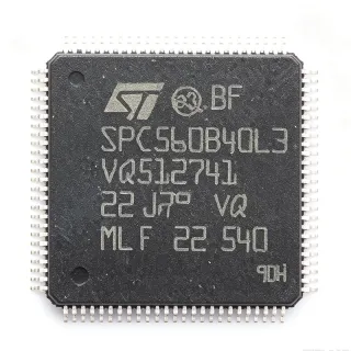
STM32G474VET3 - 170MHz Cortex-M4F MCU 512KB LQFP-100 | ST
Teilenummer: STM32G474VET3 ✓ Aktiv| Menge | Stückpreis | Gesamt |
|---|---|---|
| 1 | $7.3 | $7,30 |
| 10 | $6.85 | $68,50 |
| 100 | $6.1 | $610,00 |
| 500 | $5.55 | $2.775,00 |
| 1.000 | $5 | $5.000,00 |
STM32G474VET3 Übersicht
An Arm Cortex-M4 microcontroller is a 32-bit RISC processor core designed for deterministic real-time embedded control, with single-precision floating-point, DSP extensions, and a tightly-coupled NVIC for low-latency interrupt handling. Within the broader taxonomy, this part belongs to the MCU -> microcontroller -> semiconductor category, and to ST's STM32G4 series, which adds a CORDIC math accelerator and FMAC filter-math accelerator that offload trigonometric and FIR/IIR computations from the CPU for digital power conversion and motor-control loops.
Key features include five 12-bit ADCs sampling at 4 MSPS with hardware oversampling to 16-bit effective resolution, four 12-bit DAC channels, seven comparators, six op-amps with programmable gain, four 184 ps resolution high-resolution timer channels, USB 2.0 Full-speed with PHY, CAN-FD, three SPI, three I2C, two UART/LPUART, an SDMMC package interface, and a math accelerator block (CORDIC + FMAC). The 100-LQFP exposes 81 GPIO across five voltage-tolerant 5V-tolerant I/O banks.
The STM32G474 architecture pairs the Cortex-M4F core with ST's adaptive real-time ART Accelerator and a multi-bank Flash controller that delivers zero-wait-state execution from Flash at 170 MHz. The integrated op-amps and comparators are tightly coupled to the high-resolution timer to form current-shunt and BEMF sensing loops without external analog ICs, enabling compact, BOM-light field-oriented-control (FOC) motor drives and LLC/PSFB digital power stages.
Typical applications include digital switched-mode power supplies (LLC, PSFB, totem-pole PFC), field-oriented-control motor drives for industrial servos and e-bikes, solar inverters and battery management, USB-C PD controllers, LED lighting controllers, and industrial sensor hubs. The math accelerator is particularly valuable in these loops because CORDIC evaluates sin/cos/atan in as few as 15 cycles.
When designing with this device, place a 100 nF decoupling capacitor on each VDD pin within 2 mm of the package, plus a 4.7 uF bulk cap on the regulator input. Reserve PB8/PB9 for the bootloader or ensure they are not pulled low at reset if you intend to boot from Flash.
This page synthesizes distributor pricing, drop-in alternatives, and practical design notes not found in the manufacturer datasheet. Engineers evaluating the STM32G474VET3 for a 100-LQFP design will find comparison data versus pin-compatible STM32G474xB/xC/xE siblings and GigaDevice GD32G5xx family cross-references here.
Drop-in-Alternativen für STM32G474VET3 – gleiches Gehäuse, Pin-kompatibel. Bauteile mit anderem Gehäuse, die eine PCB-Überarbeitung erfordern, sind ausgeschlossen.
Varianten dieser Serie
Modelle derselben Serie, die drop-in-kompatibel sind mit STM32G474VET3 (gleiche Bauform und Footprint) – abweichend in Comparators, Core, Operational Amplifiers, Package, Flash Memory.
Schnellvergleichstool – Wählen Sie Alternativbauteile für den Direktvergleich:
STM32G474VET6
✅ Drop-In✓ Auf Lager
$5.44 / Stück
Datenblatt ansehen →STM32G474VET3TR
✅ Drop-In📋 Referenzalternative (nicht im Katalog)
STM32G474RET6
✅ Drop-In✓ Auf Lager
$8.25 / Stück
Datenblatt ansehen →STM32G474CET6
✅ Drop-In✓ Auf Lager
$5.94 / Stück
Datenblatt ansehen →STM32G474CET3
✅ Drop-In📋 Referenzalternative (nicht im Katalog)
STM32G474RBT6
✅ Drop-In✓ Auf Lager
$3.7734 / Stück
Datenblatt ansehen →STM32G474RBT3
✅ Drop-In✓ Auf Lager
$2.84 / Stück
Datenblatt ansehen →STM32G474VET3 Grenzwerte & elektrische Eigenschaften
| Core | Arm Cortex-M4F with FPU and DSP |
| Maximale Taktfrequenz | 170 MHz |
| CoreMark / DMIPS | 213 DMIPS |
| Flash Memory | 512 KB |
| SRAM | 128 KB |
| Gehäuse | LQFP-100 (14x14 mm) |
| Operating Voltage | 1.71 V to 3.6 V |
| GPIO Count | 81 |
| ADC | 5x 12-bit, 4 MSPS, HW oversampling to 16-bit |
| DAC | 4x 12-bit |
| Comparators | 7 ultra-fast rail-to-rail |
| Operational Amplifiers | 6 internal op-amps with PGA |
| High-Resolution Timer | 4 channels, 184 ps resolution |
| Math Accelerator | CORDIC + FMAC |
| Communication Interfaces | USB 2.0 FS, CAN-FD, 3x SPI, 3x I2C, 2x UART/LPUART, SDMMC |
| Betriebstemperatur | -40C to +125C |
| Montageart | Surface Mount |
| RoHS-Status | Compliant |
STM32G474VET3 Pin-Konfiguration
| Pin 1 | PE2 — GPIO PE2 / TRACECLK |
| Pin 2 | PE3 — GPIO PE3 / TRACED0 |
| Pin 3 | PE4 — GPIO PE4 / TRACED1 |
| Pin 4 | PE5 — GPIO PE5 / TRACED2 |
| Pin 5 | PE6 — GPIO PE6 / TRACED3 |
| Pin 6 | VBAT — RTC backup battery supply |
| Pin 7 | PC13 — GPIO PC13 / TAMPER-RTC |
| Pin 8 | PC14 — GPIO PC14 / OSC32_IN |
| Pin 9 | PC15 — GPIO PC15 / OSC32_OUT |
| Pin 10 | VSS — Ground |
| Pin 11 | VDD — Digital supply voltage |
| Pin 12 | VREF+ — ADC/DAC reference voltage |
| Pin 13 | PA0 — GPIO PA0 / ADC1_INP1 / TIM2_CH1 |
| Pin 14 | PA1 — GPIO PA1 / ADC1_INP2 / TIM2_CH2 |
| Pin 15 | PA2 — GPIO PA2 / USART2_TX / ADC1_INP3 |
| Pin 16 | PA3 — GPIO PA3 / USART2_RX / ADC1_INP4 |
| Pin 17 | PA4 — GPIO PA4 / DAC1_OUT1 / SPI3_NSS |
| Pin 18 | PA5 — GPIO PA5 / DAC1_OUT2 / SPI3_SCK |
| Pin 19 | PA6 — GPIO PA6 / DAC2_OUT1 / SPI3_MISO |
| Pin 20 | PA7 — GPIO PA7 / DAC2_OUT2 / SPI3_MOSI |
| Pin 21 | PC4 — GPIO PC4 / ADC2_INP4 |
| Pin 22 | PC5 — GPIO PC5 / ADC2_INP5 |
| Pin 23 | PB0 — GPIO PB0 / ADC1_INP12 / TIM3_CH3 |
| Pin 24 | PB1 — GPIO PB1 / ADC1_INP11 / TIM3_CH4 |
| Pin 25 | PB2 — GPIO PB2 / BOOT1 |
| Pin 26 | PF11 — GPIO PF11 |
| Pin 27 | PF12 — GPIO PF12 |
| Pin 28 | VSS — Ground |
| Pin 29 | VDD — Digital supply voltage |
| Pin 30 | PE7 — GPIO PE7 |
| Pin 31 | PE8 — GPIO PE8 |
| Pin 32 | PE9 — GPIO PE9 / TIM1_CH1 |
| Pin 33 | PE10 — GPIO PE10 / TIM1_CH2N |
| Pin 34 | PE11 — GPIO PE11 / TIM1_CH2 |
| Pin 35 | PE12 — GPIO PE12 / TIM1_CH3N |
| Pin 36 | PE13 — GPIO PE13 / TIM1_CH3 |
| Pin 37 | PE14 — GPIO PE14 / TIM1_CH4 |
| Pin 38 | PE15 — GPIO PE15 / TIM1_BKIN |
| Pin 39 | PB10 — GPIO PB10 / I2C2_SCL |
| Pin 40 | PB11 — GPIO PB11 / I2C2_SDA |
| Pin 41 | VSS — Ground |
| Pin 42 | VDD — Digital supply voltage |
| Pin 43 | PB12 — GPIO PB12 / SPI2_NSS |
| Pin 44 | PB13 — GPIO PB13 / SPI2_SCK |
| Pin 45 | PB14 — GPIO PB14 / SPI2_MISO |
| Pin 46 | PB15 — GPIO PB15 / SPI2_MOSI |
| Pin 47 | PD8 — GPIO PD8 / USART3_TX |
| Pin 48 | PD9 — GPIO PD9 / USART3_RX |
| Pin 49 | PD10 — GPIO PD10 |
| Pin 50 | PD11 — GPIO PD11 |
| Pin 51 | PD12 — GPIO PD12 |
| Pin 52 | PD13 — GPIO PD13 |
| Pin 53 | PD14 — GPIO PD14 |
| Pin 54 | PD15 — GPIO PD15 / TIM4_CH4 |
| Pin 55 | PC6 — GPIO PC6 / TIM3_CH1 |
| Pin 56 | PC7 — GPIO PC7 / TIM3_CH2 |
| Pin 57 | PC8 — GPIO PC8 / TIM3_CH3 |
| Pin 58 | PC9 — GPIO PC9 / TIM3_CH4 |
| Pin 59 | PA8 — GPIO PA8 / TIM1_CH1 |
| Pin 60 | PA9 — GPIO PA9 / USART1_TX / TIM1_CH2 |
| Pin 61 | PA10 — GPIO PA10 / USART1_RX / TIM1_CH3 |
| Pin 62 | PA11 — GPIO PA11 / USB_DM / CAN1_RX |
| Pin 63 | PA12 — GPIO PA12 / USB_DP / CAN1_TX |
| Pin 64 | PA13 — GPIO PA13 / SWDIO |
| Pin 65 | VSS — Ground |
| Pin 66 | VDD — Digital supply voltage |
| Pin 67 | PA14 — GPIO PA14 / SWCLK |
| Pin 68 | PA15 — GPIO PA15 / JTDI / SPI3_NSS |
| Pin 69 | PC10 — GPIO PC10 / UART4_TX |
| Pin 70 | PC11 — GPIO PC11 / UART4_RX |
| Pin 71 | PC12 — GPIO PC12 / SDMMC_CK |
| Pin 72 | PD0 — GPIO PD0 / CAN1_RX |
| Pin 73 | PD1 — GPIO PD1 / CAN1_TX |
| Pin 74 | PD2 — GPIO PD2 / SDMMC_CMD |
| Pin 75 | PD3 — GPIO PD3 / USART2_CTS |
| Pin 76 | PD4 — GPIO PD4 |
| Pin 77 | PD5 — GPIO PD5 / USART2_RTS |
| Pin 78 | PD6 — GPIO PD6 |
| Pin 79 | PD7 — GPIO PD7 |
| Pin 80 | PB3 — GPIO PB3 / JTDO / TIM2_CH2 |
| Pin 81 | PB4 — GPIO PB4 / NJTRST / TIM3_CH1 |
| Pin 82 | PB5 — GPIO PB5 / TIM3_CH2 |
| Pin 83 | PB6 — GPIO PB6 / USART1_TX / I2C1_SCL |
| Pin 84 | PB7 — GPIO PB7 / USART1_RX / I2C1_SDA |
| Pin 85 | BOOT0 — Boot mode selection |
| Pin 86 | PB8 — GPIO PB8 / TIM4_CH3 |
| Pin 87 | PB9 — GPIO PB9 / TIM4_CH4 |
| Pin 88 | PE0 — GPIO PE0 / TIM4_ETR |
| Pin 89 | PE1 — GPIO PE1 |
| Pin 90 | VSS — Ground |
| Pin 91 | VDD — Digital supply voltage |
| Pin 92 | PF6 — GPIO PF6 / TIM5_CH1 |
| Pin 93 | PF7 — GPIO PF7 / TIM5_CH2 |
| Pin 94 | PF8 — GPIO PF8 / TIM5_CH3 |
| Pin 95 | PF9 — GPIO PF9 / TIM5_CH4 |
| Pin 96 | PF10 — GPIO PF10 |
| Pin 97 | NRST — Reset input (active low) |
| Pin 98 | PA0 — GPIO PA0 / WKUP1 / ADC12_INP0 |
| Pin 99 | VDDA — Analog supply voltage |
| Pin 100 | VSSA — Analog ground |
Typische Anwendungen
STM32G474VET3 ist geeignet für 7 Anwendungs: Digital Switched-Mode Power Supply (LLC/PSFB), Field-Oriented Control Motor Drives, Solar Inverters and Battery Management, USB-C Power Delivery Source/Sink Controllers, Industrial Sensor Hubs and IO-Link Masters, Digital LED Lighting and Stage Controllers, E-Bike and Small EV Motor Controllers.
Digital Switched-Mode Power Supply (LLC/PSFB)
The STM32G474VET3 fits digital LLC and phase-shifted full-bridge (PSFB) power supplies because its Cortex-M4F runs CORDIC math in as few as 15 cycles, enabling 100 kHz+ control loops with FMAC-backed digital filtering. The high-resolution timer delivers 184 ps duty-cycle resolution - critical for valley switching and ZVS detection that boost efficiency above 96 percent in server and EV-charger PSUs. Five 12-bit ADCs at 4 MSPS sample primary current, secondary voltage, and resonant tank signals simultaneously with hardware oversampling, eliminating an external ADC ASIC. Built-in op-amps and comparators handle current-shunt amplification and cycle-by-cycle overcurrent without external analog. The 512 KB Flash holds full DMC and DPFC firmware plus telemetry logs. Compared to a discrete DSP + FPGA solution, this single-chip design cuts BOM by $2 to $4 per board.
Empfohlen
Field-Oriented Control Motor Drives
The STM32G474VET3 is ideal for industrial servo and BLDC/PMSM motor drives because the integrated CORDIC + FMAC block accelerates Park/Clarke transforms and field-weakening math, while the 184 ps high-resolution timer generates center-aligned PWM with sub-microsecond dead-time insertion. Six on-chip op-amps handle three-phase current sensing without external amplifiers, and seven comparators trip hardware overcurrent in under 50 ns. The 100-LQFP exposes enough GPIO to drive three half-bridges plus encoder, Hall, or resolver feedback. With 213 DMIPS at 170 MHz, this part runs ST's motor-control SDK reference firmware including sensorless FOC at speeds up to 60,000 RPM. The Cortex-M4F FPU ensures smooth torque control under high-dynamic-load conditions typical of robotic joints and CNC axes.
Empfohlen
Solar Inverters and Battery Management
For photovoltaic string inverters and residential battery management systems, the STM32G474VET3 integrates MPPT calculation, grid-synchronization PLL, and battery-cell monitoring in a single chip. CORDIC accelerates the sin/cos transforms required for SOGI-FLL phase-locked loops used in grid-tie synchronization to IEC 62116 anti-islanding requirements. The 4 MSPS ADCs with hardware oversampling read DC-bus voltage and current with 0.05 percent accuracy, which is essential for 99 percent CEC-weighted inverter efficiency. Five 5V-tolerant I/O banks interface directly to CAN-FD battery stack BMS communication, while the SDMMC package interface logs fault history and energy-yield data to an SD card. USB Full-Speed enables on-site firmware updates and inverter commissioning via ST's commissioning tool.
Empfohlen
USB-C Power Delivery Source/Sink Controllers
USB-C PD source controllers using the STM32G474VET3 leverage its USB 2.0 Full-speed PHY, 5x fast ADCs for VBUS/VCONN sensing, and 4x DACs that drive analog PWM-controlled buck/boost stages. ST's certified X-CUBE-USB-PD library supports PPS, AVS, and EPR 28V/36V/48V profiles, so a single firmware image handles 100W laptop chargers and 240W EPR sink devices. The CORDIC accelerator computes the cubic polynomials used for programmable supply voltage (PPS) ramp profiles in under 1 microsecond, while the FMAC block provides the digital-loop compensation. The 512 KB Flash accommodates the full USB-PD stack with policy engine, source/sink protocol, and alternate-mode negotiation for DisplayPort and Thunderbolt tunneling.
Empfohlen
Industrial Sensor Hubs and IO-Link Masters
Industrial sensor hubs and 4-port/8-port IO-Link masters benefit from the STM32G474VET3's 170 MHz compute and 5x 12-bit ADCs with hardware oversampling, which can condition up to 8 analog sensor inputs simultaneously. Three SPI each I/O and three I2C each I/O ports handle the IO-Link COM3 (230.4 kbaud) channels, while the high-resolution timer drives the IO-Link wake-up pulse with sub-microsecond accuracy. Built-in op-amps and comparators implement 4 mA to 20 mA current-loop analog input stages for legacy sensor migration to digital IO-Link masters. The 128 KB SRAM buffers vibration and process data streams for Industry 4.0 edge analytics. CAN-FD uplink aggregates sensor data to the higher-level PLC or industrial Ethernet gateway.
Empfohlen
Digital LED Lighting and Stage Controllers
High-end architectural and stage LED controllers using the STM32G474VET3 benefit from its 184 ps high-resolution timer to generate smooth 16-bit dim curves that match the human eye's logarithmic brightness perception. Five 12-bit DACs drive up to five independent LED string constant-current regulators via analog control loops. The Cortex-M4F DSP extensions and FMAC accelerator implement real-time CIE 1931 xy color-mixing and gamma-correction math for stage lighting where 16 million colors must transition in under 50 ms. The USB 2.0 Full-speed interface accepts DMX-over-USB input from the keyboard, and CAN-FD connects to inter-rack synchronization busses. The 100-LQFP footprint fits inside 1U rack lighting controllers.
Empfohlen
E-Bike and Small EV Motor Controllers
Compact e-bike and small-EV motor controllers use the STM32G474VET3 to consolidate torque-control FOC, battery management, and HMI on a single chip. The 6 internal op-amps handle three-phase shunt current sensing without external amplifiers, reducing BOM cost by $1.50 per controller. CORDIC acceleration keeps sensorless FOC loop times under 20 microseconds at 170 MHz, supporting pedal-assist response times under 100 ms as required by EN 15194. The high-resolution timer manages MOSFET dead-time insertion and regenerative braking PWM, while 5V-tolerant GPIO directly interfaces to the throttle, brake, and pedal-torque sensors. CAN-FD uplink connects to the dashboard or fleet telematics unit.
Empfohlen
Zusammenfassung der empfohlenen Produkte
Technische Referenzdaten für STM32G474VET3 – Vergleich, Designhinweise und Compliance-Informationen.
Auswahlhilfe
Vergleich mit Alternativen
| Parameter | Dieses Produkt | STM32G474VET6 | STM32G474VET3TR | STM32G474RET6 | STM32G474CET6 |
|---|---|---|---|---|---|
| Brand | STMicroelectronics | STMicroelectronics | STMicroelectronics | STMicroelectronics | STMicroelectronics |
| Package | LQFP-100 (14x14) | LQFP-100 (14x14) | LQFP-100 (14x14) | LQFP-100 (14x14) | LQFP-100 (14x14) |
| Flash Memory | 512 KB | 512 KB | 512 KB | 512 KB | 256 KB |
| SRAM | 128 KB | 128 KB | 128 KB | 128 KB | 128 KB |
| Core / Frequency | Cortex-M4F / 170 MHz | Cortex-M4F / 170 MHz | Cortex-M4F / 170 MHz | Cortex-M4F / 170 MHz | Cortex-M4F / 170 MHz |
| Operating Temperature | -40C to +125C | -40C to +85C | -40C to +125C | -40C to +85C | -40C to +85C |
| Math Accelerator (CORDIC+FMAC) | Yes | Yes | Yes | Yes | Yes |
Wichtigste Unterscheidungsmerkmale
- CORDIC + FMAC math accelerator on-chip (vs. STM32F407VET6)
- 184 ps high-resolution timer (vs. STM32G431CBU6)
- Six internal op-amps with PGA (vs. GD32G5xx (GigaDevice))
Designhinweise
The STM32G474VET3 has 5 VDD/VSS pairs plus dedicated VDDA/VSSA. Place a 100 nF X7R 0402 ceramic decoupling capacitor on each VDD pin within 2 mm of the package, plus a 4.7 uF X5R bulk capacitor shared across the supply rail. The VDDA pin requires a separate low-noise LDO or ferrite-bead filtered 3.3 V, plus a 1 nF + 100 nF decoupling pair to minimize ADC sampling noise. Connect unused VDD pins to the supply and unused VSS pins to ground - never leave them floating - to avoid ESD paths and erratic reset behavior.
Estimated: at full 170 MHz operation driving multiple peripherals, the STM32G474VET3 consumes approximately 90 mW (core + peripherals) from a 3.3 V supply. The LQFP-100 14x14 mm package has theta_JA around 50 C/W on a 4-layer JEDEC PCB, giving a 4.5 C junction rise - well within the 125 C limit. If your design runs at sustained 125 C ambient, derate the clock frequency or add a copper heatsink pad beneath the exposed pad region. Industrial-grade STM32G474VET3 (suffix 3) guarantees operation from -40 C to +125 C.
Keep the high-resolution timer PWM traces (PA8-PA12, PB0-PB1, PE9-PE15) as short as possible and avoid running them parallel to sensitive ADC analog traces (PA0-PA7). Use a 4-layer PCB with a continuous ground plane beneath the LQFP-100 to provide both thermal spreading and a low-impedance return path for high-frequency signals. Place the 32.768 kHz crystal on PC14/PC15 within 5 mm of the pins with a grounded guard ring. The HSE crystal (typically 8 MHz) on PD0/PD1 or PF0/PF1 should also be guarded and supplied by a clean analog-domain supply to reduce PLL jitter.
Do not pull PB8 low at reset - this selects a serial-boot mode that may prevent application code from running. If you boot from Flash and need PB8 for GPIO, ensure the boot pin is in a defined state by reset. The CAN-FD peripheral requires an external transceiver (e.g. TLE9251V) - the STM32G474VET3 has only the protocol controller, not the physical layer. Boot from user Flash by setting BOOT0=0 with a 10 kohm pull-down.
Compliance-Informationen
STMicroelectronics STM32G4 series is RoHS compliant per the product page. Not AEC-Q100 qualified - this part targets industrial and consumer applications. For automotive, consider STM32G474VET3-Q1 suffix variant. Lead-free reflow compatible per JEDEC J-STD-020 MSL3.