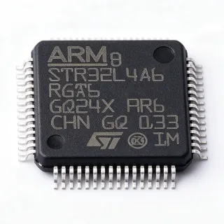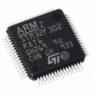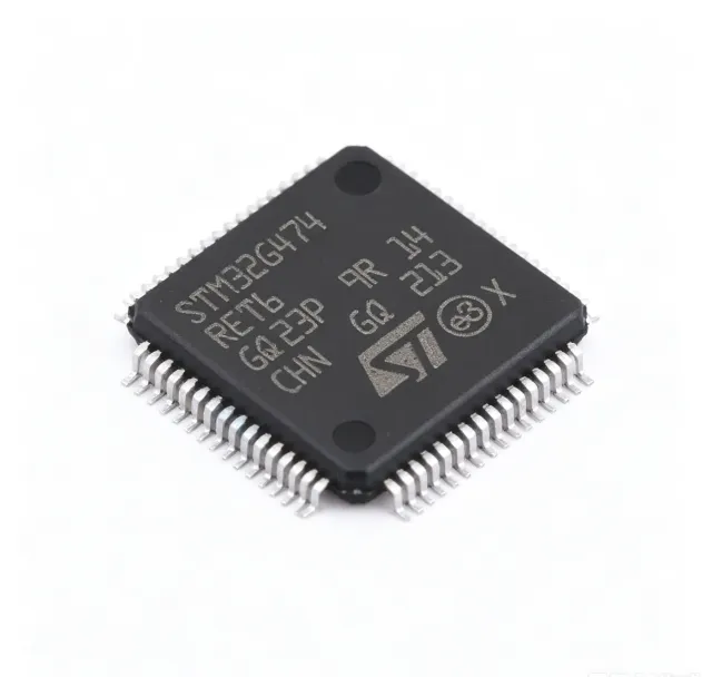
STM32G474RET6 - 170MHz Cortex-M4 MCU 512KB Flash | ST
MPN: STM32G474RET6 ✓ Active| Qty | Unit Price | Extended |
|---|---|---|
| 1 | $9.67 | $9.67 |
| 10 | $8.9 | $89.00 |
| 100 | $8.15 | $815.00 |
| 500 | $7.5 | $3,750.00 |
| 1,000 | $6.95 | $6,950.00 |
STM32G474RET6 Overview
A microcontroller (MCU) is a compact integrated circuit that governs a specific operation in an embedded system, integrating a processor core, memory, and programmable peripherals on a single chip. The STM32G474RET6 belongs to the STM32G4 mainstream MCU family, which sits between general-purpose MCUs and digital signal processors within the embedded-processor hierarchy, and is purpose-built for mixed-signal real-time control.
Key features include the Arm Cortex-M4 core with single-precision FPU and DSP instructions delivering 213 DMIPS, 512 KB flash with ART accelerator, and a rich analog set: a 12-bit ADC with hardware oversampling, 12-bit DAC channels, high-speed comparators, operational amplifiers, and a high-resolution timer (HRTIM) with 184 ps PWM resolution. Communication interfaces cover SPI, I2C, USART, CAN FD, and USB.
Architecturally, the device pairs the Cortex-M4 with CORDIC and FMAC (filter math) hardware accelerators, offloading trigonometric and filter computations from the CPU so deterministic control loops execute faster. The ART accelerator enables 0-wait-state flash execution at full speed, while low-power modes down to microamp levels support energy-conscious designs operating from a 1.71V to 3.6V supply.
Typical applications include field-oriented control (FOC) of brushless DC motors, digital power conversion (buck, boost, flyback), solar inverters, and industrial automation, where the combination of 5 MSPS-class ADC sampling, on-chip comparators, and HRTIM precision timing is decisive.
Design consideration: keep HRTIM output traces short and away from analog routing, and decouple each VDD/VDDA pin with 100 nF ceramics to preserve ADC accuracy.
This page synthesizes distributor pricing, drop-in alternatives, and practical design notes not found in the STMicroelectronics datasheet.
Drop-in alternatives for STM32G474RET6 — same package, pin-to-pin compatible. Different-package parts requiring PCB rework are excluded.
Variants in this series
Same-series models that are drop-in compatible with STM32G474RET6 (same form factor and footprint) — differing in Communication Interfaces, Core, Flash Memory, Package, SRAM.
Quick Comparison Tool — Select alternative parts for side-by-side comparison:
STM32G473RET6
✅ Drop-In✓ In Stock
$5.44 / Unit
View Datasheet →STM32G484RET6
✅ Drop-In✓ In Stock
$5.44 / Unit
View Datasheet →STM32G4A1RET6
✅ Drop-In ⚠️ 参数待验证✓ In Stock
$5.44 / Unit
View Datasheet →STM32G473RCT6
✅ Drop-In✓ In Stock
$5.44 / Unit
View Datasheet →STM32G474RET3
✅ Drop-In📋 Reference alternative (not in catalog)
STM32G474RET6U
✅ Drop-In📋 Reference alternative (not in catalog)
GD32G553RET6
✅ Drop-In📋 Reference alternative (not in catalog)
STM32G474RET6 Maximum Ratings & Electrical Characteristics
| Core | Arm Cortex-M4F 32-bit with FPU and DSP |
| Maximum Clock Frequency | 170 MHz |
| Performance | 213 DMIPS |
| Flash Memory | 512 KB |
| SRAM | 128 KB |
| Supply Voltage Range | 1.71 V to 3.6 V |
| ADC Resolution | 12-bit |
| DAC Resolution | 12-bit |
| HRTIM PWM Resolution | 184 ps |
| Communication Interfaces | SPI, I2C, USART, CAN FD, USB |
| Hardware Accelerators | CORDIC, FMAC (filter math accelerator) |
| Operating Temperature | -40C to +85C (T6 grade, per suffix coding) |
| Package | LQFP-64 (10x10 mm) |
| Mounting Type | Surface Mount |
| Series | STM32G4 (STM32G474xE line) |
| RoHS Status | Compliant |
STM32G474RET6 Pin Configuration
| Pin 1 | VBAT — Battery backup supply |
| Pin 2 | PC13 — GPIO / backup domain I/O |
| Pin 3 | PC14 — GPIO / OSC32_IN |
| Pin 4 | PC15 — GPIO / OSC32_OUT |
| Pin 5 | PH0/OSC_IN — GPIO / main oscillator input |
| Pin 6 | PH1/OSC_OUT — GPIO / main oscillator output |
| Pin 7 | NRST — System reset (active low) |
| Pin 8 | PC0 — GPIO / ADC input |
| Pin 9 | PC1 — GPIO / ADC input |
| Pin 10 | PC2 — GPIO / ADC input |
| Pin 11 | PC3 — GPIO / ADC input |
| Pin 12 | VSSA — Analog ground |
| Pin 13 | VREF- — ADC reference negative |
| Pin 14 | VREF+ — ADC reference positive |
| Pin 15 | VDDA — Analog supply |
| Pin 16 | PA0 — GPIO / ADC / comparator input |
| Pin 17 | PA1 — GPIO / ADC / comparator input |
| Pin 18 | PA2 — GPIO / USART2_TX / ADC |
| Pin 19 | PA3 — GPIO / USART2_RX / ADC |
| Pin 20 | VSS — Digital ground |
| Pin 21 | VDD — Digital supply |
| Pin 22 | PA4 — GPIO / DAC / ADC |
| Pin 23 | PA5 — GPIO / DAC / ADC |
| Pin 24 | PA6 — GPIO / ADC / SPI1 |
| Pin 25 | PA7 — GPIO / ADC / SPI1 |
| Pin 26 | PC4 — GPIO / ADC input |
| Pin 27 | PC5 — GPIO / ADC input |
| Pin 28 | PB0 — GPIO / ADC / comparator input |
| Pin 29 | PB1 — GPIO / ADC / comparator input |
| Pin 30 | PB2 — GPIO |
| Pin 31 | PB10 — GPIO / I2C / USART |
| Pin 32 | PB11 — GPIO / I2C / USART |
| Pin 33 | VSS — Digital ground |
| Pin 34 | VDD — Digital supply |
| Pin 35 | PB12 — GPIO / SPI2 / comparator |
| Pin 36 | PB13 — GPIO / SPI2 / HRTIM |
| Pin 37 | PB14 — GPIO / SPI2 / HRTIM |
| Pin 38 | PB15 — GPIO / SPI2 / HRTIM |
| Pin 39 | PC6 — GPIO / HRTIM / TIM |
| Pin 40 | PC7 — GPIO / HRTIM / TIM |
| Pin 41 | PC8 — GPIO / HRTIM / TIM |
| Pin 42 | PC9 — GPIO / HRTIM / TIM |
| Pin 43 | PA8 — GPIO / TIM / USART |
| Pin 44 | PA9 — GPIO / TIM / USART |
| Pin 45 | PA10 — GPIO / TIM / USART |
| Pin 46 | PA11 — GPIO / USB DM / TIM |
| Pin 47 | PA12 — GPIO / USB DP / TIM |
| Pin 48 | PA13 — GPIO / SWDIO (debug) |
| Pin 49 | VDDUSB — USB regulator supply |
| Pin 50 | VSS — Digital ground |
| Pin 51 | PA14 — GPIO / SWCLK (debug) |
| Pin 52 | PA15 — GPIO / SPI1 / TIM |
| Pin 53 | PC10 — GPIO / USART / SPI |
| Pin 54 | PC11 — GPIO / USART / SPI |
| Pin 55 | PC12 — GPIO / USART / SPI |
| Pin 56 | PD2 — GPIO / TIM / USART |
| Pin 57 | PB3 — GPIO / SPI1 / TIM |
| Pin 58 | PB4 — GPIO / SPI1 / TIM |
| Pin 59 | PB5 — GPIO / SPI1 / I2C |
| Pin 60 | PB6 — GPIO / I2C1 / USART |
| Pin 61 | PB7 — GPIO / I2C1 / USART |
| Pin 62 | PB8 — GPIO / I2C1 / TIM |
| Pin 63 | PB9 — GPIO / I2C1 / TIM |
| Pin 64 | VSS — Digital ground |
Typical Applications
STM32G474RET6 is suitable for 6 applications: Brushless Motor Control (FOC), Digital Power Conversion, Solar Inverters, Industrial Automation & PLC I/O, Battery-Powered Portable Instruments, Chargers & Wireless Power Transmitters.
Brushless Motor Control (FOC)
The STM32G474RET6 is engineered for field-oriented control of BLDC and PMSM motors. Its 170 MHz Cortex-M4F executes FOC current loops with the FPU, while the CORDIC accelerator computes sine/cosine transformations in hardware, cutting loop latency. The HRTIM generates complementary PWM with 184 ps resolution and programmable dead-time, critical for efficient three-phase bridges. On-chip op-amps amplify shunt currents and comparators provide cycle-by-cycle overcurrent protection without external parts. ST's motor-control SDK on this MCU delivers sensorless and encoder-based reference implementations for industrial drives.
Recommended
Digital Power Conversion
Digital power supplies - LLC, totem-pole PFC, buck and flyback converters - rely on the STM32G474RET6's high-resolution timer and fast analog peripherals. The HRTIM's 184 ps PWM resolution enables duty-cycle and phase-shift precision unattainable with standard timers, while 12-bit ADC sampling synchronized to PWM trigger points captures current and voltage waveforms with minimal latency. The B-G474E-DPOW1 Discovery kit from ST demonstrates digital power designs on exactly this MCU. Fast comparator-based protection reacts within microseconds, safeguarding power stages during faults, and FMAC filtering smooths control-loop feedback.
Recommended
Solar Inverters
Solar string and micro inverters demand simultaneous MPPT control, grid-synchronized current shaping, and safety compliance - all tasks the STM32G474RET6 handles on one chip. The 12-bit ADC with hardware oversampling samples PV voltage/current and grid waveforms; the HRTIM drives interleaved boost and inverter stages with sub-nanosecond PWM granularity; and CORDIC accelerates the sine-modulation math for grid injection. CAN FD connectivity supports plant-level monitoring, while multiple low-power modes keep housekeeping consumption low during night standby operation of the inverter system.
Recommended
Industrial Automation & PLC I/O
In industrial automation nodes, the STM32G474RET6 provides robust connectivity and analog acquisition. Its CAN FD interface achieves up to 5 Mbit/s for deterministic fieldbus communication, while multiple USARTs and SPIs connect to sensors, encoders, and HMI modules. The rich 12-bit ADC array with oversampling handles analog process variables (0/4-20 mA loops via external conditioning), and hardware comparators implement fast threshold alarms independently of software. Operation from 1.71 V to 3.6 V with industrial temperature tolerance and an extensive peripheral mix makes it a compact single-chip controller for modular PLC I/O cards.
Recommended
Battery-Powered Portable Instruments
Portable measurement and diagnostic instruments benefit from the STM32G474RET6's balance of compute and efficiency. Running from a 1.71 V rail, it tolerates Li-ion battery discharge windows directly through a small LDO. Low-power modes reduce consumption to microamp levels between measurements, with wake-up over USART, I2C or external lines. The 12-bit ADC with hardware oversampling improves effective resolution for sensor readings without external delta-sigma converters, and 512 KB flash stores rich measurement firmware, logging tables, and USB device stacks for PC connectivity in a single 10x10 mm LQFP device.
Recommended
Chargers & Wireless Power Transmitters
Fast chargers and Qi wireless power transmitters use the STM32G474RET6's HRTIM for full-bridge and half-bridge PWM generation with precise phase control, while on-chip op-amps measure current and voltage feedback for constant-current/constant-voltage regulation. CAN FD and USB interfaces support smart-charging protocols (USB-PD stacking via external controllers), and the fast ADC monitors battery temperature and pack voltage. Hardware comparators enable cycle-by-cycle overcurrent protection in the power stage. The 170 MHz core handles protocol negotiation, telemetry, and safety state machines concurrently with the real-time power loop.
Recommended
Recommended Products Summary
Engineering reference data for STM32G474RET6 — comparison, design guidance, and compliance information.
Selection Guide
Comparison with Alternatives
| Parameter | This Product | STM32G473RET6 | STM32G484RET6 | STM32G473RCT6 | STM32G4A1RET6 | GD32G553RET6 |
|---|---|---|---|---|---|---|
| Package | LQFP-64 (10x10) | LQFP-64 - same | LQFP-64 - same | LQFP-64 - same | LQFP-64 - same | LQFP-64 - same |
| Brand | STMicroelectronics | STMicroelectronics | STMicroelectronics | STMicroelectronics | STMicroelectronics | GigaDevice |
| CAN FD | Yes | Yes | Yes | Yes | Yes | Yes (per GD32G5 series) |
Key Differentiators
- Full HRTIM and complete advanced analog set (vs STM32G473RET6)
- Extended +105C temperature operation (vs STM32G474RET3)
- Guaranteed firmware compatibility over cross-brand (vs GD32G553RET6)
Design Notes
Decouple every VDD pin with 100 nF ceramic capacitors placed within 2 mm of the pin, plus one bulk 4.7 uF capacitor near the device. VDDA must be filtered separately (ferrite bead + 1 uF + 10 nF) to preserve the 12-bit ADC accuracy; VREF+ should be driven from a low-noise reference or clean 3.3 V if the full ADC accuracy is required. The internal USB regulator supply pin (VDDUSB) requires its own decoupling per ST layout guidelines.
HRTIM outputs (up to 184 ps resolution) drive power-stage gates; route them as matched-length pairs with ground return vias nearby to limit ringing and crosstalk into analog traces. Keep ADC input routing away from HRTIM and USB lines. The datasheet package chapter and ST application notes AN4435/AN4748 give G4-family layout recommendations; place SWDIO/SWCLK pads accessible for debugging even in production layouts.
When migrating between the STM32G473/G474/G484 drop-in alternatives, do not assume peripheral equality: the G473 omits some G474 analog features, and firmware compiled for G474 may reference peripherals absent on the cheaper line. Also verify temperature-grade suffixes (T3 vs T6) match the end-product environment, and enable the flash read protection (RDP) options deliberately - incorrect option-byte programming can permanently lock the device.
Compliance Information
RoHS compliance per distributor listings (DigiKey/LCSC). REACH, halogen-free and conflict-minerals status not stated in provided data - verify on the ST product page.