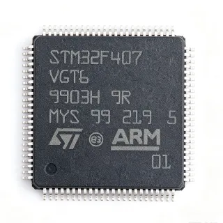
STM32G474VET6 - 170MHz Arm Cortex-M4F MCU | STMicroelectronics
MPN: STM32G474VET6 ✓ Active| Qty | Unit Price | Extended |
|---|---|---|
| 1 | $8.5 | $8.50 |
| 10 | $7.65 | $76.50 |
| 100 | $6.8 | $680.00 |
| 500 | $6.12 | $3,060.00 |
| 1,000 | $5.44 | $5,440.00 |
STM32G474VET6 Overview
What is a microcontroller? A microcontroller (MCU) is a compact integrated circuit containing a processor core, memory, and programmable input/output peripherals on a single chip. It is the brain of embedded systems, executing firmware to control everything from simple LED blinkers to complex motor drives. In the hierarchy of computing devices, a microcontroller falls under embedded processors, which are specialized for real-time control tasks, as opposed to general-purpose CPUs found in personal computers. The STM32G474VET6 exemplifies a modern MCU with its high clock speed, rich analog integration, and advanced timer capabilities.
Key features of the STM32G474VET6 include 512 KB of flash memory and 128 KB of SRAM, providing ample space for complex control algorithms. It supports a wide supply voltage range of 1.71V to 3.6V, ensuring compatibility with various power rails. The device includes a comprehensive set of communication interfaces: I2C, SPI, USART, CAN FD, and USB, enabling seamless connectivity in industrial networks. Additionally, it features a 12-bit DAC, multiple 12-bit ADCs with up to 5 MSPS, and a high-resolution timer (HRTIM) capable of generating PWM signals with sub-nanosecond precision, crucial for digital power supplies.
The STM32G474VET6 is built on ST's advanced 90nm process technology, balancing performance and power efficiency. The Cortex-M4 core with FPU accelerates mathematical computations, essential for real-time control algorithms like FOC (Field-Oriented Control) for motors. The device also includes a Memory Protection Unit (MPU) and a cryptographic acceleration unit, enhancing security for connected applications. Its rich peripheral set and high-speed timers make it a preferred choice for engineers designing high-performance control systems.
Typical applications include field-oriented control of brushless DC motors, digital power conversion (e.g., LLC resonant converters), solar inverters, and industrial automation. The high-resolution timer and fast ADC enable precise current and voltage sensing, critical for closed-loop control. In motor control, the STM32G474VET6 can generate six-step PWM signals with dead-time insertion, reducing external component count.
When designing with this MCU, ensure proper decoupling of the power supply pins with 100nF capacitors placed close to each VDD pin. The VDDA pin should be filtered with a ferrite bead and a 1uF capacitor to minimize analog noise. Also, consider the thermal performance: the LQFP100 package has a thermal resistance of 46°C/W, so adequate PCB copper area is recommended for high-current applications.
Drop-in alternatives for STM32G474VET6 — same package, pin-to-pin compatible. Different-package parts requiring PCB rework are excluded.
Variants in this series
Same-series models that are drop-in compatible with STM32G474VET6 (same form factor and footprint) — differing in High-Resolution Timer, Package.
Quick Comparison Tool — Select alternative parts for side-by-side comparison:
STM32G473VET6
✅ Drop-In ⚠️ Specs Unverified📋 Reference alternative (not in catalog)
STM32G474VET6
✅ Drop-In✓ In Stock
$5.44 / Unit
View Datasheet →STM32G474VET6
✅ Drop-In✓ In Stock
$5.44 / Unit
View Datasheet →STM32G474VET6
✅ Drop-In✓ In Stock
$5.44 / Unit
View Datasheet →STM32G474VET6 Maximum Ratings & Electrical Characteristics
| Core | Arm Cortex-M4 with FPU |
| Maximum Clock Frequency | 170 MHz |
| Flash Memory | 512 KB |
| SRAM | 128 KB |
| Supply Voltage Range | 1.71 V to 3.6 V |
| Package | LQFP-100 (14x14 mm) |
| GPIO Pins | 86 |
| ADC Resolution | 12-bit |
| ADC Sample Rate | 5 MSPS |
| DAC Resolution | 12-bit |
| Communication Interfaces | I2C, SPI, USART, CAN FD, USB |
| High-Resolution Timer | Yes (HRTIM) |
| Operating Temperature Range | -40C to +85C |
| RoHS Status | Compliant |
| Mounting Type | Surface Mount |
STM32G474VET6 Pin Configuration
| Pin 1 | VBAT — Battery backup supply |
| Pin 2 | PC13 — GPIO / RTC output |
| Pin 3 | PC14 — GPIO / OSC32_IN |
| Pin 4 | PC15 — GPIO / OSC32_OUT |
| Pin 5 | PF0 — GPIO |
| Pin 6 | PF1 — GPIO |
| Pin 7 | NRST — Reset (active low) |
| Pin 8 | VDD — Digital power supply |
| Pin 9 | VSS — Digital ground |
| Pin 10 | VDDA — Analog power supply |
| Pin 11 | VREF+ — ADC reference voltage |
| Pin 12 | VREF- — ADC reference ground |
| Pin 13 | PA0 — GPIO / ADC input |
| Pin 14 | PA1 — GPIO / ADC input |
| Pin 15 | PA2 — GPIO / USART2_TX |
| Pin 16 | PA3 — GPIO / USART2_RX |
| Pin 17 | PA4 — GPIO / DAC_OUT1 |
| Pin 18 | PA5 — GPIO / DAC_OUT2 |
| Pin 19 | PA6 — GPIO / TIM1_CH1 |
| Pin 20 | PA7 — GPIO / TIM1_CH2 |
Typical Applications
STM32G474VET6 is suitable for 6 applications: Field-Oriented Control of BLDC Motors, Digital Power Conversion (LLC Resonant Converter), Solar Inverter, Industrial Automation (PLC), Medical Device (Patient Monitoring), Robotics (Servo Control).
Field-Oriented Control of BLDC Motors
The STM32G474VET6 is ideal for FOC of brushless DC motors. Its high-resolution timer (HRTIM) generates precise PWM signals with dead-time insertion, while the fast ADC (5 MSPS) samples phase currents for closed-loop control. The Cortex-M4 FPU accelerates the Clarke and Park transforms, enabling efficient real-time torque and speed control. In a typical setup, the MCU reads current sensors via the ADC, computes the rotor position using an encoder or Hall sensors, and outputs six-step PWM to the inverter bridge. The HRTIM's sub-nanosecond resolution ensures minimal torque ripple and high efficiency. Compared to older MCUs, the G474's integrated analog peripherals reduce external component count, lowering BOM cost and board space. Designers must ensure proper decoupling of the ADC reference voltage to maintain measurement accuracy.
Recommended
Digital Power Conversion (LLC Resonant Converter)
The STM32G474VET6 excels in digital power conversion, particularly LLC resonant converters. Its HRTIM can generate PWM frequencies up to 1 GHz with sub-nanosecond duty cycle resolution, essential for precise control of the resonant tank. The fast ADC monitors output voltage and current, enabling closed-loop regulation with high bandwidth. The MCU's comparators and DACs can implement protection features like overcurrent and overvoltage detection without external components. In a typical LLC converter, the G474 controls the switching frequency to regulate output voltage, using the ADC to sense the output and the HRTIM to drive the MOSFETs. The integrated analog peripherals simplify the design, reducing component count and improving reliability. Engineers should pay attention to the thermal design, as the LQFP-100 package has a theta_JA of 46°C/W, requiring adequate PCB copper for heat dissipation.
Recommended
Solar Inverter
The STM32G474VET6 is well-suited for solar inverters, where it manages maximum power point tracking (MPPT) and grid synchronization. Its high-speed ADC and timers enable precise measurement of PV panel voltage and current, while the HRTIM generates PWM for the DC-DC boost converter and the DC-AC inverter. The Cortex-M4 FPU accelerates MPPT algorithms like Perturb & Observe, improving energy harvesting efficiency. The MCU's CAN FD interface allows communication with other system components, such as battery management systems. In a typical solar inverter, the G474 reads the PV voltage and current, computes the optimal operating point, and adjusts the PWM duty cycle accordingly. The integrated comparators can detect overcurrent conditions and shut down the system within microseconds. Designers must ensure proper isolation between the high-voltage side and the MCU, using optocouplers or digital isolators.
Recommended
Industrial Automation (PLC)
The STM32G474VET6 is a robust choice for programmable logic controllers (PLCs) in industrial automation. Its rich set of communication interfaces (CAN FD, USART, SPI, I2C) enables seamless integration with fieldbus networks like CANopen and Modbus. The MCU's high-speed ADC and comparators can handle analog input modules, while its timers generate precise PWM for actuator control. The 512 KB flash and 128 KB SRAM provide ample space for complex control logic and data logging. In a typical PLC, the G474 scans digital inputs, executes the user program, and updates outputs within a deterministic cycle time. The Cortex-M4 FPU accelerates floating-point calculations, useful for PID loops. The wide operating temperature range (-40°C to +85°C) ensures reliability in harsh industrial environments. Designers should implement a watchdog timer and brown-out detection to enhance system robustness.
Recommended
Medical Device (Patient Monitoring)
The STM32G474VET6 can be used in medical devices like patient monitors, where it processes biosignals such as ECG and SpO2. Its high-resolution ADC (12-bit, 5 MSPS) captures analog signals with high fidelity, while the Cortex-M4 FPU handles digital filtering and signal processing algorithms. The MCU's low power consumption and wide supply voltage range (1.71V to 3.6V) support battery-powered operation. In a typical patient monitor, the G474 samples the ECG signal via the ADC, applies a bandpass filter to remove noise, and computes heart rate. The integrated DAC can generate alarm tones, and the communication interfaces (USB, UART) transmit data to a display or central station. The MCU's security features, including a memory protection unit, help protect patient data. Designers must ensure compliance with medical standards like IEC 60601, which may require additional isolation and safety measures.
Recommended
Robotics (Servo Control)
The STM32G474VET6 is ideal for robotics applications, particularly servo control. Its high-resolution timer and fast ADC enable precise position and velocity control of servo motors. The Cortex-M4 FPU accelerates inverse kinematics calculations, allowing smooth multi-axis motion. In a typical robotic arm, the G474 reads encoder feedback via the timer's encoder interface, computes the error, and generates PWM signals to drive the servo motors. The integrated comparators can implement torque limiting and emergency stop functions. The MCU's CAN FD interface facilitates communication between multiple joints in a distributed control system. The 512 KB flash allows storing complex motion profiles. Designers should consider using a real-time operating system (RTOS) to manage multiple control loops and communication tasks efficiently.
Recommended
Recommended Products Summary
Engineering reference data for STM32G474VET6 — comparison, design guidance, and compliance information.
Selection Guide
Comparison with Alternatives
| Parameter | This Product | STM32G473VET6 | STM32G474RET6 | STM32G474VET6 |
|---|---|---|---|---|
| Package | LQFP-100 | LQFP-100 | LQFP-64 | LQFP-100 |
| Brand | STMicroelectronics | STMicroelectronics | STMicroelectronics | STMicroelectronics |
| Core | Cortex-M4 with FPU | Cortex-M4 with FPU | Cortex-M4 with FPU | Cortex-M4 with FPU |
| Max Clock Frequency | 170 MHz | 170 MHz | 170 MHz | 170 MHz |
| Flash Memory | 512 KB | 512 KB | 512 KB | 512 KB |
| SRAM | 128 KB | 128 KB | 128 KB | 128 KB |
| ADC Sample Rate | 5 MSPS | 5 MSPS | 5 MSPS | 5 MSPS |
| High-Resolution Timer | Yes | Yes (less advanced) | Yes | Yes |
Key Differentiators
- High-resolution timer (HRTIM) with sub-nanosecond PWM resolution (vs STM32G473VET6)
- Dual 12-bit DACs (vs STM32G473VET6)
- Larger package with more GPIOs (vs STM32G474RET6)
Design Notes
Decouple each VDD pin with a 100nF ceramic capacitor placed as close as possible to the pin. Additionally, place a 4.7uF capacitor on the VDDA pin to filter analog noise. Use a ferrite bead between VDD and VDDA to isolate digital switching noise from the analog supply.
The LQFP-100 package has a thermal resistance (theta_JA) of 46°C/W. For high-current applications, ensure adequate PCB copper area and consider adding thermal vias under the exposed pad (if available) to improve heat dissipation. Monitor junction temperature to stay within the -40°C to +85°C operating range.
For the ADC, use a star-ground topology to minimize noise. Place the VREF+ and VREF- pins with a 1uF capacitor and a 10nF capacitor in parallel. Route analog signals away from high-speed digital traces to reduce crosstalk.
Compliance Information
RoHS compliant per STMicroelectronics product page. Not AEC-Q100 qualified (industrial grade).