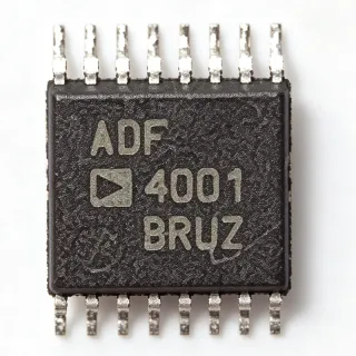
AD5303ARU - Dual 8-Bit Rail-to-Rail DAC | Analog Devices
N.º de pieza: AD5303ARU ✓ ActivoAD5303ARU Descripción general
A DAC is a data-conversion integrated circuit that translates a digital code into a proportional analog voltage or current. The AD5303 belongs to the voltage-output DAC family, where buffered outputs are driven directly by on-chip amplifiers. Its rail-to-rail output stage allows the analog outputs to approach the available supply rails, while the dual-channel architecture supports two independent analog control or excitation channels in a compact footprint.
The principal features include 8-bit resolution on each channel, a versatile 3-wire serial interface compatible with SPI, QSPI, MICROWIRE, and DSP interface standards, and serial clock operation up to 30 MHz. Each converter derives its reference from a dedicated reference pin, allowing the two output voltages to be scaled independently. The single-supply operating range supports both 3.3 V and 5 V systems.
Internally, the device uses a resistor-string DAC architecture followed by buffered output amplifiers. This arrangement provides direct voltage output without requiring an external output buffer and simplifies connection to analog front ends. The 16-lead TSSOP package is suitable for compact analog and mixed-signal designs, while the dual channel count improves utilization when a system needs two matched control signals.
Typical applications include industrial process control, programmable test and measurement equipment, battery-powered instrumentation, sensor excitation, automated test equipment, and general-purpose analog signal generation. Its 230 uA current consumption at 3 V is especially useful in portable and distributed sensing systems where each subsystem must limit standby power.
Designers should treat the reference pins as precision analog nodes, route them away from digital switching currents, and use the pin-description table in the manufacturer datasheet when assigning PCB tracks. Confirm output settling time, reference voltage limits, and logic-level compatibility against the intended clock rate and analog settling requirements.
This page combines manufacturer specifications, drop-in device alternatives, application guidance, and design notes for engineers evaluating the AD5303ARU across low-power analog and mixed-signal systems.
Alternativas directas para AD5303ARU — mismo encapsulado, compatible pin a pin. Se excluyen las piezas de otro encapsulado que requieren retrabajo de la PCB.
AD5303ARUZ
✅ Sustitución directa📋 Alternativa de referencia (no en el catálogo)
AD5303BRU
✅ Sustitución directa📋 Alternativa de referencia (no en el catálogo)
AD5313ARUZ
✅ Sustitución directa ⚠️ Especificaciones sin verificar📋 Alternativa de referencia (no en el catálogo)
AD5313BRU
✅ Sustitución directa ⚠️ Especificaciones sin verificar📋 Alternativa de referencia (no en el catálogo)
AD5323ARUZ
✅ Sustitución directa ⚠️ Especificaciones sin verificar📋 Alternativa de referencia (no en el catálogo)
AD5323BRU
✅ Sustitución directa ⚠️ Especificaciones sin verificar📋 Alternativa de referencia (no en el catálogo)
AD5303ARU Valores máximos y características eléctricas
| Number of DAC Channels | 2 |
| Resolución | 8 bits per channel |
| DAC Architecture | Resistor string with buffered voltage output |
| Supply Voltage Range | 2.5 V to 5.5 V |
| Current Consumption | 230 uA at 3 V |
| Tipo de salida | Buffered voltage output |
| Output Swing | Rail-to-rail |
| Serial Interface | 3-wire serial interface |
| Interface Compatibility | SPI, QSPI, MICROWIRE, and DSP interfaces |
| Maximum Serial Clock Rate | 30 MHz |
| Reference Inputs | 2 independent reference pins |
| Encapsulado | 16-lead TSSOP |
| Tipo de montaje | Surface mount |
Guía de configuración de pines de AD5303ARU 16-lead tssop
Configuración de pines para AD5303ARU (encapsulado 16-lead tssop). Este componente analógico presenta pines de entrada, salida y alimentación. Consulte la hoja de datos del fabricante para conocer las configuraciones de los pines de ajuste de offset, compensación y habilitación. Ideal para circuitos de acondicionamiento de señal y amplificadores.

No hay datos detallados de patillaje disponibles para AD5303ARU.
Consulte la hoja de datos para ver la configuración completa de patillas.
Aplicaciones típicas
AD5303ARU es adecuado para 6 aplicacións: Industrial Process Control, Programmable Test and Measurement, Portable Sensor Excitation, Battery-Powered Data Acquisition, Automated Test Equipment, Audio and Communication Control.
Industrial Process Control
The AD5303ARU fits closed-loop industrial controllers that need two adjustable analog command outputs from a compact controller board. Its two independent 8-bit channels can represent actuator commands, setpoints, or offset adjustments, while the 2.5 V to 5.5 V supply range supports both 24 V industrial designs with local regulation and compact 5 V control electronics. The 30 MHz serial-interface capability provides ample bandwidth for periodic updates from an industrial microcontroller or PLC interface module. Because the outputs use buffered rail-to-rail stages, external unity-gain amplifiers are unnecessary for normal high-impedance loads. Confirm loop settling requirements and analog input ranges before using the 8-bit step size for precision positioning.
Recomendado
Programmable Test and Measurement
The AD5303ARU can generate two independent stimulus levels for automated test equipment, bench instruments, and board-level test fixtures. Its 3-wire serial interface supports SPI, QSPI, MICROWIRE, and DSP standards, while operation up to 30 MHz permits rapid code updates during automated sequences. A dual converter avoids duplicating the digital interface and reference distribution when a fixture requires two bias or excitation voltages. The buffered rail-to-rail outputs can drive high-impedance measurement inputs directly, although cable loading, settling time, and reference accuracy must be evaluated for each channel. The 230 uA consumption at 3 V also supports compact low-power test modules.
Recomendado
Portable Sensor Excitation
The AD5303ARU is useful in portable or distributed sensor modules that must provide adjustable excitation or offset voltages beside a sensing frontend. Its 230 uA current consumption at a 3 V supply leaves more of the system power budget for sensing, signal conditioning, and short-range communications. Two independently referenced outputs can drive separate resistive bridges or compensate two measurement channels without duplicating the converter package. Rail-to-rail buffered operation provides useful output range in low-voltage designs, but the selected reference and load must remain within their documented limits. Validate the 8-bit resolution against the required excitation step, and account for reference drift when long-duration measurements depend on accurate excitation.
Recomendado
Battery-Powered Data Acquisition
The AD5303ARU supports low-power data-acquisition systems that need controllable analog outputs alongside sensors and amplifiers. Its single-supply operation from 2.5 V to 5.5 V allows direct use of a regulated 3.3 V or 5 V rail, and the 230 uA consumption at 3 V limits the converter's contribution to standby demand. Two buffered channels can generate offset, span, or excitation voltages for instrumentation amplifiers and analog-to-digital converters. Because the DAC includes on-chip output amplifiers, the signal path remains compact, but external protection may be needed when outputs drive long cables or potentially mistuned loads. Confirm output stability, reference settling, and sleep-state behavior in the complete analog subsystem.
Recomendado
Automated Test Equipment
The AD5303ARU is appropriate for automated test equipment that commands two analog levels through a common digital bus. Its SPI-compatible 3-wire interface and clock rate up to 30 MHz allow the converter to be updated rapidly between test steps without requiring separate data buses for each channel. Rail-to-rail buffered outputs support common low-voltage fixture biases and signal conditioning inputs, while the dual-reference arrangement allows independent scaling of the two commands. The 16-lead TSSOP package conserves board area in densely populated test-interface cards. When accuracy is critical, characterize the reference at temperature, verify full-scale settling after a code change, and keep high-current switching nodes away from the reference and analog output traces.
Recomendado
Audio and Communication Control
The AD5303ARU can provide two low-level control or bias voltages in audio and communication equipment where a dedicated audio codec is unnecessary. The buffered rail-to-rail outputs may set mixer-control levels, line-driver references, or small signal offsets, and the fast 3-wire interface allows a host controller to update both channels during configuration. Its 230 uA consumption at 3 V suits compact peripheral modules, although noise-sensitive analog paths require careful grounding and reference filtering. Because this is an 8-bit converter, use it for coarse control levels rather than fine amplitude synthesis, and evaluate glitch energy when updating codes between sensitive operating states. Keep return currents out of the reference ground path to avoid modulation of the two outputs.
Recomendado
Resumen de productos recomendados
Datos de referencia de ingeniería para AD5303ARU — comparación, orientación de diseño e información de cumplimiento.
Guía de selección
Comparación con alternativas
| Parámetro | Este producto | AD5303ARUZ | AD5303BRU | AD5313ARUZ | AD5313BRU | AD5323ARUZ | AD5323BRU |
|---|---|---|---|---|---|---|---|
| Brand | Analog Devices | Analog Devices | Analog Devices | Analog Devices | Analog Devices | Analog Devices | Analog Devices |
| Package | 16-lead TSSOP | 16-lead TSSOP - same | 16-lead TSSOP - same | 16-lead TSSOP - same | 16-lead TSSOP - same | 16-lead TSSOP - same | 16-lead TSSOP - same |
| Resolution | 8 bits | 8 bits | 8 bits | 10 bits | 10 bits | 12 bits | 12 bits |
| Number of DAC Channels | 2 | 2 | 2 | 2 | 2 | 2 | 2 |
| Supply Voltage Range | 2.5 V to 5.5 V | 2.5 V to 5.5 V | 2.5 V to 5.5 V | 2.5 V to 5.5 V | 2.5 V to 5.5 V | 2.5 V to 5.5 V | 2.5 V to 5.5 V |
| Output Type | Buffered rail-to-rail voltage output | Buffered rail-to-rail voltage output | Buffered rail-to-rail voltage output | Buffered voltage output | Buffered voltage output | Buffered voltage output | Buffered voltage output |
| Serial Interface | 3-wire SPI, QSPI, MICROWIRE, and DSP compatible | 3-wire serial interface | 3-wire serial interface | 3-wire serial interface | 3-wire serial interface | 3-wire serial interface | 3-wire serial interface |
| Maximum Serial Clock Rate | 30 MHz | 30 MHz | 30 MHz | 30 MHz | 30 MHz | 30 MHz | 30 MHz |
| Reference Architecture | One reference pin per DAC channel | One reference pin per DAC channel | One reference pin per DAC channel | One reference pin per DAC channel | One reference pin per DAC channel | One reference pin per DAC channel | One reference pin per DAC channel |
Diferenciadores clave
- Lower output resolution than the higher-resolution family alternatives (frente a AD5323ARUZ)
- Dual buffered outputs without external output amplifiers (frente a AD5313ARUZ)
- Directly compatible with SPI-style host interfaces (frente a AD5303BRU)
Notas de diseño
Treat both reference pins as sensitive analog nodes. Route each reference directly to its assigned pin, keep the traces short, and avoid routing them beneath digital clock or serial-data lines. If a reference source sits far from the converter, place the required bypass capacitor at the device rather than at the source. This prevents supply and reference transients from appearing simultaneously on both analog outputs.
Use a compact analog and digital floor-plan with the converter near the interface controller, while keeping analog outputs and reference routing away from switching nodes. The TSSOP package allows the analog pins to be grouped, but pin assignments must be taken from the manufacturer pin-description table. Provide a quiet return path and avoid connecting output return current through the reference ground region.
Do not assume that identical package dimensions guarantee identical behavior when moving from the 8-bit AD5303 to a 10-bit AD5313 or 12-bit AD5323. Confirm serial-register behavior, code scaling, output settling, and reference requirements after substitution. Similarly, confirm the ordering grade and temperature range of AD5303BRU before using it as a production replacement for AD5303ARU.
The 230 uA specification applies to the converter at a 3 V supply. Total analog-channel power depends on the reference source, load current, and whether either output is disabled or updated continuously. Decouple the single supply close to the device and verify startup behavior at the minimum 2.5 V operating voltage, especially when the output load pulls downward during code transitions.
Información de cumplimiento
The manufacturer product page confirms RoHS-relevant product information availability, but no explicit compliance statement was extracted. The component is an analog data converter rather than an automotive-qualified device.