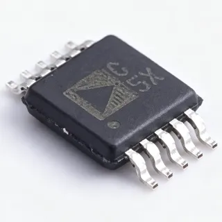
AD976ABRZ - 16-Bit 200 kSPS ADC | Analog Devices
N.º de pieza: AD976ABRZ ✓ ActivoAD976ABRZ Descripción general
An ADC is an interface IC that converts a continuously varying analog voltage into a numeric code for processing by a microcontroller, DSP, FPGA, or industrial controller. The AD976A belongs to the high-speed ADC category and uses a switched-capacitor, successive-approximation architecture. Its parallel data interface makes it suitable for systems that sample rapidly and require direct acquisition-data access without a serial-interface converter.
The converter provides 16-bit resolution, 200 kSPS throughput, single 5 V operation, and an input range of ±10 V. Its internal 2.5 V reference and choice of internal or external reference support flexible board-level signal-chain designs. Maximum power dissipation is listed as 100 mW, making the device suitable for compact industrial, instrumentation, communications, and embedded control systems.
At the heart of the AD976A is a switched-capacitor successive-approximation conversion stage with a parallel output interface. Successive-approximation ADCs generally provide a practical balance among resolution, conversion throughput, power consumption, and implementation complexity. The 16-bit code represents the analog input with a quantization step determined by the selected input range and reference voltage.
Typical uses include industrial process monitoring, instrumentation, communications equipment, data-acquisition systems, and embedded control platforms. The 200 kSPS rate is suitable for sampling waveforms and transducers whose useful bandwidth is well below the converter's Nyquist limit. System designers should also account for acquisition time, input settling, source impedance, reference stability, digital-interface timing, and analog filtering when defining overall measurement accuracy.
For PCB implementation, use the manufacturer's pin-description table to assign the 28 SOIC connections, connect bypass capacitors close to the supply and reference pins, and keep the analog input route away from high-current digital and clock-return paths. The wide-body SOIC package offers more routing space than a narrow-body variant, but careful grounding and decoupling remain necessary to preserve the converter's full 16-bit performance.
This product record combines the manufacturer's converter specifications, package information, sourcing guidance, application context, and engineering notes in one place. It also distinguishes confirmed device characteristics from parameters that require consultation of the AD976 datasheet, helping engineers plan acquisition boards, compare interfaces, and qualify replacements without relying on incomplete distributor summaries.
Alternativas directas para AD976ABRZ — mismo encapsulado, compatible pin a pin. Se excluyen las piezas de otro encapsulado que requieren retrabajo de la PCB.
Variantes de esta serie
Modelos de la misma serie compatibles directamente con AD976ABRZ (mismo factor de forma y huella) — difiere en Architecture, Input Range, Supply Voltage, Resolution, Operating Temperature.
No hay alternativas directas disponibles para este producto.
Solicitar alternativasAD976ABRZ Valores máximos y características eléctricas
| Converter Type | Successive-approximation ADC |
| Resolución | 16 bit |
| Throughput Rate | 200 kSPS |
| Input Channels | 1 input |
| Tensión de alimentación | 5 V |
| Analog Input Range | ±10 V |
| Internal Reference Voltage | 2.5 V |
| Reference Selection | Internal or external |
| Maximum Power Dissipation | 100 mW |
| Linearity Error | 0.0031% |
| Sample Rate | 0.2 MHz |
| Process Technology | BiCMOS |
| Tipo de interfaz | Parallel |
| Encapsulado | 28-pin SOIC, wide body |
| Número de pines | 28 pins |
| Lead Form | Gull wing |
| Package Shape | Rectangular |
| Package Code | SOP |
| Temperature Grade | Industrial |
| Rango de temperatura de funcionamiento | -40 °C to 85 °C |
Guía de configuración de pines de AD976ABRZ sop
Configuración de pines para AD976ABRZ (encapsulado sop). Este componente analógico presenta pines de entrada, salida y alimentación. Consulte la hoja de datos del fabricante para conocer las configuraciones de los pines de ajuste de offset, compensación y habilitación. Ideal para circuitos de acondicionamiento de señal y amplificadores.

No hay datos detallados de patillaje disponibles para AD976ABRZ.
Consulte la hoja de datos para ver la configuración completa de patillas.
Aplicaciones típicas
AD976ABRZ es adecuado para 6 aplicacións: Industrial Process Monitoring, Laboratory Instrumentation, Communications Signal Acquisition, Data Acquisition Systems, Embedded Control and Measurement, Audio and Vibration Analysis.
Industrial Process Monitoring
The AD976ABRZ fits process-monitoring and instrumentation systems that need 16-bit measurement resolution at a moderate sampling rate. Its 200 kSPS throughput provides a practical conversion rate for pressure, temperature, level, and position transducer signals, while the ±10 V input range supports appropriately conditioned industrial sensor outputs. The 5 V supply and parallel interface simplify implementation around a DSP, FPGA, or embedded controller. Designers should place input filtering and settling components close to the converter, reference the analog ground carefully, and verify acquisition timing for the selected sensor bandwidth. The converter's industrial temperature range of -40 °C to 85 °C supports equipment deployed across ordinary factory environments.
Recomendado
Laboratory Instrumentation
The AD976ABRZ can serve as the conversion stage in laboratory measurement equipment requiring more precision than a typical 12-bit mixed-signal converter. Its 16-bit code width supports measurement systems dealing with low-level or closely spaced signal values, and the 200 kSPS rate suits many bandwidth-limited laboratory waveforms. The ±10 V input range allows a practical interface to external signal conditioning, while the internal 2.5 V reference can simplify standalone designs. For precision results, the complete acquisition path must account for sensor noise, analog-filter settling, reference stability, grounding, and calibration. Timing from conversion start to valid parallel data should be coordinated with the controlling processor.
Recomendado
Communications Signal Acquisition
The AD976ABRZ is appropriate for communications equipment that samples conditioned analog waveforms and transfers 16-bit samples to a high-speed digital processing section. Its 200 kSPS throughput can support baseband measurement, envelope observation, modulation analysis, and other signals whose useful bandwidth remains below the converter's sampling limit. The parallel interface allows acquisition data to be captured directly by suitable logic or DSP hardware, avoiding an external serial conversion stage. Signal-chain design must include anti-alias filtering, gain control, source-impedance limits, and sufficient acquisition settling time. Clock and data routing also require controlled digital return paths so converter activity does not degrade the accuracy of the analog input.
Recomendado
Data Acquisition Systems
The AD976ABRZ fits standalone or embedded data-acquisition systems requiring a compact 16-bit converter with direct parallel data access. A 28-pin SOIC can simplify assembly in a mixed analog-and-digital board while offering enough routing flexibility for input conditioning, reference bypass, and interface logic. Its single 5 V supply is useful for systems already operating around standard logic levels, and the 200 kSPS rate supports many general-purpose measurement channels. To preserve the converter's resolution, designers should use a stable reference arrangement, low-noise supply decoupling, a symmetrical analog-ground strategy, and an input driver that settles within the acquisition window. The controller should also capture and timestamp valid conversion results correctly.
Recomendado
Embedded Control and Measurement
The AD976ABRZ can be paired with an embedded processor or FPGA to create a precision control loop that reads analog process variables. Its 16-bit resolution offers more usable measurement granularity than a lower-resolution converter, while 200 kSPS throughput is ample for many motor, actuator, and feedback signals with controlled bandwidth. The parallel interface permits the acquisition result to enter digital control logic directly, although the controller must support the required data width and timing. For closed-loop stability, evaluate conversion latency and acquisition time together with the control update period. Analog filtering, reference quality, grounding, and component tolerances must be included in the loop's overall error budget.
Recomendado
Audio and Vibration Analysis
The AD976ABRZ is suitable for compact analysis platforms that digitize appropriately band-limited audio, vibration, or motion signals and require a 16-bit conversion code. The 200 kSPS sampling rate is suitable for signals whose relevant bandwidth is safely below 100 kHz, with the exact usable bandwidth determined by the anti-alias filter and acquisition behavior. Its parallel output can feed an FPGA or DSP that performs filtering, spectral analysis, or event detection. Designers should pay particular attention to input-driver settling, clock jitter, reference noise, and analog grounding because these factors can affect low-level analysis results. A 5 V supply arrangement also helps simplify integration with mixed-signal processing platforms.
Recomendado
Datos de referencia de ingeniería para AD976ABRZ — comparación, orientación de diseño e información de cumplimiento.
Guía de selección
Comparación con alternativas
| Parámetro | Este producto |
|---|---|
| Package | 28-pin wide-body SOIC |
| Brand | Analog Devices |
| Resolution | 16 bit |
| Throughput Rate | 200 kSPS |
| Input Channels | 1 input |
| Supply Voltage | 5 V |
| Analog Input Range | ±10 V |
| Reference | Internal 2.5 V or external |
| Interface | Parallel |
| Maximum Power Dissipation | 100 mW |
Diferenciadores clave
- Higher conversion throughput than the original AD976 family member (frente a AD976)
- Direct 16-bit parallel acquisition interface (frente a AD976)
- Single-supply operation with a broad analog input range (frente a AD976)
Notas de diseño
Route the analog input as a short, guarded trace directly from the conditioning network to the converter input. Keep the input driver close enough to settle within the acquisition interval specified by the Analog Devices datasheet. Place reference and supply bypass components at their associated pins, connect the exposed analog and digital grounds according to the manufacturer's guidance, and separate the input trace from clock, logic, and switching-current paths to minimize conversion-coupled errors.
The parallel data bus can create fast edge currents even though the converter's average power is low. Route clock and data outputs consistently, provide a continuous return path beneath the bus where practical, and avoid splitting the analog and digital ground regions without following the recommended star or grounding strategy. Confirm that the receiving device can meet setup and hold timing from the manufacturer timing table, and avoid adding unnecessary long traces or branch stubs to the parallel interface.
Do not select an analog input range or reference configuration independently of the external resistor network and application schematic. Compute the complete signal gain, check absolute input-pin limits, and verify that the input source settles within the converter's acquisition requirement. Also avoid using a generic 28-pin SOP drawing as a substitute for the official pin table: the AD976 family has analog, digital, reference, clock, and parallel-bus connections whose functions must be assigned from the manufacturer documentation.
Información de cumplimiento
The AD976ABRZ is identified as an industrial-temperature Analog Devices converter. Confirm environmental material declarations and qualification status in the current manufacturer product documentation before assigning compliance requirements.