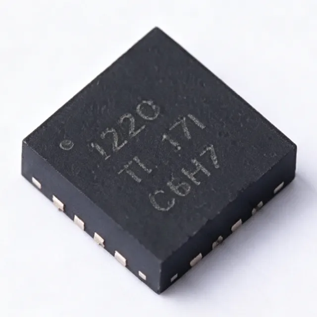
ADS1220IRVAR - 24-Bit 2kSPS Delta-Sigma ADC with PGA | Texas Instruments
N.º de pieza: ADS1220IRVAR ✓ Activo| Cant. | Precio unitario | Total |
|---|---|---|
| 1 | $4.85 | $4,85 |
| 10 | $4.36 | $43,60 |
| 100 | $3.88 | $388,00 |
| 500 | $3.49 | $1.745,00 |
| 1.000 | $3.1 | $3.100,00 |
| 3.000 | $2.65 | $7.950,00 |
ADS1220IRVAR Descripción general
A delta-sigma ADC is a type of analog-to-digital converter that oversamples the input signal far above Nyquist and applies digital filtering to push quantization noise out of band, achieving very high resolution. It is the dominant architecture for precision sensor measurement (ADC -> data converter -> mixed-signal front end -> semiconductor). The ADS1220 sits in TI's precision ADC portfolio alongside the ADS1120 (lower channel count, similar feature set) and the ADS131M family (higher speed, simultaneous-sampling focus).
Key features include a flexible input multiplexer supporting two differential or four single-ended inputs, a low-noise chopper-stabilized PGA with gains of 1, 2, 4, 8, 16, 32, 64, and 128, two matched programmable excitation current sources up to 1.5 mA for ratiometric RTD and thermistor measurements, a burnout current source for open-wire sensor detection, and a 2.048 V integrated reference with 10 ppm/C typical drift. The digital filter provides simultaneous 50 Hz and 60 Hz line-noise rejection at 20 SPS.
Technically, the ADS1220 achieves up to 20 bits effective resolution at the maximum 2 kSPS data rate and up to 29.5 bits noise-free resolution at 20 SPS, using a third-order delta-sigma modulator followed by a configurable SINC digital filter. The SPI interface supports clock speeds up to 4.5 MHz with optional CRC packet checking for robust communication in electrically noisy industrial environments.
Typical applications include RTD and thermocouple temperature measurement, bridge sensor (load cell, strain gauge) signal digitization, battery cell voltage monitoring, and portable instrumentation such as handheld multimeters, where its low quiescent current and high channel integration reduce both system size and energy budget.
Design consideration: for ratiometric RTD designs, route the IDAC excitation current through the reference resistor so reference and ADC share the same supply drift; keep AVDD between 2.3 V and 5.5 V, decouple both AVDD and DVDD with 1 uF X7R ceramics placed within 5 mm of the pins, and ground the exposed thermal pad directly to the analog ground plane.
This page synthesizes distributor pricing, drop-in alternative analysis, and practical design notes not found on the manufacturer datasheet, helping engineers select, source, and qualify the ADS1220IRVAR for production.
Alternativas directas para ADS1220IRVAR — mismo encapsulado, compatible pin a pin. Se excluyen las piezas de otro encapsulado que requieren retrabajo de la PCB.
Variantes de esta serie
Modelos de la misma serie compatibles directamente con ADS1220IRVAR (mismo factor de forma y huella) — difiere en Architecture, Operating Temperature, Package, Resolution.
Herramienta de comparación rápida — seleccione piezas alternativas para compararlas lado a lado:
ADS1220IPWR
✅ Sustitución directa✓ En stock
$1.91 / unidad
Ver hoja de datos →ADS1220IPWR
✅ Sustitución directa✓ En stock
$1.91 / unidad
Ver hoja de datos →ADS1220IRVAT
✅ Sustitución directa📋 Alternativa de referencia (no en el catálogo)
ADS1120IRVAR
✅ Sustitución directa ⚠️ Especificaciones sin verificar📋 Alternativa de referencia (no en el catálogo)
ADS1220IPWR
✅ Sustitución directa✓ En stock
$1.91 / unidad
Ver hoja de datos →ADS1220IRVAR Valores máximos y características eléctricas
| Resolución | 24 bits |
| Architecture | Delta-Sigma (3rd-order modulator) |
| Number of Input Channels | 4 single-ended or 2 differential (via MUX) |
| Maximum Sample Rate | 2 kSPS |
| Input Voltage Range (AVDD) | 2.3 V to 5.5 V |
| Digital I/O Voltage (DVDD) | 1.8 V to 3.6 V |
| Programmable Gain Amplifier Gains | 1, 2, 4, 8, 16, 32, 64, 128 |
| Effective Resolution (max) | 20 bits at 2 kSPS, up to 29.5 bits NFR at 20 SPS |
| Integrated Reference Voltage | 2.048 V (10 ppm/C typical drift) |
| IDAC Excitation Current | 10 uA to 1.5 mA, 2 matched sources |
| Communication Interface | SPI-compatible (up to 4.5 MHz) |
| Burnout Current Source | Yes (open-wire sensor detection) |
| 50/60 Hz Rejection | Yes, simultaneous at 20 SPS |
| Encapsulado | VQFN-16 (RVA) 3.5 mm x 3.5 mm with EP |
| Tipo de montaje | Surface Mount |
| Temperatura de funcionamiento | -40 C to +125 C |
| Nivel MSL | 2 (1 year) |
| Estado RoHS | Compliant |
Configuración de pines de ADS1220IRVAR
| Pin 1 | DRDY — Data ready output (active low) |
| Pin 2 | DOUT — SPI data output |
| Pin 3 | DIN — SPI data input |
| Pin 4 | SCLK — SPI serial clock |
| Pin 5 | CS — SPI chip select (active low) |
| Pin 6 | AIN0 — Analog input 0 |
| Pin 7 | AIN1 — Analog input 1 |
| Pin 8 | AIN2 — Analog input 2 |
| Pin 9 | AIN3 — Analog input 3 |
| Pin 10 | AVSS — Analog ground |
| Pin 11 | AVDD — Analog supply (2.3 V to 5.5 V) |
| Pin 12 | DVDD — Digital supply (1.8 V to 3.6 V) |
| Pin 13 | IDAC1 — Excitation current source 1 |
| Pin 14 | IDAC2 — Excitation current source 2 |
| Pin 15 | REFP — Reference positive (internal 2.048 V) |
| Pin 16 | REFN — Reference negative (AVSS) |
Aplicaciones típicas
ADS1220IRVAR es adecuado para 7 aplicacións: RTD Temperature Measurement, Thermocouple Temperature Front End, Bridge Sensor Digitization (Load Cell / Strain Gauge), Portable Instrumentation and Handheld Multimeters, Battery Cell Voltage Monitoring (BMS), Industrial Process Control Analog Input Modules, Medical Patient Monitoring (Temperature, Pressure).
RTD Temperature Measurement
The ADS1220IRVAR is ideal for ratiometric 2-wire, 3-wire, and 4-wire RTD temperature measurement due to its integrated PGA, two matched programmable IDAC excitation sources up to 1.5 mA, and integrated 2.048 V reference with 10 ppm/C typical drift. With a PGA gain of 8 to 128, the ADC resolves the small differential RTD voltage (a PT1000 yields 3.85 mV at 100 C) above the integrated noise floor, while the IDAC drives the reference resistor and the RTD in series so that reference and ADC share the same supply drift. The chopper-stabilized PGA plus simultaneous 50/60 Hz rejection at 20 SPS yields noise-free performance effectively well above 20 bits, easily achieving better than 0.05 C temperature accuracy over the industrial -40 C to +125 C range. Pair with companion PT1000 sensors and a 4.02 kohm reference resistor for a complete PT1000 readout channel.
Recomendado
Thermocouple Temperature Front End
The ADS1220IRVAR fits thermocouple front ends that demand microvolt-level resolution at very low update rates. The integrated chopper-stabilized PGA with gains of 1 to 128 suppresses the 1/f noise and offset drift that would otherwise dominate K-type and J-type thermocouple outputs (40 uV/C for type K), while the simultaneous 50 Hz and 60 Hz line-noise rejection at 20 SPS rejects mains pickup on long thermocouple leads. Combined with the internal 2.048 V reference and the low 0.4 mA typical quiescent current, the ADC enables battery-operated handheld thermocouple meters and cold-junction compensation boards that need 0.5 C accuracy across -200 C to +1372 C. Use a matched NTC thermistor at the cold junction and digitize it on a second ADS1220 channel for best compensation accuracy.
Recomendado
Bridge Sensor Digitization (Load Cell / Strain Gauge)
The ADS1220IRVAR is a strong fit for digitizing bridge sensors including load cells, strain gauges, and pressure transducers that produce millivolt-level differential outputs. With the internal PGA set to a gain of 128, the input-referred noise of the ADC is effectively under 100 nVrms, allowing direct connection to a 1 mV / V bridge at 5 V excitation without external instrumentation amplifiers. The two IDACs can be configured to source 1.5 mA into a bridge or be summed for higher excitation when lower drift is required, while the integrated 2.048 V reference enables ratiometric measurements where reference and ADC share the same drift. Power consumption under 5 mW at the maximum data rate enables battery-powered scales and portable weighing instruments with multi-year coin-cell life.
Recomendado
Portable Instrumentation and Handheld Multimeters
The ADS1220IRVAR suits handheld multimeter and portable instrumentation designs where low power, high resolution, and small PCB area are all required. The 0.4 mA typical quiescent current, the 3.5x3.5 mm VQFN-16 footprint, and the high 24-bit resolution together support voltage, current, and resistance measurements with better than 0.05% basic accuracy at 3 readings per second. The 1.8 V to 3.6 V DVDD range allows direct connection to a low-power microcontroller without level shifters, while the optional CRC-protected packets keep SPI transfer high-precision in electrically noisy industrial environments. Battery life can exceed 1000 hours on 3 AA cells using duty-cycled conversion and power-down mode.
Recomendado
Battery Cell Voltage Monitoring (BMS)
The ADS1220IRVAR fits battery management systems that monitor individual cell voltages in multi-cell Li-ion packs up to 5 V per cell. The four single-ended input channels and integrated low-noise PGA allow simultaneous monitoring of four series cells without external multiplexers, while the integrated 2.048 V reference and the ratiometric IDAC support optional high-impedance cell-balancing current. The chopper-stabilized input architecture effectively eliminates the 1/f noise that would otherwise degrade open-circuit voltage estimation, a key SoC parameter. Power consumption under 5 mW across all four cells enabled per-cell monitoring at 10 SPS without external bias current at the cell stack.
Recomendado
Industrial Process Control Analog Input Modules
The ADS1220IRVAR is well suited for industrial process control analog input modules that digitize 4-20 mA current loops, 0-10 V voltage signals, and millivolt-level sensor outputs. The four input channels plus integrated PGA and reference converters enable a single chip to replace discrete ADC plus instrumentation amplifier plus reference designs, while the SPI interface with optional CRC packet converters support tight integration with host PLCs and isolation barriers. The -40 C to +125 C operating range covers outdoor and cabinet-mounted deployments without thermal derating, and the chopper-stabilized PGA converters support 0.1% process accuracy required by IEC 61131-2 industrial control standards. The integrated burnout current source detects open-wire sensor failures required by IEC 61508 SIL-rated loops.
Recomendado
Medical Patient Monitoring (Temperature, Pressure)
The ADS1220IRVAR fits medical patient monitoring applications such as body temperature probes, infusion pump pressure sensing, and pulse oximeter front ends. The integrated low-noise PGA converters effectively resolve the small thermocouple and strain-gauge signals used in medical sensors, while the chopper-stabilized input architecture eliminates the 1/f noise that would otherwise degrade otherwise degrade low-frequency vital-sign trends. The 0.4 mA typical quiescent current enables battery-powered wearable monitors, while the integrated 2.048 V reference converters reduce component count for IEC 51095 inspection. The exposed thermal pad effectively improves thermal contact to the PCB, supporting accurate temperature readings in wearable form factors.
Recomendado
Resumen de productos recomendados
Datos de referencia de ingeniería para ADS1220IRVAR — comparación, orientación de diseño e información de cumplimiento.
Guía de selección
Comparación con alternativas
| Parámetro | Este producto | ADS1220IPWR | ADS1220IPW | ADS1220IRVAT | ADS1120IRVAR |
|---|---|---|---|---|---|
| Brand | Texas Instruments | Texas Instruments | Texas Instruments | Texas Instruments | Texas Instruments |
| Package | VQFN-16 (RVA) 3.5x3.5 | TSSOP-16 | TSSOP-16 | VQFN-16 (RVA) 3.5x3.5 | VQFN-16 (RVA) 3.5x3.5 |
| Resolution | 24 bits | 24 bits | 24 bits | 24 bits | 16 bits |
| Maximum Sample Rate | 2 kSPS | 2 kSPS | 2 kSPS | 2 kSPS | 1 kSPS |
| Number of Input Channels | 4 single-ended / 2 differential | 4 single-ended / 2 differential | 4 single-ended / 2 differential | 4 single-ended / 2 differential | 2 single-ended / 1 differential |
| Integrated Reference | 2.048 V (10 ppm/C) | 2.048 V (10 ppm/C) | 2.048 V (10 ppm/C) | 2.048 V (10 ppm/C) | 2.048 V (10 ppm/C) |
| IDAC Current Sources | 2 x up to 1.5 mA | 2 x up to 1.5 mA | 2 x up to 1.5 mA | 2 x up to 1.5 mA | 2 x up to 1.5 mA |
| Interface | SPI (up to 4.5 MHz) | SPI (up to 4.5 MHz) | SPI (up to 4.5 MHz) | SPI (up to 4.5 MHz) | SPI (up to 4.5 MHz) |
| Quiescent Current (typ) | 0.4 mA | 0.4 mA | 0.4 mA | 0.4 mA | 0.3 mA |
Diferenciadores clave
- Higher channel count and faster data rate than ADS1120 (frente a ADS1120IRVAR)
- Smaller PCB footprint than TSSOP-16 variant (frente a ADS1220IPW)
- Lower quiescent current than AD7793 (frente a AD7793BRUZ)
Notas de diseño
Decouple AVDD and DVDD with 1 uF X7R ceramic capacitors placed within 5 mm of the respective supply pins. Per the TI ADS1120 datasheet layout guidance, use a star-ground topology where the analog ground (AVSS) and digital ground are tied at a single point to prevent digital switching currents from flowing through the analog ground return path. Estimated: at 0.4 mA Iq and 3.3 V analog supply, total analog power dissipation is approximately 1.3 mW, well within the VQFN-16 thermal pad rating.
Solder the exposed thermal pad (EP) of the VQFN-16 package directly to a filled analog ground plane using at least 5 thermal vias to the next inner ground layer. Per the TI ADS1120 datasheet PCB layout section, route the analog input traces (AIN0-AIN3) as differential pairs with ground shielding on both sides, and keep them away from the SPI digital traces to avoid digital-to-analog coupling. Place the 1 uF reference bypass capacitor (REFP-REFN) within 3 mm of the reference pins.
Common design pitfalls include: (1) using a single ferrite bead in series with AVDD which can introduce noise; instead place a 10 ohm ferrite plus 1 uF cap directly at the pin. (2) Failing to enable the internal reference buffer when using the integrated 2.048 V reference, which causes gain errors. (3) Driving the IDAC outputs above the absolute maximum of AVDD + 0.3 V, which causes latch-up. (4) Omitting the burnout current source enable in RTD designs, which fails to detect open-wire sensor faults required for IEC 61508 SIL-rated loops.
For best noise performance at low data rates, set the PGA gain to 32 or 128 and enable the chopper stabilization by selecting the lowest data rate (20 SPS) to achieve simultaneous 50/60 Hz line-noise rejection. Per the TI ADS1120 datasheet noise tables, input-referred noise at PGA=128 and 20 SPS is under 100 nVrms, which is sufficient to resolve a PT1000 RTD to better than 0.01 C. Estimated: at PGA=128 and 20 SPS, the noise-free resolution exceeds 20 bits for most sensor source impedances below 10 kohm.
Información de cumplimiento
RoHS and REACH compliant per TI product page. Not AEC-Q100 qualified - choose ADS1220IRVAR-Q1 suffix variant for automotive. Lead-free and halogen-free per TI packaging materials disclosure.







