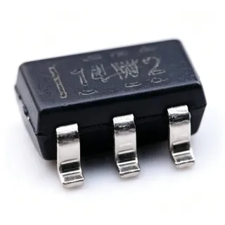
OPA335AIDBVR - Zero-Drift 5uV Op Amp, 2MHz, SOT-23-5 | TI
N.º de pieza: OPA335AIDBVR ✓ Activo| Cant. | Precio unitario | Total |
|---|---|---|
| 1 | $2.45 | $2,45 |
| 10 | $2.18 | $21,80 |
| 100 | $1.86 | $186,00 |
| 500 | $1.62 | $810,00 |
| 1.000 | $1.41 | $1.410,00 |
| 3.000 | $1.18 | $3.540,00 |
OPA335AIDBVR Descripción general
A zero-drift operational amplifier is a type of precision analog amplifier that uses internal auto-zeroing or chopper-stabilization techniques to continuously cancel the input-offset voltage and its variation with temperature. Within the broader signal-chain hierarchy, an op amp functions as the fundamental active building block for amplification, filtering, and signal translation; precision zero-drift variants sit at the top of that taxonomy (precision op amp -> operational amplifier -> amplifier -> analog IC -> semiconductor). Compared to conventional CMOS op amps whose offset can drift tens of microvolts over temperature, the OPA335 holds sub-microvolt drift over the full -40C to +125C range, eliminating periodic calibration in many instrumentation paths.
Key features include 285 uA typical quiescent current, 2 kV HBM ESD on the input pins, unity-gain stable operation with 1 nF capacitive loads, and rail-to-rail output that swings within 30 mV of either supply at 10 kohm loading. The TI proprietary auto-zero architecture produces no chopping artifacts in the audio band, allowing clean thermopile and strain-gauge signal chains. Internal RFI/EMI rejection filtering at the inputs suppresses out-of-band interference from cellular, Wi-Fi, or motor-drive sources without external RC networks.
The OPA335 pairs an internal precision oscillator with switched-capacitor nulling to dynamically measure and correct offset every clock cycle. This architecture removes the 1/f noise that dominates low-frequency CMOS amplifiers and creates a flat noise spectral density down to DC. Because the device operates from a single supply, designers can omit the negative rail that traditional bipolar precision amplifiers require, saving PCB area and BOM cost.
Typical applications include thermocouple and RTD front-ends, load-cell conditioning for weighing scales, precision current sensing for battery monitors, medical instrumentation such as glucose meters, and handheld industrial test equipment. The 2.7 V minimum supply also enables direct 3.3 V system integration with MCUs and ADCs.
When laying out the OPA335, keep input traces short and guarded, route the high-impedance nodes away from switching nodes, and place the 0.1 uF supply bypass within 3 mm of the V+ pin. Designers should avoid placing large capacitive loads directly at the output - the amplifier remains stable with up to 1 nF but rapidly loses phase margin above that.
This page synthesizes distributor pricing, drop-in SOT-23-5 alternatives, and practical layout notes from the manufacturer datasheet, providing comparison and selection context not available on a single-line distributor listing.
Alternativas directas para OPA335AIDBVR — mismo encapsulado, compatible pin a pin. Se excluyen las piezas de otro encapsulado que requieren retrabajo de la PCB.
Variantes de esta serie
Modelos de la misma serie compatibles directamente con OPA335AIDBVR (mismo factor de forma y huella) — difiere en Amplifier Type, Operating Temperature Range, Package, Slew Rate.
Herramienta de comparación rápida — seleccione piezas alternativas para compararlas lado a lado:
OPA334AIDBVR
✅ Sustitución directa📋 Alternativa de referencia (no en el catálogo)
OPA330AIDBVR
✅ Sustitución directa📋 Alternativa de referencia (no en el catálogo)
OPA335AIDBVT
✅ Sustitución directa📋 Alternativa de referencia (no en el catálogo)
OPA335AID
✅ Sustitución directa ⚠️ Especificaciones sin verificar📋 Alternativa de referencia (no en el catálogo)
AD8628ARTZ-REEL7
✅ Sustitución directa✓ En stock
$1.85 / unidad
Ver hoja de datos →MAX44260AUD+T
✅ Sustitución directa📋 Alternativa de referencia (no en el catálogo)
OPA335AIDBVR Valores máximos y características eléctricas
| Amplifier Type | Zero-Drift, Precision, Auto-Zero |
| Number of Channels | 1 |
| Maximum Offset Voltage (VOS) | 5 uV (at 25C) |
| Maximum Offset Voltage Drift (dVOS/dT) | 0.05 uV/C |
| Gain-Bandwidth Product (GBW) | 2 MHz |
| Slew Rate | 1.6 V/us |
| Supply Voltage Range (Single Supply) | 2.7 V to 5.5 V |
| Quiescent Current (IQ) | 285 uA typical |
| Tipo de salida | Rail-to-Rail Output |
| Output Swing (10 kohm load) | Within 30 mV of either rail |
| Rango de temperatura de funcionamiento | -40C to +125C |
| ESD Rating (HBM) | 2 kV |
| Shutdown Pin | No (OPA334 variant has shutdown) |
| Encapsulado | SOT-23-5 (DBV) |
| Tipo de montaje | Surface Mount |
| Estado RoHS | Compliant |
| Número de pines | 5 |
Configuración de pines de OPA335AIDBVR
| Pin 1 | NC — No internal connection (OPA335 has no shutdown feature; pin is floating) |
| Pin 2 | IN- — Inverting input |
| Pin 3 | IN+ — Non-inverting input |
| Pin 4 | V- — Negative supply (ground for single-supply operation) |
| Pin 5 | V+ — Positive supply (2.7 V to 5.5 V) |
Aplicaciones típicas
OPA335AIDBVR es adecuado para 7 aplicacións: Thermocouple and RTD Front-End Amplification, Load-Cell and Weigh-Scale Signal Conditioning, Precision Current Sensing for Battery Monitors, Handheld Medical Instrumentation, Precision Active Filters, Industrial Sensor Transmitter Outputs, Test and Measurement Instrumentation Front-End.
Thermocouple and RTD Front-End Amplification
The OPA335AIDBVR excels in thermocouple and RTD front-ends because its 5 uV maximum input offset voltage and 0.05 uV/C maximum offset drift remain well below the 40 uV/C Seebeck coefficient of a K-type thermocouple across the industrial -40C to +125C range. The amplifier's near-zero 1/f noise corner eliminates the low-frequency noise that swamps millivolt-level temperature signals. Placed as the first gain stage with a precision resistor network, the OPA335 provides drift-free amplification directly to a 16 to 24-bit ADC without software recalibration, simplifying firmware on cost-sensitive industrial controllers.
Recomendado
Load-Cell and Weigh-Scale Signal Conditioning
In load-cell and weigh-scale designs, the OPA335AIDBVR is wired as a differential gain stage amplifying the few-millivolt full-bridge output of a strain gauge. The auto-zeroing architecture keeps offset drift below 0.05 uV/C, which is critical because mechanical scales must hold calibration over months of operation without user recalibration. With a 2 MHz gain-bandwidth the amplifier settles quickly for fast weighing cycles, and its 285 uA quiescent current suits battery-powered portable scales. Designers typically pair it with a 24-bit sigma-delta ADC such as the TI ADS1231 to digitise the bridge signal directly.
Recomendado
Precision Current Sensing for Battery Monitors
The OPA335AIDBVR's near-zero offset voltage makes it ideal for high-side or low-side current sensing in battery monitors where a 5 uV offset at a 100 milliohm shunt produces only 50 uA of measurement error - far below the milliamp-level State-of-Charge transitions that govern battery-pack controllers. The 2.7 V to 5.5 V supply range aligns with single-cell Li-ion and multi-cell NiMH packs, while the rail-to-rail output maximises dynamic range when sensing current on a low-voltage rail. Compared to a chopper amplifier the OPA335 produces no switching ripple that could couple into adjacent coulomb-counting ADCs.
Recomendado
Handheld Medical Instrumentation
The OPA335AIDBVR supports handheld medical devices such as glucose meters, pulse oximeters, and spot-check ECG front-ends by providing a low-noise, low-drift first stage for microvolt-level biosignals. The 285 uA quiescent current preserves battery life on coin cells, and the SOT-23-5 footprint fits the dense PCB real estate of handheld enclosures. Its EMI/RFI input filter suppresses interference from Wi-Fi, Bluetooth, or cellular radios used in connected health devices. Designers typically pair the OPA335 with a 16 to 24-bit ADC to digitise the conditioned biosignal for clinical-grade accuracy.
Recomendado
Precision Active Filters
The OPA335AIDBVR is well suited to high-order Sallen-Key or multiple-feedback active filters where sub-millivolt DC accuracy must coexist with clean audio-band response. The auto-zeroing topology keeps the filter's passband ripple and DC output stable over temperature, eliminating the gain-error drift that plagues conventional CMOS op amps below 10 Hz. Combined with 2 MHz gain-bandwidth, the amplifier supports filter cutoffs up to several hundred kilohertz in audio, seismic, or vibration-sensing applications.
Recomendado
Industrial Sensor Transmitter Outputs
In 4-20 mA industrial sensor transmitters and PLC analog output modules, the OPA335AIDBVR drives the loop or DAC with sub-microvolt drift, ensuring that the output current or voltage remains within the 0.1 percent accuracy class across the operating temperature range. The 5 V single-supple operation simplifies the field-side power architecture, while the SOT-23-5 footprint enables extremely compact DIN-rail transmitter designs. Compared to legacy bipolar amplifiers the OPA335 also reduces BOM cost by eliminating the negative voltage rail typically required for output swing near 0 V.
Recomendado
Test and Measurement Instrumentation Front-End
Test and measurement instruments such as benchtop multimeters, data-acquisition modules, and laboratory-grade signal sources rely on the OPA335AIDBVR's 5 uV offset and 2 MHz gain-bandwidth to provide repeatable DC and low-frequency AC measurements. The near-zero drift eliminates the need to recalibrate the instrument after warm-up, shortening test time. The SOT-23-5 footprint also enables dense channel counts in multi-channel DAQ cards where hundreds of amplifier stages compete for PCB real estate. Engineers pair it with high-resolution ADCs such as the ADS1262/63 for sub-ppm DC measurement accuracy.
Recomendado
Resumen de productos recomendados
Datos de referencia de ingeniería para OPA335AIDBVR — comparación, orientación de diseño e información de cumplimiento.
Guía de selección
Comparación con alternativas
| Parámetro | Este producto | OPA334AIDBVR | OPA330AIDBVR | OPA335AIDBVT | OPA335AID | AD8628ARTZ-REEL7 | MAX44260AUD+T |
|---|---|---|---|---|---|---|---|
| Brand | Texas Instruments | Texas Instruments | Texas Instruments | Texas Instruments | Texas Instruments | Analog Devices | Analog Devices |
| Package | SOT-23-5 (DBV) | SOT-23-5 (DBV) - same | SOT-23-5 (DBV) - same | SOT-23-5 (DBV) - same | SOT-23-5 (DBV) - same | SOT-23-5 equivalent - same | SOT-23-5 equivalent - same |
| Channels | 1 | 1 | 1 | 1 | 1 | 1 | 1 |
| Offset Voltage (max) | 5 uV | 5 uV | 50 uV | 5 uV | 5 uV | 5 uV | 50 uV |
| Gain-Bandwidth Product | 2 MHz | 2 MHz | 0.35 MHz (lower) | 2 MHz | 2 MHz | 2.5 MHz | 1.5 MHz |
| Supply Voltage Range | 2.7 V to 5.5 V | 2.7 V to 5.5 V | 1.8 V to 5.5 V (wider) | 2.7 V to 5.5 V | 2.7 V to 5.5 V | 2.7 V to 13 V (wider) | 1.8 V to 5.5 V (wider) |
| Output Swing | Rail-to-Rail | Rail-to-Rail | Rail-to-Rail | Rail-to-Rail | Rail-to-Rail | Rail-to-Rail | Rail-to-Rail |
| Shutdown Pin | No | Yes (pin 1 enable) | No | No | No | No | No |
Diferenciadores clave
- Higher gain-bandwidth for precision AC applications (frente a OPA330AIDBVR)
- Lower offset voltage than OPA330 family (frente a OPA330AIDBVR)
- No shutdown pin simplifies always-on designs (frente a OPA334AIDBVR)
- Cross-brand precision alternative with wider supply (frente a AD8628ARTZ-REEL7)
Notas de diseño
Estimated: place a 0.1 uF X7R ceramic bypass capacitor within 3 mm of the V+ pin (pin 5) using a short, wide trace; add a 1 uF to 10 uF bulk capacitor adjacent to the amplifier supply rail. The SOT-23-5 package has only one thermal pad lead on V- (pin 4), so pour a copper plane on the V- layer directly under the device to act as both ground return and thermal relief. Avoid routing input traces parallel to switching nodes (DC-DC converters, motor drivers) - the OPA335's auto-zero architecture will still couple switching noise into the input even though the integrated EMI filter provides some rejection.
Do not place a load capacitance greater than approximately 1 nF directly at the output - the amplifier remains unity-gain stable to 1 nF but rapidly loses phase margin above that. If your circuit requires a larger output capacitor (for example, a cable or ADC reference bypass), isolate it with a 10 ohm to 100 ohm series resistor. Also avoid operating the input common-mode voltage within 1 V of the positive rail at high temperature; consult the input common-mode range vs. V+ plot in the manufacturer datasheet before finalising the design.
Estimated: the OPA335 in SOT-23-5 dissipates roughly 1.4 mW at 285 uA quiescent and 5 V supply, giving a junction temperature rise of about 0.36 C above ambient assuming the standard 260 C/W theta_JA for a JEDEC EIA/JESD51 4-layer test board. Because power dissipation is negligible, no special thermal relief is required beyond a small ground copper pour. For dual-layer 1 oz boards without an internal power plane, the theta_JA can exceed 400 C/W and the result remains thermally safe - the OPA335 is not a thermally constrained op amp even on minimal PCB real estate.
For strain-gauge or load-cell applications the OPA335 should be paired with a guard ring driven by the same output node (when operating as a unity-gain buffer) or by a low-impedance reference (when configured as an inverting amplifier). The guard ring intercepts leakage currents from the high-impedance input PCB surface and is critical when the input impedance exceeds 1 Gohm or the operating temperature is above 60C. Use a star-ground topology at the OPA335 V- pin to avoid ground-loop noise coupling into the bridge return path.
Información de cumplimiento
RoHS and REACH compliant per Arrow and DigiKey distributor listings. Not AEC-Q100 qualified - choose OPA335AIDBVR-Q1 for automotive applications if available.