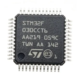
STM32H753BIT6 - 480MHz Cortex-M7 MCU, 2MB Flash, LQFP-208 | STMicroelectronics
N.º de pieza: STM32H753BIT6 ✓ ActivoSTM32H753BIT6 Descripción general
A microcontroller is a single integrated circuit that contains a processor core, memory, and peripherals on one die, and it forms the lowest tier of the embedded computing hierarchy: MCU -> embedded processor -> system-on-chip -> embedded computing platform. In that hierarchy, a Cortex-M7 MCU such as this one targets high-end control, networking, and human-machine-interface duties that sit above typical 8-bit or Cortex-M0/M3 devices but below application processors running Linux.
Key features of this part include a 480 MHz Arm Cortex-M7 core with double-precision FPU and DSP instructions, 2 MB of on-chip Flash for firmware and assets, 1 MB of on-chip SRAM, an instruction cache and data cache, and a hardware cryptographic accelerator for AES and SHA. The 168 available I/O lines make it possible to attach displays, Ethernet or SDIO peripherals, motor-control outputs, and multiple sensor buses without external I/O expanders, while the large LQFP-208 footprint exposes both FMC interfaces for external SDRAM and QSPI NOR flash.
Architecturally, the STM32H753 belongs to the STM32H7 family, which combines a very high-bandwidth AXI matrix with multiple DMA controllers and a ChromeART accelerator for 2D graphics and video. The device is configured by the STM32CubeMX toolchain and programmed through SWD/JTAG debug interfaces, with firmware secured through the cryptographic accelerator and hardware unique key.
Typical applications include industrial HMI panels with TFT-LCD and capacitive touch, industrial Ethernet gateways, motor-control and servo drives, building automation controllers, medical monitoring stations, and edge AI image-processing front ends where the 2 MB Flash and 1 MB RAM allow substantial local buffering.
A key design consideration is power-domain planning. Unlike the earlier STM32F7 series with an external BYPASS_REG pin, the STM32H753 uses an internal LDO and optional SMPS with software-configurable scaling, so rail sequencing must be programmed in the power-management initialization sequence rather than by hardware pin straps. Decoupling requirements at VDD and VDDCORE follow the datasheet reference layout.
This page brings together package, memory, and interface details, pin-compatible alternatives from the STM32H7 family, and practical integration notes that are not consolidated anywhere else in a single reference.
Alternativas directas para STM32H753BIT6 — mismo encapsulado, compatible pin a pin. Se excluyen las piezas de otro encapsulado que requieren retrabajo de la PCB.
Variantes de esta serie
Modelos de la misma serie compatibles directamente con STM32H753BIT6 (mismo factor de forma y huella) — difiere en Package, Communication Interfaces, Flash Memory, Number of I/O Pins, SRAM.
STM32H743BIT6
✅ Sustitución directa ⚠️ Especificaciones sin verificar✗ Sin stock
$9.85 / unidad
Ver hoja de datos →STM32H750BIT6
✅ Sustitución directa📋 Alternativa de referencia (no en el catálogo)
STM32H733BIT6
✅ Sustitución directa ⚠️ Especificaciones sin verificar📋 Alternativa de referencia (no en el catálogo)
STM32H723BIT6
✅ Sustitución directa ⚠️ Especificaciones sin verificar📋 Alternativa de referencia (no en el catálogo)
STM32H725BIT6
✅ Sustitución directa ⚠️ Especificaciones sin verificar📋 Alternativa de referencia (no en el catálogo)
STM32H735BIT6
✅ Sustitución directa ⚠️ Especificaciones sin verificar📋 Alternativa de referencia (no en el catálogo)
STM32H753BIT6 Valores máximos y características eléctricas
| Manufacturer | STMicroelectronics |
| Product Type | 32-bit ARM Microcontroller (MCU) |
| CPU Core | Arm Cortex-M7 with FPU and DSP instructions |
| Maximum CPU Frequency | 480 MHz |
| Architecture | 32-bit RISC |
| Flash Memory Size | 2 MB (2M x 8) |
| RAM Size | 1 MB |
| Encapsulado | LQFP-208 (28 x 28 mm), also listed as PQFP-208 |
| Number of I/O Pins | 168 |
| Tipo de montaje | Surface Mount |
| Series | STM32H7 Series, STM32H753xI line |
| Core Count | Single core |
| Caches | Instruction cache and data cache, Cortex-M7 architecture |
| Crypto Accelerator | Hardware AES and SHA accelerator (STM32H7 family feature) |
| Programming Interface | SWD / JTAG debug |
| Toolchain Support | STM32CubeMX, STM32CubeIDE, Arm Keil, IAR Embedded Workbench |
| External Memory Interfaces | FMC for SDRAM and QSPI NOR/NAND devices |
| Packaging Type | Tray |
Guía de configuración de pines de STM32H753BIT6 lqfp-208 (28 x 28 mm), also listed as pqfp-208
Configuración de pines para STM32H753BIT6 (encapsulado lqfp-208 (28 x 28 mm), also listed as pqfp-208). Este CI digital incluye GPIO, interfaces de comunicación (UART, SPI, I2C) y pines de alimentación. Consulte la hoja de datos del fabricante para conocer las funciones alternativas de los pines y las opciones de configuración. Esencial para el diseño de sistemas embebidos y el diseño de PCB.

No hay datos detallados de patillaje disponibles para STM32H753BIT6.
Consulte la hoja de datos para ver la configuración completa de patillas.
Aplicaciones típicas
STM32H753BIT6 es adecuado para 6 aplicacións: Industrial HMI and Machine Panels, Industrial Ethernet Gateways and Protocol Hubs, Motor Control and Servo Drives, Edge AI Vision and Image Processing Front Ends, Building Automation and HVAC Controllers, Medical and Diagnostic Monitoring Equipment.
Industrial HMI and Machine Panels
The STM32H753BIT6 fits graphical operator panels because its 480 MHz Cortex-M7 core drives the ChromeART accelerator for 2D and video compositing while 1 MB of RAM holds double-frame buffers for a 480x800 TFT-LCD. The 168 I/O lines allow parallel RGB display data, resistive or capacitive touch controller lines, and keypad scanning on one MCU, and the 2 MB of Flash stores fonts, bitmaps, and multilingual string tables. Because panels often run an RTOS plus graphics stack, the 64 KB data cache and 128 KB instruction cache keep external QSPI flash and SDRAM accesses from stalling the pipeline.
Recomendado
Industrial Ethernet Gateways and Protocol Hubs
A protocol gateway needs to run TCP/IP stacks, TLS sessions, and multiple fieldbus tasks concurrently, which is where the 480 MHz Cortex-M7 of the STM32H753BIT6 earns its keep. The hardware cryptographic accelerator handles AES and SHA operations for secure fieldbus tunnels without loading the core, and the 2 MB of Flash allows dual image storage for field updates, while 1 MB of RAM supports multiple socket buffers and DMA descriptors for Ethernet, CAN-FD, and RS-485 transceivers. The 208-pin LQFP exposes the FMC interface so external SDRAM can be added when buffer depth must grow.
Recomendado
Motor Control and Servo Drives
The STM32H753BIT6 is suited to servo and stepper drives because the high-bandwidth AXI interconnect and advanced timer architecture support fast PWM generation, encoder and resolver interfaces, and deterministic current-loop timing at 480 MHz. The hardware FPU with DSP instructions accelerates the transform and filter stages of field-oriented control, and 1 MB of RAM is enough to hold multiple current, velocity, and position loops simultaneously. With 168 I/O lines, dead-time insertion, brake inputs, and Hall or encoder channels are handled without adding logic devices between the MCU and the power stage.
Recomendado
Edge AI Vision and Image Processing Front Ends
Machine-vision and inspection cameras use the STM32H753BIT6 as a front-end processor when the imaging pipeline must be handled on-device rather than in the cloud. The Cortex-M7 with its DSP extensions performs pre-processing such as filtering, thresholding, and colour-space conversion at 480 MHz, the ChromeART accelerator handles the 2D composition and scaling stages, and 1 MB of RAM accommodates a working frame buffer. The 208-pin LQFP also provides a CSI-style sensor interface plus plenty of digital I/O to trigger strobes and drive shutters, while 2 MB of Flash holds the model weights and inference code.
Recomendado
Building Automation and HVAC Controllers
Building controllers in this class juggle many slow buses and must survive years of unattended operation, and the STM32H753BIT6 provides both the compute margin and the peripheral breadth to do it. The 480 MHz core runs the supervisory task alongside communication stacks for BACnet, Modbus, KNX, or CAN, while 168 I/O lines cover relay outputs, triac firing, 0-10 V analog inputs, and NTC sensing directly. The hardware crypto accelerator secures controller-to-controller links and firmware update sessions, and 2 MB of Flash plus 1 MB of RAM allows long trend buffers and multiple protocol stacks to be resident simultaneously.
Recomendado
Medical and Diagnostic Monitoring Equipment
Diagnostic and patient-monitoring equipment benefits from the STM32H753BIT6 because it combines a deterministic 480 MHz core with strong on-chip security features and ample memory for signal conditioning software. The hardware cryptographic accelerator and unique device key support encrypted data links and authenticated firmware updates, which matters for devices handling protected health information. The 1 MB of RAM allows long acquisition buffers for waveform analysis, and the 168 I/O lines accept ECG front-end chip-selects, isolation barrier control, pump and valve drivers, and a local display plus keypad without extra logic.
Recomendado
Resumen de productos recomendados
Datos de referencia de ingeniería para STM32H753BIT6 — comparación, orientación de diseño e información de cumplimiento.
Guía de selección
Pick the STM32H743BIT6 as the closest same-package substitute when the H753-specific peripheral set is not required but you want identical core speed and memory. Pick the STM32H750BIT6 when security acceleration is unnecessary, since it shares the pin-compatible LQFP-208 footprint but drops the hardware crypto block. Pick the STM32H723BIT6 when cost dominates and your firmware fits comfortably inside a smaller memory budget.
Do not treat the STM32H755 as a drop-in, and do not plan on a cross-brand second source without a full board redesign: no NXP, Renesas, Microchip or GigaDevice part matches the 208-pin STM32H7 pinout.
Comparación con alternativas
| Parámetro | Este producto | STM32H743BIT6 | STM32H750BIT6 | STM32H733BIT6 | STM32H723BIT6 |
|---|---|---|---|---|---|
| Brand | STMicroelectronics | STMicroelectronics | STMicroelectronics | STMicroelectronics | STMicroelectronics |
| Package | LQFP-208 (28x28 mm) | LQFP-208 (28x28 mm) - same | LQFP-208 (28x28 mm) - same | LQFP-208 (28x28 mm) - same | LQFP-208 (28x28 mm) - same |
| CPU Core | Arm Cortex-M7, 32-bit RISC | Arm Cortex-M7, 32-bit RISC | Arm Cortex-M7, 32-bit RISC | Arm Cortex-M7, 32-bit RISC | Arm Cortex-M7, 32-bit RISC |
| Hardware Cryptographic Accelerator | Yes, AES and SHA hardware accelerator | Yes | No crypto accelerator in the H750 line | Yes | Yes |
| Development Ecosystem | STM32CubeMX, STM32CubeIDE, Keil MDK, IAR Embedded Workbench | STM32CubeMX, STM32CubeIDE, Keil MDK, IAR | STM32CubeMX, STM32CubeIDE, Keil MDK, IAR | STM32CubeMX, STM32CubeIDE, Keil MDK, IAR | STM32CubeMX, STM32CubeIDE, Keil MDK, IAR |
Diferenciadores clave
- Closest same-package substitute with identical core speed and memory (frente a STM32H743BIT6)
- Hardware crypto accelerator retained versus the H750 baseline (frente a STM32H750BIT6)
- Roughly double the memory of the reduced H723 option (frente a STM32H723BIT6)
- Highest I/O and memory density in the pin-compatible STM32H7 LQFP-208 group (frente a STM32H723BIT6)
Notas de diseño
The STM32H753 replaces the external BYPASS_REG arrangement used on older STM32F7 parts with an internal LDO and an optional SMPS whose voltage scaling is driven by software. Program the power-supply sequencing in the SystemClock_Config and regulator initialization code before enabling the high-speed domains, and make sure the VDDCORE and VDD rails are brought up in the order given in the datasheet power-supply sequence diagram. Do not assume the F7 bypass-capacitor arrangement carries over unchanged.
With 208 pins and 168 I/O lines, continuity of the power grid matters more than on smaller packages. Place the 100 nF ceramic decoupling capacitors directly at each VDD and VDDCORE pin rather than daisy-chaining a bank of bulk capacitance, and reserve a solid ground plane under the device. Route the SWDIO, SWCLK and NRST nets to a tag-connect footprint or 10-pin Cortex debug header so the board can be programmed without rework, and follow the ST recommended decoupling network on the analog supply and VREF pins.
Estimated: at a 3.3 V rail, a 480 MHz core running the DSP and FPU-heavy code in the STM32H753 can draw several hundred milliamperes of internal supply current. Using an assumed core current of 0.35 A at 3.3 V gives roughly 1.2 W of internal dissipation; with a typical large LQFP-208 junction-to-ambient resistance on a 4-layer board in the range of 25 to 35 C/W, the estimated junction temperature rise is about 30 to 42 C above ambient. Confirm actual dissipation with the ST thermal calculator for your package, pad, and board stack-up before fixing the ambient limit.
The most common substitution mistake is treating the STM32H755 as a drop-in for the STM32H753: STMicroelectronics community guidance states the LQFP STM32H755 is not pin compatible with the STM32H753 and STM32H750, so a last-minute swap can move power and signal nets. Second, the 480 MHz clocking requires correct PLL and voltage-scaling configuration, and using a stale CubeMX-generated clock tree silently drops the core to a lower frequency. Third, external QSPI flash and FMC SDRAM are not interchangeable, so verify the memory type on your board before substituting.
At 480 MHz with cache enabled, the AXI bus between core, caches, and DMA controllers becomes the bandwidth bottleneck for graphics and camera pipelines. Keep the external memory interface traces short, match length groups for QSPI and SDRAM, and place the memory close to the MCU. For camera or sensor links on the 168 available I/O lines, prefer the dedicated high-speed inputs rather than routing fast signals through the general-purpose GPIO matrix, and confirm the I/O speed settings in the GPIO configuration, since the default slew rate is optimised for low-frequency signals.
Información de cumplimiento
No explicit RoHS, REACH, or halogen-free declarations are published in the product documentation pages reviewed for this listing. The I ordering-code suffix denotes the industrial temperature grade; a dedicated AEC-Q100 automotive-grade variant exists separately in the STM32H7 line and is not this part. Confirm compliance documents for the exact ordering code when required for regulatory submission.