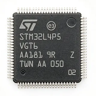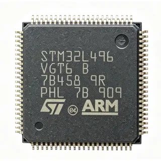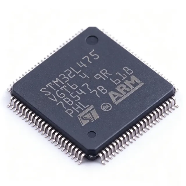
STM32L475VGT6 - 1MB Flash Cortex-M4 MCU, 100-LQFP | STMicroelectronics
N.º de pieza: STM32L475VGT6 ✓ Activo| Cant. | Precio unitario | Total |
|---|---|---|
| 1 | $9.5 | $9,50 |
| 10 | $8.55 | $85,50 |
| 100 | $7.3 | $730,00 |
| 500 | $6.4 | $3.200,00 |
| 1.000 | $5.85 | $5.850,00 |
| 3.000 | $5.2 | $15.600,00 |
STM32L475VGT6 Descripción general
A microcontroller (MCU) is a single-chip integrated circuit containing a processor core, program/data memory, and programmable peripherals that govern a specific embedded function. The STM32L475VGT6 is a member of the STM32L4 ultra-low-power family, which sits within the broader STM32 32-bit MCU portfolio and is engineered around ST's 110 nm ultra-low-leakage process with adaptive real-time (ART) accelerator. The Cortex-M4 core implements the ARMv7-M architecture with single-precision FPU and DSP extensions, making the part a member of the ARM Cortex-M family that is hierarchically classed as an embedded microcontroller -> 32-bit MCU -> semiconductor IC.
Key features include a wide 1.71 V to 3.6 V supply range, batch-collecting 12-bit 5 Msps ADC, two 12-bit DACs, two op-amps, two comparators, USB 2.0 OTG full-speed (with internal PHY), CAN 2.0B, SDMMC, SAI, DFSDM, multiple timers, and a true random number generator (TRNG) for security. Seven main low-power modes (Low-power Run, Sleep, Low-power Sleep, Stop 0/1/2, Standby, Shutdown) bring the typical Stop-mode current down to the microampere range and Standby/Shutdown to the nanoampere range, enabling multi-year battery life when paired with an energy-aware application design.
The architecture combines the Cortex-M4 DSP+FPUs with ST's ART Accelerator (instruction cache + pre-fetch) and an MPU, allowing sustained 100 DMIPS performance while maintaining ultra-low dynamic power. An embedded voltage regulator supports dynamic voltage scaling through the PDR1 (power-down) and LP regulator paths, decoupling core voltage from the external supply.
Typical applications include wearable fitness/health monitors, smart-metering and home/building automation nodes, industrial sensor hubs, medical point-of-care devices, low-power wireless IoT gateways, asset trackers, and USB-powered human-interface peripherals. The integrated USB OTG FS removes the need for an external PHY in many HID/CDC designs.
When designing with the STM32L475VGT6, follow the reference manual's decoupling and layout guidance (one 100 nF per VDD pair, one bulk 4.7 uF on the regulator input) and place the HSE crystal traces within the documented loading and guard-band limits. Selecting the right low-power pair must also consider whether the application can tolerate the wake-up latency of Stop 2 / Standby modes versus the higher autonomy of Low-power Run.
Alternativas directas para STM32L475VGT6 — mismo encapsulado, compatible pin a pin. Se excluyen las piezas de otro encapsulado que requieren retrabajo de la PCB.
Variantes de esta serie
Modelos de la misma serie compatibles directamente con STM32L475VGT6 (mismo factor de forma y huella) — difiere en Package, ADC, Core Architecture, DAC, USB.
Herramienta de comparación rápida — seleccione piezas alternativas para compararlas lado a lado:
STM32L476VGT6
✅ Sustitución directa✓ En stock
$4.09 / unidad
Ver hoja de datos →STM32L471ZGT6
✅ Sustitución directa✓ En stock
$7.49 / unidad
Ver hoja de datos →STM32L496RGT6
✅ Sustitución directa✓ En stock
$6.5 / unidad
Ver hoja de datos →GD32F450VGT6
✅ Sustitución directa📋 Alternativa de referencia (no en el catálogo)
GD32F470VGT6
✅ Sustitución directa📋 Alternativa de referencia (no en el catálogo)
STM32L475VGT6 Valores máximos y características eléctricas
| Core Architecture | ARM Cortex-M4 with FPU (32-bit) |
| Maximum CPU Clock | 80 MHz |
| Performance | 100 DMIPS |
| Flash Memory | 1 MB (1M x 8) |
| SRAM | 128 KB |
| Supply Voltage Range | 1.71 V to 3.6 V |
| Encapsulado | 100-LQFP (14x14 mm) |
| Temperatura de funcionamiento | -40 C to +85 C |
| ADC | 3x 12-bit, 5 Msps |
| DAC | 2x 12-bit |
| Comparators | 2x ultra-low-power |
| Op-Amps | 2x on-chip |
| USB | USB 2.0 OTG Full-Speed, integrated PHY |
| CAN | 1x CAN 2.0B |
| Communication Interfaces | I2C, SPI, USART, UART, SAI, SDMMC, DFSDM |
| Timers | 16-bit and 32-bit, multiple channels |
| Security | True Random Number Generator (TRNG), CRC |
| Low-Power Modes | Low-power Run, Stop 0/1/2, Standby, Shutdown |
| Estado RoHS | Compliant |
| Tipo de montaje | Surface Mount |
Configuración de pines de STM32L475VGT6
| Pin 1 | PE2 — GPIO PE2, TRACECLK |
| Pin 2 | PE3 — GPIO PE3, TRACED0 |
| Pin 3 | PE4 — GPIO PE4, TRACED1 |
| Pin 4 | PE5 — GPIO PE5, TRACED2 |
| Pin 5 | PE6 — GPIO PE6, TRACED3 |
| Pin 6 | VBAT — Battery backup supply |
| Pin 7 | PC13 — GPIO PC13, anti-tamper |
| Pin 8 | PC14 — OSC32_IN (LSE crystal) |
| Pin 9 | PC15 — OSC32_OUT (LSE crystal) |
| Pin 10 | VSS — Ground |
| Pin 11 | VDD — Digital supply 1.71-3.6 V |
| Pin 12 | PH0 — OSC_IN (HSE crystal) |
| Pin 13 | PH1 — OSC_OUT (HSE crystal) |
| Pin 14 | NRST — Active-low reset |
| Pin 15 | PC0 — GPIO PC0, ADC12_IN1 |
| Pin 16 | PC1 — GPIO PC1, ADC12_IN2 |
| Pin 17 | PC2 — GPIO PC2, ADC12_IN3 |
| Pin 18 | PC3 — GPIO PC3, ADC12_IN4 |
| Pin 19 | VSSA — Analog ground |
| Pin 20 | VREF+ — ADC reference voltage |
| Pin 21 | VDDA — Analog supply 1.71-3.6 V |
| Pin 22 | PA0 — GPIO PA0, ADC12_IN5, WKUP1 |
| Pin 23 | PA1 — GPIO PA1, ADC12_IN6 |
| Pin 24 | PA2 — GPIO PA2, USART2_TX |
| Pin 25 | PA3 — GPIO PA3, USART2_RX |
| Pin 26 | VSS — Ground |
| Pin 27 | VDD — Digital supply 1.71-3.6 V |
| Pin 28 | PA4 — GPIO PA4, SPI1_NSS, DAC1_OUT1 |
| Pin 29 | PA5 — GPIO PA5, SPI1_SCK, DAC1_OUT2 |
| Pin 30 | PA6 — GPIO PA6, SPI1_MISO, ADC12_IN11 |
| Pin 31 | PA7 — GPIO PA7, SPI1_MOSI, ADC12_IN12 |
| Pin 32 | PB0 — GPIO PB0, ADC12_IN15 |
| Pin 33 | PB1 — GPIO PB1, ADC12_IN16 |
| Pin 34 | PB2 — GPIO PB2, BOOT1 |
| Pin 35 | VSS — Ground |
| Pin 36 | VDD — Digital supply 1.71-3.6 V |
| Pin 37 | PB10 — GPIO PB10, I2C2_SCL, USART3_TX |
| Pin 38 | PB11 — GPIO PB11, I2C2_SDA, USART3_RX |
| Pin 39 | PB12 — GPIO PB12, SPI2_NSS |
| Pin 40 | PB13 — GPIO PB13, SPI2_SCK |
| Pin 41 | PB14 — GPIO PB14, SPI2_MISO |
| Pin 42 | PB15 — GPIO PB15, SPI2_MOSI |
| Pin 43 | PC6 — GPIO PC6, USART6_TX, TIM8_CH1 |
| Pin 44 | PC7 — GPIO PC7, USART6_RX, TIM8_CH2 |
| Pin 45 | PC8 — GPIO PC8, SDMMC1_D0, TIM8_CH3 |
| Pin 46 | PC9 — GPIO PC9, SDMMC1_D1, TIM8_CH4 |
| Pin 47 | PA8 — GPIO PA8, RCC_MCO_1, USART1_CK |
| Pin 48 | PA9 — GPIO PA9, USART1_TX |
| Pin 49 | PA10 — GPIO PA10, USART1_RX |
| Pin 50 | PA11 — GPIO PA11, USB_DM |
| Pin 51 | PA12 — GPIO PA12, USB_DP |
| Pin 52 | PA13 — GPIO PA13, SWDIO |
| Pin 53 | VSS — Ground |
| Pin 54 | VDD — Digital supply 1.71-3.6 V |
| Pin 55 | PA14 — GPIO PA14, SWCLK, JTCK |
| Pin 56 | PA15 — GPIO PA15, JTDI |
| Pin 57 | PC10 — GPIO PC10, SDMMC1_D2, USART3_TX |
| Pin 58 | PC11 — GPIO PC11, SDMMC1_D3, USART3_RX |
| Pin 59 | PC12 — GPIO PC12, SDMMC1_CK |
| Pin 60 | PD0 — GPIO PD0, CAN1_RX, FMC_D2 |
| Pin 61 | PD1 — GPIO PD1, CAN1_TX, FMC_D3 |
| Pin 62 | PD2 — GPIO PD2, SDMMC1_CMD |
| Pin 63 | PD3 — GPIO PD3, USART2_CTS |
| Pin 64 | PD4 — GPIO PD4, USART2_RTS |
| Pin 65 | PD5 — GPIO PD5, USART2_TX |
| Pin 66 | PD6 — GPIO PD6, USART2_RX |
| Pin 67 | PD7 — GPIO PD7, USART2_CK |
| Pin 68 | PB3 — GPIO PB3, JTDO, SWO, TIM2_CH2 |
| Pin 69 | PB4 — GPIO PB4, JTRST, TIM3_CH1 |
| Pin 70 | PB5 — GPIO PB5, I2C1_SMBAI, TIM3_CH2 |
| Pin 71 | PB6 — GPIO PB6, I2C1_SCL, USART1_TX |
| Pin 72 | PB7 — GPIO PB7, I2C1_SDA, USART1_RX |
| Pin 73 | BOOT0 — Boot mode selection |
| Pin 74 | PB8 — GPIO PB8, I2C1_SCL, CAN1_RX, TIM4_CH3 |
| Pin 75 | PB9 — GPIO PB9, I2C1_SDA, CAN1_TX, TIM4_CH4 |
| Pin 76 | VSS — Ground |
| Pin 77 | VDD — Digital supply 1.71-3.6 V |
| Pin 78 | PE7 — GPIO PE7, TIM1_ETR |
| Pin 79 | PE8 — GPIO PE8, TIM1_CH1N |
| Pin 80 | PE9 — GPIO PE9, TIM1_CH1 |
| Pin 81 | PE10 — GPIO PE10, TIM1_CH2N |
| Pin 82 | PE11 — GPIO PE11, TIM1_CH2 |
| Pin 83 | PE12 — GPIO PE12, TIM1_CH3N |
| Pin 84 | PE13 — GPIO PE13, TIM1_CH3 |
| Pin 85 | PE14 — GPIO PE14, TIM1_CH4 |
| Pin 86 | PE15 — GPIO PE15, TIM1_BKIN |
| Pin 87 | PA13 — GPIO PA13 (alternate pad location on LQFP-100, see datasheet) |
| Pin 88 | PC4 — GPIO PC4, USART3_TX |
| Pin 89 | PC5 — GPIO PC5, USART3_RX |
| Pin 90 | VSS — Ground |
| Pin 91 | VDD — Digital supply 1.71-3.6 V |
| Pin 92 | PB12 — GPIO PB12 (alternate, see datasheet) |
| Pin 93 | PB13 — GPIO PB13 (alternate, see datasheet) |
| Pin 94 | PB14 — GPIO PB14 (alternate, see datasheet) |
| Pin 95 | PB15 — GPIO PB15 (alternate, see datasheet) |
| Pin 96 | PA8 — GPIO PA8 (alternate, see datasheet) |
| Pin 97 | PA9 — GPIO PA9 (alternate, see datasheet) |
| Pin 98 | PA10 — GPIO PA10 (alternate, see datasheet) |
| Pin 99 | PA11 — GPIO PA11 (alternate, see datasheet) |
| Pin 100 | PA12 — GPIO PA12 (alternate, see datasheet) |
Aplicaciones típicas
STM32L475VGT6 es adecuado para 6 aplicacións: Wearable Health & Fitness Monitor, Smart Metering & Energy Harvesting Node, Industrial Sensor Hub with USB-C, Medical Point-of-Care Device, Low-Power IoT Gateway / Asset Tracker, Battery-Powered HMI / Keyboard.
Wearable Health & Fitness Monitor
The STM32L475VGT6 fits wearable health-and-fitness monitors because its Cortex-M4F DSP+FPU accelerates heart-rate, SpO2, and motion-sensor DSP pipelines while its ultra-low-power modes extend battery life. Stop 2 mode draws microampere-range quiescent current, allowing multi-week runtimes on a small Li-Po battery. The 12-bit 5 Msps ADC pairs with on-chip op-amps to condition bioimpedance and PPG signals without external analog front-ends. USB OTG FS with integrated PHY simplifies charging/CDC data synchronization with no external ULPI device. Recommended peripherals: STMicroelectronics LIS2DS12 accelerometer for motion context, STM32L476 companion for upgrade paths.
Recomendado
Smart Metering & Energy Harvesting Node
The STM32L475VGT6 fits smart-metering and energy-harvesting nodes because its 1.71-3.6 V supply range accepts direct output from small solar/PEM cells and its nanoampere Standby/Shutdown modes preserve battery during long idle windows. The Cortex-M4F runs metering DSP (RMS, harmonic analysis) at 80 MHz with 100 DMIPS headroom, and the SDMMC plus DFSDM peripherals interface to external metrology ASICs. Recommended companions: STMicroelectronics STPMIC1 power management IC, STM32L496RGT6 upgrade option with more SRAM.
Recomendado
Industrial Sensor Hub with USB-C
The STM32L475VGT6 fits industrial sensor hubs because its CAN 2.0B interface plus USB OTG FS provide both industrial bus connectivity and a USB-C host/device port for local HMI. Three 12-bit 5 Msps ADCs and two on-chip op-amps support multi-sensor analog front-ends without external amplifiers. The wide 1.71-3.6 V supply simplifies 24 V industrial-rail step-down to a single 3.3 V rail. Recommended companions: STMicroelectronics STM32F105RCT6 CAN bridge, STM32L073RZ for cost-down sensor-node designs.
Recomendado
Medical Point-of-Care Device
The STM32L475VGT6 fits medical point-of-care devices because its Cortex-M4F with FPU executes DSP-heavy signal-processing for ECG, pulse-oximetry, and impedance measurement in real time. The two 12-bit DACs and two on-chip op-amps condition analog front-end signals, while the SAI peripheral drives audio prompts or MEMS microphones. The TRNG provides the entropy source needed for authenticated firmware updates on medical hardware. Recommended companions: STMicroelectronics STM32H735IIT6 high-performance option, STM32L4R9ZIT6 for designs needing external SDRAM.
Recomendado
Low-Power IoT Gateway / Asset Tracker
The STM32L475VGT6 fits low-power IoT gateways and asset trackers because its USB OTG FS plus CAN, SDMMC, and SAI allow multiple wireless modules (LoRa, BLE, sub-GHz) to be hosted on a single MCU. Stop 2 mode draws microampere-level quiescent current when no events are pending, and the wide 1.71-3.6 V input tolerates battery droop during cold-temperature transients. Recommended companions: STMicroelectronics STM32MP135DAC3 for Linux-capable gateways, STM32F103VBT6 cost-down auxiliary.
Recomendado
Battery-Powered HMI / Keyboard
The STM32L475VGT6 fits battery-powered human-interface devices such as wireless keyboards, game controllers, and presenters because its low-power modes plus USB OTG FS (with integrated PHY) support both wireless 2.4 GHz dongles and USB-C wired modes. The 80 MHz Cortex-M4F runs HID report parsing and LED-matrix drivers in real time without external logic. Recommended companions: STMicroelectronics STM32G071G8U6 for ultra-low-cost wired-only HMI, STM32L051C8T3 for cost-sensitive button-only designs.
Recomendado
Resumen de productos recomendados
Datos de referencia de ingeniería para STM32L475VGT6 — comparación, orientación de diseño e información de cumplimiento.
Guía de selección
Comparación con alternativas
| Parámetro | Este producto | STM32L476VGT6 | STM32L471ZGT6 | GD32F450VGT6 | GD32F470VGT6 |
|---|---|---|---|---|---|
| Brand | STMicroelectronics | STMicroelectronics | STMicroelectronics | GigaDevice | GigaDevice |
| Package | 100-LQFP (14x14 mm) | 100-LQFP (14x14 mm) - same | 100-LQFP (14x14 mm) - same | 100-LQFP (14x14 mm) - same | 100-LQFP (14x14 mm) - same |
| Core | ARM Cortex-M4F @ 80 MHz | ARM Cortex-M4F @ 80 MHz | ARM Cortex-M4F @ 80 MHz | ARM Cortex-M4F @ 200 MHz | ARM Cortex-M4F @ 240 MHz |
| Flash | 1 MB | 1 MB | 1 MB | 1 MB | 1 MB |
| SRAM | 128 KB | 128 KB | 128 KB | 256 KB | 256 KB |
| USB OTG | Yes (FS, integrated PHY) | Yes (FS, integrated PHY) | Yes (FS, integrated PHY) | Yes (FS, integrated PHY) | Yes (FS/HS) |
| Hardware Crypto | TRNG + CRC | AES-256 + TRNG | TRNG + CRC | AES + TRNG | AES + TRNG |
| Stop Mode Current | Low (ultra-low-power family) | Low | Low | Higher than STM32L4 | Higher than STM32L4 |
| Supply Voltage Range | 1.71 V to 3.6 V | 1.71 V to 3.6 V | 1.71 V to 3.6 V | 2.6 V to 3.6 V | 2.6 V to 3.6 V |
| Unit Price (qty 1000) | $5.85 | Slightly higher than L475 | Comparable to L475 | Lower (cost-down option) | Lower (cost-down option) |
Diferenciadores clave
- Cortex-M4F with FPU at 80 MHz with 100 DMIPS and 7-mode ultra-low-power architecture (frente a STM32F103VBT6)
- Integrated USB OTG Full-Speed PHY (no external ULPI device required) (frente a GD32F450VGT6)
- AES-256 upgrade path in the same LQFP-100 footprint (frente a STM32L476VGT6)
Notas de diseño
Place one 100 nF decoupling capacitor as close as possible to each VDD pin and one bulk 4.7 uF ceramic at the regulator input (VDD/VDDA pair). According to the STM32L475xx datasheet power-supply section, using shared decoupling for the VDD/VDDA pins can couple digital switching transients into the analog reference and degrade ADC SNR by 4-6 dB. Use separate ferrite-bead-isolated rails for VDDA in metering and audio designs.
Route the HSE crystal traces within 7 mm of OSC_IN/OSC_OUT and keep the loading capacitors within the datasheet-specified CL range (typically 6-10 pF on STM32L4). Maintain a ground guard ring around the crystal and avoid routing signal traces under or near it; violating these rules typically causes HSE crystal-startup failures or 0.5-1% frequency error at temperature. Estimated crystal trace parasitic of 5 pF should be subtracted from the load-capacitor budget.
When migrating Stop 2 to Stop 0 for faster wake-up latency, the SDMMC, SAI, and DFSDM peripherals lose their configuration state and must be reinitialized in the wake-up ISR. Estimated wake-up time from Stop 2 is around 5-10 us vs 1 us from Stop 0; choose Stop 0 only when the application cannot tolerate the longer wake-up latency. Also note: Shutdown mode removes RTC backup register retention unless VBAT is held.
At 80 MHz active and 1.71-3.6 V supply, typical active current is approximately 10 mA / MHz giving 800 mW maximum at full CPU load on the 100-LQFP. The LQFP-100 has theta_JA around 50 C/W on a 4-layer JEDEC test board, so a 800 mW full-load dissipation yields about 40 C junction temperature rise above ambient; no heatsink is required for typical IoT workloads. Verify thermal rise at ambient 85 C to confirm Tjunction stays below 110 C.
Información de cumplimiento
RoHS and REACH compliant per ST product page. Standard grade is not AEC-Q100 qualified; choose AEC-Q100 qualified automotive variants (STM32L475RG-A) for automotive applications.