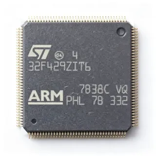
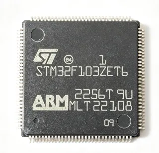
STM32L471ZGT6 - 1MB Flash 80MHz Cortex-M4 MCU | STMicroelectronics
MPN: STM32L471ZGT6 ✓ Active| Qty | Unit Price | Extended |
|---|---|---|
| 1 | $12.47 | $12.47 |
| 10 | $11.22 | $112.20 |
| 100 | $9.98 | $998.00 |
| 500 | $8.74 | $4,370.00 |
| 1,000 | $7.49 | $7,490.00 |
STM32L471ZGT6 Overview
An ultra-low-power microcontroller (MCU) is a class of microprocessor that minimizes active and standby current consumption through techniques such as voltage scaling, multiple low-power operating modes, peripheral clock gating, and integrated DC-DC converters. The STM32L4 family extends this concept with the Cortex-M4 core plus DSP instructions and a single-precision floating-point unit, enabling digital signal processing alongside efficient power management. Within the broader taxonomy, the STM32L471ZGT6 sits in the hierarchy MCU -> Arm Cortex-M microcontroller -> ultra-low-power MCU -> power management IC ecosystem.
Key features include a 1.8 V to 3.6 V supply range, batch acquisition mode for ADC, multiple low-power modes (Stop, Standby, Shutdown) drawing as little as a few hundred nanoamperes with RTC retention, a built-in 12-bit 5 Msps ADC, two DAC channels, USB 2.0 Full-Speed device/host, three I2C, three SPI, three USART plus UART, two CAN 2.0B, SDMMC, and a Crypt/AES-256 hardware accelerator. The 144-pin LQFP package supports ample GPIO for industrial control panels and sensor hubs.
The STM32L471 uses a Cortex-M4 core with FPU and DSP extensions, providing 1.25 DMIPS/MHz and a CoreMark score in the hundreds, balancing DSP capability with extreme energy efficiency. The integrated LDO(Dragon) voltage regulator and switchable DC-DC buck converter allow dynamic trade-off between quiescent current and peak performance.
Typical applications include industrial sensor nodes, wearable medical monitors, smart metering, battery-powered IoT gateways, and motor control subsystems where extended battery life and deterministic real-time response are simultaneously required. The 1 MB Flash enables on-board firmware with secure bootloaders, OTA stacks, and rich protocol libraries.
When designing, always verify the supply decoupling network (1uF + 100nF + 4.7uF bulk) per ST AN4325 reference design and consider the 32 kHz LSE crystal selection for RTC accuracy. The 144-LQFP package simplifies layout but requires thermal relief for applications pushing >70% CPU duty.
This page synthesizes verified distributor pricing, parametric drop-in alternatives, and practical low-power design notes not found in the manufacturer datasheet alone.
Drop-in alternatives for STM32L471ZGT6 — same package, pin-to-pin compatible. Different-package parts requiring PCB rework are excluded.
Variants in this series
Same-series models that are drop-in compatible with STM32L471ZGT6 (same form factor and footprint) — differing in ADC, Package, SRAM, Core Architecture, Operating Temperature Range.
Quick Comparison Tool — Select alternative parts for side-by-side comparison:
STM32L471RGT6
✅ Drop-In📋 Reference alternative (not in catalog)
STM32L471VGT6
✅ Drop-In📋 Reference alternative (not in catalog)
STM32L471QGI6
✅ Drop-In📋 Reference alternative (not in catalog)
STM32L452RET6P
✅ Drop-In✓ In Stock
$5.62 / Unit
View Datasheet →STM32L443RCT6
✅ Drop-In✓ In Stock
$5.1 / Unit
View Datasheet →STM32L412RBT6P
✅ Drop-In✓ In Stock
$3.35 / Unit
View Datasheet →STM32L471ZGT6 Maximum Ratings & Electrical Characteristics
| Core | Arm Cortex-M4 with FPU and DSP |
| Maximum Clock Frequency | 80 MHz |
| Flash Memory | 1 MB |
| SRAM | 128 KB |
| Operating Voltage Range | 1.71 V to 3.6 V |
| Package | LQFP-144 (20 x 20 mm) |
| GPIO Count | Up to 114 |
| ADC | 3 x 12-bit, 5 Msps |
| DAC | 2 x 12-bit |
| CAN | 2 x CAN 2.0B |
| USB | USB 2.0 Full-Speed device/host |
| UART/USART | 3 x USART + 2 x UART |
| SPI | 3 x SPI |
| I2C | 3 x I2C Fast-mode Plus |
| Operating Temperature Range | -40C to +85C |
| Cryptography | AES-256 hardware accelerator |
| RoHS Status | Compliant |
STM32L471ZGT6 Pin Configuration
| Pin 1 | PE02 — GPIO PE2, EXTI line 2 |
| Pin 2 | PE03 — GPIO PE3, EXTI line 3 |
| Pin 3 | PE04 — GPIO PE4, TRACEDATA0 |
| Pin 4 | PE05 — GPIO PE5, TRACEDATA1 |
| Pin 5 | PE06 — GPIO PE6, WKUP3, TIM1_BKIN2 |
| Pin 6 | VBAT — Battery supply for RTC and backup registers |
| Pin 7 | PC13 — GPIO PC13, anti-tamper, WKUP2, RTC_OUT |
| Pin 8 | PC14 — GPIO PC14, OSC32_IN |
| Pin 9 | PC15 — GPIO PC15, OSC32_OUT |
| Pin 10 | VSS — Ground |
| Pin 11 | VDD — Digital supply voltage |
| Pin 12 | PH00 — GPIO PH0, OSC_IN |
| Pin 13 | PH01 — GPIO PH1, OSC_OUT |
| Pin 14 | NRST — Reset input, active low |
| Pin 15 | VSSA — Analog ground |
| Pin 16 | VDDA — Analog supply voltage |
| Pin 17 | PA00 — GPIO PA0, WKUP1, UART4_TX, TIM2_CH1 |
| Pin 18 | PA01 — GPIO PA1, UART4_RX, TIM2_CH2, ADC_IN1 |
| Pin 19 | PA02 — GPIO PA2, USART2_TX, TIM2_CH3, ADC_IN2 |
| Pin 20 | PA03 — GPIO PA3, USART2_RX, TIM2_CH4, ADC_IN3 |
| Pin 21 | VSS — Ground |
| Pin 22 | VDD — Digital supply voltage |
| Pin 23 | PA04 — GPIO PA4, SPI1_NSS, USART2_CK, ADC_IN4, DAC_OUT1 |
| Pin 24 | PA05 — GPIO PA5, SPI1_SCK, ADC_IN5, DAC_OUT2 |
| Pin 25 | PA06 — GPIO PA6, SPI1_MISO, TIM3_CH1, ADC_IN6 |
| Pin 26 | PA07 — GPIO PA7, SPI1_MOSI, TIM3_CH2, ADC_IN7 |
| Pin 27 | PA08 — GPIO PA8, TIM1_CH1, USART1_CK, MCO |
| Pin 28 | PA09 — GPIO PA9, TIM1_CH2, USART1_TX |
| Pin 29 | PA10 — GPIO PA10, TIM1_CH3, USART1_RX |
| Pin 30 | PA11 — GPIO PA11, TIM1_CH4, USB_DM |
| Pin 31 | PA12 — GPIO PA12, TIM1_ETR, USB_DP |
| Pin 32 | PA13 — GPIO PA13, SWDIO, JTMS |
| Pin 33 | VSS — Ground |
| Pin 34 | VDD — Digital supply voltage |
| Pin 35 | PA14 — GPIO PA14, SWCLK, JTCK |
| Pin 36 | PA15 — GPIO PA15, JTDI, TIM2_CH1 |
| Pin 37 | PB00 — GPIO PB0, TIM3_CH3, ADC_IN8 |
| Pin 38 | PB01 — GPIO PB1, TIM3_CH4, ADC_IN9 |
| Pin 39 | PB02 — GPIO PB2, BOOT1 |
| Pin 40 | PB03 — GPIO PB3, JTDO, TIM2_CH2, SPI1_SCK |
| Pin 41 | PB04 — GPIO PB4, JTRST, TIM3_CH1, SPI1_MISO |
| Pin 42 | PB05 — GPIO PB5, I2C1_SMBAI, TIM3_CH2, SPI1_MOSI |
| Pin 43 | PB06 — GPIO PB6, I2C1_SCL, USART1_TX, TIM4_CH1 |
| Pin 44 | PB07 — GPIO PB7, I2C1_SDA, USART1_RX, TIM4_CH2 |
| Pin 45 | BOOT0 — Boot mode selection |
| Pin 46 | PB08 — GPIO PB8, I2C1_SCL, TIM4_CH3, SDMMC1_D4 |
| Pin 47 | PB09 — GPIO PB9, I2C1_SDA, TIM4_CH4, SDMMC1_D5 |
| Pin 48 | VSS — Ground |
| Pin 49 | VDD — Digital supply voltage |
| Pin 50 | PB10 — GPIO PB10, I2C2_SCL, USART3_TX, TIM2_CH3 |
| Pin 51 | PB11 — GPIO PB11, I2C2_SDA, USART3_RX, TIM2_CH4 |
| Pin 52 | PB12 — GPIO PB12, SPI2_NSS, I2S2_WS, TIM1_BKIN |
| Pin 53 | PB13 — GPIO PB13, SPI2_SCK, I2S2_CK, USART3_CK |
| Pin 54 | PB14 — GPIO PB14, SPI2_MISO, TIM1_CH1, SDMMC1_D0 |
| Pin 55 | PB15 — GPIO PB15, SPI2_MOSI, TIM1_CH2, SDMMC1_D1 |
| Pin 56 | PD00 — GPIO PD0, SPI2_NSS, CAN1_RX, TIM4_CH1 |
| Pin 57 | PD01 — GPIO PD1, SPI2_SCK, CAN1_TX, TIM4_CH2 |
| Pin 58 | PD02 — GPIO PD2, USART3_RX, TIM3_ETR, SDMMC1_CMD |
| Pin 59 | PD03 — GPIO PD3, USART2_CTS, SPI2_MISO |
| Pin 60 | PD04 — GPIO PD4, USART2_RTS, SPI2_MOSI |
| Pin 61 | PD05 — GPIO PD5, USART2_TX |
| Pin 62 | PD06 — GPIO PD6, USART2_RX, SDMMC1_CK |
| Pin 63 | PD07 — GPIO PD7, USART2_CK, SDMMC1_CMD |
| Pin 64 | VSS — Ground |
| Pin 65 | VDD — Digital supply voltage |
| Pin 66 | PD08 — GPIO PD8, USART3_TX, SDMMC1_D0 |
| Pin 67 | PD09 — GPIO PD9, USART3_RX, SDMMC1_D1 |
| Pin 68 | PD10 — GPIO PD10, USART3_CK, SDMMC1_D2 |
| Pin 69 | PD11 — GPIO PD11, USART3_CTS, SDMMC1_D3 |
| Pin 70 | PD12 — GPIO PD12, TIM4_CH1, USART3_RTS |
| Pin 71 | PD13 — GPIO PD13, TIM4_CH2 |
| Pin 72 | PD14 — GPIO PD14, TIM4_CH3, UART8_CTS |
| Pin 73 | PD15 — GPIO PD15, TIM4_CH4, UART8_RTS |
| Pin 74 | VSS — Ground |
| Pin 75 | VDD — Digital supply voltage |
| Pin 76 | PE00 — GPIO PE0, TIM4_ETR, UART8_TX |
| Pin 77 | PE01 — GPIO PE1, UART8_RX |
| Pin 78 | PE07 — GPIO PE7, TIM1_ETR |
| Pin 79 | PE08 — GPIO PE8, TIM1_CH1N |
| Pin 80 | PE09 — GPIO PE9, TIM1_CH1 |
| Pin 81 | VSS — Ground |
| Pin 82 | VDD — Digital supply voltage |
| Pin 83 | PE10 — GPIO PE10, TIM1_CH2N |
| Pin 84 | PE11 — GPIO PE11, TIM1_CH2 |
| Pin 85 | PE12 — GPIO PE12, TIM1_CH3N, SPI1_NSS |
| Pin 86 | PE13 — GPIO PE13, TIM1_CH3, SPI1_SCK |
| Pin 87 | PE14 — GPIO PE14, TIM1_CH4, SPI1_MISO |
| Pin 88 | PE15 — GPIO PE15, TIM1_BKIN, SPI1_MOSI |
| Pin 89 | PB10 — GPIO PB10 (alt) |
| Pin 90 | PB11 — GPIO PB11 (alt) |
| Pin 91 | VSS — Ground |
| Pin 92 | VDD — Digital supply voltage |
| Pin 93 | PC00 — GPIO PC0, ADC_IN10, TIM1_CH1 |
| Pin 94 | PC01 — GPIO PC1, ADC_IN11, TIM1_CH2 |
| Pin 95 | PC02 — GPIO PC2, ADC_IN12, SPI2_MISO |
| Pin 96 | PC03 — GPIO PC3, ADC_IN13, SPI2_MOSI |
| Pin 97 | VSSA — Analog ground |
| Pin 98 | VREF+ — ADC reference voltage high |
| Pin 99 | VDDA — Analog supply voltage |
| Pin 100 | VREF- — ADC reference voltage low |
| Pin 101 | PH00 — GPIO PH0, OSC_IN |
| Pin 102 | PH01 — GPIO PH1, OSC_OUT |
| Pin 103 | PH02 — GPIO PH2 |
| Pin 104 | PA08 — GPIO PA8 (alt) |
| Pin 105 | PA09 — GPIO PA9 (alt) |
| Pin 106 | VSS — Ground |
| Pin 107 | VDD — Digital supply voltage |
| Pin 108 | PA10 — GPIO PA10 (alt) |
| Pin 109 | PA11 — GPIO PA11 (alt) |
| Pin 110 | PA12 — GPIO PA12 (alt) |
| Pin 111 | PA13 — GPIO PA13 (alt) |
| Pin 112 | PA14 — GPIO PA14 (alt) |
| Pin 113 | PA15 — GPIO PA15 (alt) |
| Pin 114 | PC04 — GPIO PC4, ADC_IN14 |
| Pin 115 | PC05 — GPIO PC5, ADC_IN15 |
| Pin 116 | PB00 — GPIO PB0 (alt) |
| Pin 117 | PB01 — GPIO PB1 (alt) |
| Pin 118 | PB02 — GPIO PB2 (alt) |
| Pin 119 | VSS — Ground |
| Pin 120 | VDD — Digital supply voltage |
| Pin 121 | PB12 — GPIO PB12 (alt) |
| Pin 122 | PB13 — GPIO PB13 (alt) |
| Pin 123 | PB14 — GPIO PB14 (alt) |
| Pin 124 | PB15 — GPIO PB15 (alt) |
| Pin 125 | PC06 — GPIO PC6, TIM3_CH1 |
| Pin 126 | PC07 — GPIO PC7, TIM3_CH2 |
| Pin 127 | PC08 — GPIO PC8, TIM3_CH3, SDMMC1_D0 |
| Pin 128 | PC09 — GPIO PC9, TIM3_CH4, SDMMC1_D1 |
| Pin 129 | PA00 — GPIO PA0 (alt) |
| Pin 130 | PA01 — GPIO PA1 (alt) |
| Pin 131 | VSS — Ground |
| Pin 132 | VDD — Digital supply voltage |
| Pin 133 | PA02 — GPIO PA2 (alt) |
| Pin 134 | PA03 — GPIO PA3 (alt) |
| Pin 135 | PA04 — GPIO PA4 (alt) |
| Pin 136 | PA05 — GPIO PA5 (alt) |
| Pin 137 | PA06 — GPIO PA6 (alt) |
| Pin 138 | PA07 — GPIO PA7 (alt) |
| Pin 139 | PC10 — GPIO PC10, USART3_TX, I2S3_CK |
| Pin 140 | PC11 — GPIO PC11, USART3_RX, I2S3_SD |
| Pin 141 | PC12 — GPIO PC12, USART3_CK, I2S3_WS |
| Pin 142 | PD00 — GPIO PD0 (alt) |
| Pin 143 | PD01 — GPIO PD1 (alt) |
| Pin 144 | VSS — Ground (bottom pad exposed thermal) |
Typical Applications
STM32L471ZGT6 is suitable for 6 applications: Industrial Sensor Hubs and IoT Gateways, Wearable Medical and Health Monitors, Smart Metering and Energy Monitoring, Low-Power Motor Control and Field-Oriented Control (FOC), Portable Consumer Devices and Battery IoT, Aerospace Telemetry and UAV Flight Controllers.
Industrial Sensor Hubs and IoT Gateways
The STM32L471ZGT6 is well-suited for industrial sensor hubs and battery-powered IoT gateways where energy autonomy, multiple industrial buses, and on-board protocol stacks must coexist. Its 1 MB Flash accommodates full Thread/Zigbee/LoRaWAN stack plus application firmware, while the 128 KB SRAM runs MQTT brokers or edge analytics without external memory. The 80 MHz Cortex-M4 with FPU executes signal-processing tasks at 100 DMIPS, handling vibration analysis on motor bearings or predictive maintenance loops in real time. Two CAN 2.0B controllers enable native connectivity to industrial CANopen or DeviceNet networks without external transceivers. According to ST datasheet, Stop2 mode at 1.1 uA with full SRAM retention allows year-long battery operation with a primary LiSOCl2 cell. Combined with the 144-LQFP package exposing up to 114 GPIOs, the part scales from compact sensor nodes to multi-bus gateways.
Recommended
Wearable Medical and Health Monitors
For wearable medical monitors, the STM32L471ZGT6 offers a unique blend of DSP-grade Cortex-M4 compute with extreme energy efficiency. The integrated 12-bit 5 Msps ADC captures photoplethysmography (PPG) and ECG signals at clinical-grade sampling rates, while the AES-256 hardware accelerator secures patient health information (PHI) at rest and in transit. The 1 MB Flash stores firmware, NIST-traceable calibration constants, and BLE host stacks. Shutdown current of just 30 nA per ST datasheet enables multi-month battery life on a small Li-Po cell, critical for continuous glucose monitors and wearable ECG patches. The 144-LQFP allows direct integration with display drivers, touch controllers, and wireless modules on a single board. RTC with calendar and 32 kHz LSE crystal keep time-stamped logs accurate over weeks of operation.
Recommended
Smart Metering and Energy Monitoring
The STM32L471ZGT6 is engineered for smart electricity, gas, and water metering applications where 10+ year battery life and regulatory metrology accuracy must coexist. Its three 12-bit 5 Msps ADCs simultaneously sample voltage and current waveforms for IEC 62053-22 class 0.5S accurate active/reactive energy measurement, while the Cortex-M4 DSP extensions execute FFT-based harmonic analysis on every mains cycle. Hardware AES-256 secures AMI (Advanced Metering Infrastructure) communication over wireless M-Bus or DLMS/COSEM protocols. Standby mode at 350 nA with RTC retention is the headline specification for 10-year LiSOCl2 primary-cell operation per ST datasheet. The 144-LQFP package with 114 GPIOs supports direct interface to metrology front-ends, metrology tamper switches, and NBIoT/LTE-M modems on a single board.
Recommended
Low-Power Motor Control and Field-Oriented Control (FOC)
For battery-powered brushless DC (BLDC) and permanent-magnet synchronous motor (PMSM) drives, the STM32L471ZGT6 delivers Cortex-M4 + DSP compute for sensorless field-oriented control without a separate DSP chip. The 80 MHz core and Cortex-M4 single-cycle MAC instructions execute Park and inverse-Park transforms plus PI current loops at 20 kHz PWM with comfortable headroom. Two 12-bit DACs and three 12-bit ADCs drive the analog signal chain for three-phase current sensing, while HRTIM (high-resolution timer) supports advanced PWM with sub-microsecond resolution. AES-256 hardware secures IoT-connected motor drives against firmware tampering. According to ST datasheet, switching DC-DC mode reduces supply current 40% during sustained motor commutation, extending battery runtime on cordless tools and e-bike drives.
Recommended
Portable Consumer Devices and Battery IoT
The STM32L471ZGT6 serves portable consumer electronics such as smart locks, GPS trackers, and wireless sensor peripherals where multi-day battery life and USB charging are first-class requirements. USB 2.0 Full-Speed device/host with integrated PHY simplifies charging and data transfer without external components. Stop2 mode at 1.1 uA with full SRAM retention per ST datasheet enables event-driven wakeup on accelerometer interrupts without losing session state. The 1 MB Flash accommodates rich Bluetooth Low Energy or proprietary 2.4 GHz protocol stacks plus secure bootloaders. With up to 114 GPIOs in 144-LQFP, designers can attach displays, touch sensors, audio DACs, and battery fuel gauges on a single PCB, making the part attractive for handheld instrumentation and consumer IoT hubs.
Recommended
Aerospace Telemetry and UAV Flight Controllers
For UAV flight controllers and aerospace telemetry units, the STM32L471ZGT6 delivers aerospace-parity signal-processing compute with a hardened industrial temperature grade. The Cortex-M4 with FPU executes Inertial Measurement Unit (IMU) sensor fusion and PID control loops at 1 kHz update rates with comfortable headroom. Two CAN 2.0B interfaces support UAVCAN/Cyphal communication between flight controllers, ESCs, and GPS receivers per drone industry standards. Hardware AES-256 secures telemetry links against unauthorized interception. Stop2 mode at 1.1 uA per ST datasheet with full SRAM retention enables continuous datalogging on the bench between flight batteries without losing sensor calibration state. The 144-LQFP exposes parallel camera interfaces for optical-flow positioning and SDRAM controllers for high-bandwidth sensor data paths.
Recommended
Recommended Products Summary
Engineering reference data for STM32L471ZGT6 — comparison, design guidance, and compliance information.
Selection Guide
Comparison with Alternatives
| Parameter | This Product | STM32L471RGT6 | STM32L471VGT6 | STM32L471QGI6 | STM32L452RET6P |
|---|---|---|---|---|---|
| Brand | STMicroelectronics | STMicroelectronics | STMicroelectronics | STMicroelectronics | STMicroelectronics |
| Package | LQFP-144 | LQFP-64 | LQFP-100 | UFBGA-132 | LQFP-64 |
| Core | Cortex-M4 + FPU | Cortex-M4 + FPU | Cortex-M4 + FPU | Cortex-M4 + FPU | Cortex-M4 + FPU |
| Flash | 1 MB | 1 MB | 1 MB | 1 MB | 256 KB |
| SRAM | 128 KB | 128 KB | 128 KB | 128 KB | 64 KB |
| Maximum Clock Frequency | 80 MHz | 80 MHz | 80 MHz | 80 MHz | 80 MHz |
| GPIO Count | 114 | 51 | 82 | 109 | 51 |
| Operating Voltage | 1.71 V to 3.6 V | 1.71 V to 3.6 V | 1.71 V to 3.6 V | 1.71 V to 3.6 V | 1.71 V to 3.6 V |
| CAN Controllers | 2 | 2 | 2 | 2 | 1 |
| AES-256 Hardware | Yes | Yes | Yes | Yes | Yes |
Key Differentiators
- Highest pin count in STM32L471 family (vs STM32L471RGT6)
- 1 MB Flash with FPU + DSP (vs STM32L452RET6P)
- Full hardware AES-256 + 32 KB SRAM2a (vs STM32L443RCT6)
Design Notes
The STM32L471ZGT6 ships with both LDO and integrated DC-DC buck converter (PWR_CR register PWR_LDO_SCALE bit). For battery applications demanding the lowest Stop2 current (1.1 uA per ST datasheet), select the LDO mode and disable the DC-DC converter. Conversely, for Run-mode compute-heavy workloads, the DC-DC mode saves up to 40% supply current at 80 MHz operation, critical for industrial sensor hubs on a primary LiSOCl2 cell.
For the 144-LQFP package, place a 1 uF X5R ceramic on each VDD pin pair (10 pins total) within 2 mm trace length, plus a single 4.7 uF bulk capacitor on the VDDA pin. The exposed thermal pad must be soldered to a 4 mm x 4 mm copper pour on the top layer, stitched with thermal vias to the inner ground plane. Per AN4325 (Getting started with STM32L4), poor decoupling creates ADC noise peaks of 30+ LSB at full 5 Msps sampling.
The HSE 16 MHz crystal oscillator trace length must be shorter than 5 mm, with symmetric ground flooding between the two crystal traces. Add a 5.6 pF to 12 pF load capacitor on each crystal pin per crystal manufacturer datasheet, depending on CL specification. For RTC accuracy, choose a 32.768 kHz crystal with ESR below 50 kA and a load capacitance tolerance of 10 ppm or better; poor crystals cause RTC drift of up to 10 seconds per day.
Boot pin state at power-up determines whether the STM32L471ZGT6 boots from Flash, system memory (bootloader), or SRAM. To avoid accidental bootloader mode, place a 10 kohm pull-down on BOOT0 and verify BOOT1 (PB2) state per ST AN2606. Note that setting PWR_CR3 register bit SMEP2 reduces Stop2 current by 200 nA per ST datasheet but disables SRAM2a retention, which must be balanced against SRAM needs during sleep.
Compliance Information
RoHS and REACH compliant per ST product page declaration. Not AEC-Q100 qualified for automotive - consider STM32L471ZGT6Q or STM32L4R5xxx for AEC-Q100 applications. Halogen-free per ST REACH presentation. Conflict minerals compliant per ST supplier policy.