RF و بیسیم
زیردستهها
محصولات (700+)

SIM800C - Quad-Band GSM/GPRS Module | SIMCom
The SIM800C is a complete Quad-Band GSM/GPRS module in a compact LCC (Leadless Chip Carrier) package, designed by SIMCom Wireless Solutions. It operates on 850/900/1800/1900 MHz frequencies and supports GPRS data transfer up to 85.6 kbps. The module measures 17.6 x 15.7 x 2.3 mm, making it suitable for space-constrained IoT and embedded applications. It requires a supply voltage of 3.4V to 4.4V and features a 42-pin SMD interface. A GSM/GPRS module is a cellular communication module that enables devices to connect to GSM networks for voice, SMS, and data services. It integrates a baseband processor, RF transceiver, and power management into a single package, allowing developers to add cellular connectivity to their products without designing complex RF circuitry. The SIM800C sits within the hierarchy of cellular modules, which includes 2G, 3G, 4G LTE, and NB-IoT categories, and is specifically a 2G GSM/GPRS module. Key features of the SIM800C include support for Quad-Band frequencies, GPRS multi-slot class 12, and a rich set of interfaces including UART, USB 2.0, GPIO, SPI, and I2C. It also integrates an audio codec with speaker and microphone amplifiers, making it ideal for voice applications. The module supports AT command control, enabling easy integration with microcontrollers. Its low power consumption in sleep mode (around 1 mA) is beneficial for battery-powered devices. Technically, the SIM800C is built on a mature GSM/GPRS platform, offering reliable performance in 2G networks. It supports SMS, voice calls, and data transmission, with a maximum GPRS downlink speed of 85.6 kbps. The module includes a power management unit that handles over-voltage and under-voltage protection, ensuring safe operation. It also features a PWRKEY pin for power-on/off control and supports normal power-off via AT command 'AT+CPOWD=1'. Typical applications include remote monitoring, asset tracking, alarm systems, smart metering, and IoT gateways. Its compact size and low power consumption make it suitable for portable devices, while its robust interface set allows for flexible system integration. The SIM800C is widely used in industrial and consumer applications where 2G connectivity is still available. When designing with the SIM800C, ensure a stable power supply within 3.4V to 4.4V and adequate decoupling. The module requires a proper antenna connection and careful PCB layout to minimize RF interference. Also, consider the lifecycle status, as 2G networks are being phased out in many regions, which may affect long-term deployment.
SIM800C - Quad-Band GSM/GPRS Module | SIMCom | IoT & M2M
The SIM800C is a complete Quad-Band GSM/GPRS module in a compact LCC (Leadless Chip Carrier) package, designed by SIMCom Wireless Solutions. It operates on 850/900/1800/1900 MHz frequencies and supports GPRS data transfer up to 85.6 kbps. The module measures only 17.6 x 15.7 x 2.3 mm, making it ideal for space-constrained IoT and M2M applications. It provides a rich set of interfaces including UART, USB 2.0, GPIO, and an audio codec with speaker and microphone amplifiers, enabling voice, SMS, and data communication. A GSM/GPRS module is a self-contained cellular communication device that integrates a baseband processor, RF transceiver, and power management into a single package. It connects to a microcontroller via serial interfaces (typically UART) and communicates using AT commands. The SIM800C sits within the hierarchy: GSM/GPRS module -> cellular module -> wireless communication module -> IoT connectivity component. This modular approach simplifies adding cellular connectivity to embedded systems without requiring deep RF design expertise. Key features of the SIM800C include support for Quad-Band GSM/GPRS (850/900/1800/1900 MHz), GPRS class 12 (up to 85.6 kbps), and a wide operating voltage range of 3.4V to 4.4V. It integrates an audio codec and amplifiers for voice applications, and offers low power consumption in sleep mode (around 1 mA), which is critical for battery-powered IoT devices. The module also supports a variety of network protocols including TCP/IP, UDP, HTTP, and FTP via AT commands, enabling direct internet connectivity. Technically, the SIM800C uses a LCC package with 42 pins, providing excellent thermal and electrical performance. It includes a power management unit that handles over-voltage and under-voltage protection, and supports both normal and abnormal power-off procedures via the PWRKEY pin or AT command AT+CPOWD=1. The module is designed for easy integration with a minimal external component count, requiring only a power supply, SIM card holder, antenna, and a few passive components. Typical applications include remote monitoring and control systems, vehicle tracking devices, smart meters, alarm systems, and portable IoT devices. Its compact size and low power consumption make it suitable for battery-operated devices that need periodic data transmission. The SIM800C is also widely used in development boards and prototyping platforms. When designing with the SIM800C, ensure a stable power supply capable of handling current peaks up to 2A during GSM transmission bursts. Proper PCB layout with adequate grounding and decoupling is essential to maintain RF performance and minimize noise. Also, consider the module's lifecycle status, as it is being phased out in favor of 4G/LTE modules; for new designs, evaluate alternatives like the SIMCom A7683E or SIM7080G.
SIM868 - Quad-Band GSM/GPRS + GNSS Module | SIMCom
The SIMCom SIM868 is a quad-band GSM/GPRS cellular module with integrated GNSS satellite navigation (GPS/GLONASS/BDS), operating from a 3.4V to 4.4V supply with 650 uA idle current, housed in a compact 17.6 x 15.7 mm LCC/LGA surface-mount package. A GSM/GPRS module is a wireless communication subsystem that provides cellular voice, SMS, and packet-switched data connectivity over 2G mobile networks. Within the system hierarchy, it sits between the antenna/RF front end and the host microcontroller, abstracting the cellular protocol stack behind AT commands over UART. Modules such as the SIM868 belong to the broader family of cellular IoT modules, which also includes 3G, 4G/LTE, and LPWA (Cat-M/NB-IoT) devices. Key features include worldwide quad-band operation at 850/900/1800/1900 MHz, GPRS multi-slot class data rates up to 85.6 kbps in both downlink and uplink, and a co-located GNSS receiver supporting GPS, GLONASS, and BeiDou (BDS) constellations for positioning without a second module. The SIM868 integrates abundant extension interfaces: UART, USB 2.0, I2C, GPIO, dual SIM card interfaces, and an SD card interface. The dual-SIM capability is a differentiator versus the earlier SIM808, enabling multi-carrier failover designs. The compact LCC and LGA pad design significantly reduces development time and cost for GNSS-enabled M2M applications, and the module is ROHS compliant. Typical applications include asset tracking, vehicle fleet monitoring, anti-theft systems, and general M2M IoT devices that need both cellular telemetry and satellite positioning in a single footprint. Design considerations: supply the module from a low-impedance 3.4V to 4.4V rail capable of handling GSM transmit burst currents, and verify antenna keep-out areas in the 17.6 x 15.7 mm footprint region. This page synthesizes distributor pricing, availability, drop-in alternative analysis, and design notes not found in the manufacturer datasheet. According to the SIMCom product page, the SIM868 combines a complete quad-band GSM/GPRS engine with GNSS technology for satellite navigation.

SKY13522-644LF - 0.7-6 GHz SPDT RF Switch, 8-QFN | Skyworks
The Skyworks SKY13522-644LF is a single-pole, double-throw (SPDT) reflective RF switch covering 0.7 GHz to 6.0 GHz with 50 Ohm matching, housed in an 8-pin QFN (1.1 x 1.1 mm) surface-mount package. It delivers low insertion loss and high isolation suitable for cellular transmit/receive path routing, with single-bit GPIO control and 3 GHz maximum operating frequency in cellular band applications. An RF SPDT (single-pole double-throw) switch is a semiconductor routing element that selects one of two RF signal paths using a control voltage. SPDT switches belong to the broader category of RF switches -> RF front-end components -> wireless transceivers -> RF & wireless ICs. They are essential building blocks in time-division duplex (TDD) systems, antenna diversity modules, and band-selection filters, where a single antenna or filter bank must be shared between transmit and receive or between multiple bands. Key features include 0.7 GHz to 6.0 GHz operating range, 50 Ohm characteristic impedance, single-bit (one logic input) control interface, integrated DC blocking on the RF ports, and a compact 1.1 x 1.1 mm QFN-8 footprint. The advanced pHEMT switching technology maintains low insertion loss and high isolation across all switching paths, making the part well suited to cellular handset and module designs targeting GSM, CDMA, WCDMA, and LTE front-end sections. The device operates from a single supply and draws minimal DC current; the switch state is set by a single CMOS-compatible logic input, simplifying host-MCU or baseband GPIO integration. Internal ESD protection on the RF pins and the control input increases robustness during module assembly and field use. Typical applications include cellular handset transmit/receive switching, Wi-Fi 2.4 GHz and 5 GHz band routing, Bluetooth/BLE front-end switching, IoT and wearables antenna diversity, GPS L1 path selection, and reference designs for Wi-Fi + BLE combo modules. The broadband response also extends to 5 GHz Wi-Fi and sub-6 GHz industrial/scientific/medical bands. When designing with this part, place RF traces as 50 Ohm controlled-impedance lines and keep the VC1 control line routed away from sensitive RF traces to avoid digital-to-RF coupling. Decouple VDD close to the pin with a 1 nF to 100 pF combination; a typical application uses a single 1 nF X7R capacitor. This page synthesizes distributor pricing, EOL replacement guidance, drop-in alternatives, and practical design notes that complement the Skyworks manufacturer datasheet.
SKY13522-644LF-EVB - 0.7-3GHz SPDT Switch Evaluation Board | Skyworks
The Skyworks SKY13522-644LF-EVB is an evaluation board for the SKY13522-644LF single-pole, double-throw (SPDT) RF switch IC, covering the 0.7 GHz to 3 GHz frequency band with 50 ohm single-ended RF ports in a compact 8-QFN (1.1x1.1 mm) package. The host IC targets cellular front-end switching in CDMA, GSM, and WCDMA air interfaces and delivers high isolation of approximately 47 dB at 2.2 GHz, with low insertion loss supporting transmit/receive and band-switch routing. An RF switch (SPDT) is a semiconductor device that routes a single RF input to one of two RF output paths under logic-level CMOS control, enabling transmit/receive duplexing, antenna band selection, or diversity switching in a wireless front-end module. As part of the broader RF front-end (RFFE) hierarchy, the SPDT sits between the antenna or filter bank and the transceiver chain, and is typically controlled directly by the transceiver's GPIO or RFFE bus. Compared to mechanical relays, solid-state GaAs pHEMT-based SPDTs switch in tens of nanoseconds, draw only a few microamperes of quiescent current, and integrate into the same reflow-soldered PCB as the surrounding ICs. Key electrical characteristics of the underlying SKY13522-644LF device include a single-bit CMOS control interface that minimizes GPIO overhead, low insertion loss typically in the 0.4-0.6 dB range at 1-2 GHz, and high port-to-port isolation near 47 dB at 2.2 GHz, enabling signal chains to maintain dynamic range. The 50 ohm matched ports eliminate external matching networks and simplify board-level integration. The silicon implementation uses Skyworks' GaAs pHEMT switching process, which provides the linearity required for cellular power levels up to roughly +30 dBm, low DC power consumption with a few microamperes of quiescent current, and a single positive supply between approximately 2.5 V and 5.0 V. The 8-pin QFN (1.1 x 1.1 mm) exposed-pad package offers a low-inductance ground reference and excellent thermal performance for the small die area. The evaluation board hosts the IC on a calibrated FR4 substrate with SMA connectors and controlled-impedance traces so engineers can directly probe RF performance and control logic using standard laboratory instruments. Typical use cases for the SKY13522-644LF and its evaluation board include cellular handset transmit/receive switching, Wi-Fi/Bluetooth module antenna multiplexing, front-end module development for IoT and wearables, and reference designs for sub-6 GHz cellular and short-range radio platforms. The 0.7-3 GHz range matches cellular low-band, mid-band, 2.4 GHz ISM, and 2.6 GHz LTE/Wi-Fi bands. When designing with this part, drive the CMOS control pin from a clean logic rail (typically 1.8 V or 3.3 V) and place the control trace away from RF paths to avoid coupling. The exposed paddle of the QFN must be soldered to a continuous ground plane with multiple thermal vias for stable RF ground reference. This page synthesizes distributor availability, Skyworks' suggested replacement guidance, and EVB-related design notes that complement but do not replace the underlying SKY13522-644LF datasheet.
SKY66122-11 - 863-928MHz Wi-SUN RF Front End | Skyworks
The Skyworks Solutions SKY66122-11 is a high-performance, highly integrated RF front-end module (FEM) integrating a power amplifier (PA) and low-noise amplifier (LNA) for high-power 863 MHz to 928 MHz ISM band, Wi-SUN, and other IoT applications, housed in a 36-pin multi-chip module (MCM) package measuring 6x6 mm. An RF front-end module is a subsystem sitting between the radio transceiver IC and the antenna in a wireless signal chain. It typically combines a transmit-path power amplifier, a receive-path low-noise amplifier, RF switches for TX/RX switching, and a power detector for closed-loop output power control, all matched to 50 ohms so the system designer does not need external RF matching components. FEMs belong to the broader hierarchy of RF ICs, which includes transceivers, amplifiers, switches, and filters within the radio-frequency semiconductor family. Key features of the SKY66122-11 include fully matched 50 ohm RF input and output that eliminate external matching networks, digital control interfaces compatible with 1.6 V to 3.6 V CMOS logic levels for direct connection to common sub-GHz transceivers, an integrated RF switch for TX/RX path selection, and an integrated power detector that enables output power monitoring and closed-loop control. LCSC-listed features also cite an ultra-low 0.05 uA shutdown current, critical for battery-powered Wi-SUN and mesh nodes that sleep for most of their duty cycle. The integration of PA, LNA, switch, and coupler/detector in a single 6x6 mm MCM dramatically reduces board area compared with a discrete chain, and the internal inter-stage matching and harmonic filtering simplify compliance design for regional sub-GHz regulations in the 863-928 MHz band. The module is designed for ease of use and maximum flexibility, per the Skyworks product page. Typical applications include Wi-SUN mesh network routers and border routers, high-power ISM band telemetry, long-range Meshtastic and LoRa-style nodes (the part is used with the Semtech SX1262 in WisMesh high-power booster designs), smart metering, and street lighting control networks. Design consideration: as a high-power PA module, the SKY66122-11 requires attention to thermal pad grounding and supply decoupling; consult the manufacturer datasheet for the recommended PCB land pattern and thermal via array. This page synthesizes distributor pricing, availability, application context, and practical design notes not found in a single manufacturer datasheet.
SKY66122-11EK1 - 863-928MHz Wi-SUN FEM Eval Board | Skyworks
The Skyworks Solutions SKY66122-11EK1 is the official evaluation board for the SKY66122-11 high-performance RF front-end module (FEM), tuned for 863 to 915 MHz operation and intended for rapid prototyping of Wi-SUN, ISM-band, and IoT radio designs. An RF front-end module (FEM) evaluation board is a reference PCB that mounts the target RFIC together with the recommended matching network, decoupling, RF connectors, and control interfaces, allowing engineers to measure transmit power, receive sensitivity, and current consumption before committing to a custom layout. In the RF signal-chain hierarchy (evaluation board -> front-end module -> RF transceiver -> wireless node), the SKY66122-11EK1 sits at the top as a measurement and validation vehicle. The underlying SKY66122-11 FEM integrates a power amplifier, a low-noise amplifier (LNA), an RF switch, and a power detector in a single 36-pin MCM (6x6 mm) package. It provides fully matched 50 ohm RF input and output, digital control lines compatible with 1.6 V to 3 V logic, and supports the 863 to 928 MHz high-power ISM band for OFDM modulations such as Wi-SUN. Typical uses include bench characterization of output power and harmonic performance, link-budget validation for sub-GHz mesh networks, firmware development for radio controllers driving the digital control pins, and regulatory pre-scanning in the 863-928 MHz band. When using the board, maintain a clean low-noise supply and calibrate measurements with a calibrated vector signal analyzer to preserve result accuracy. This page synthesizes distributor pricing, datasheet references, and practical evaluation guidance not found in a single manufacturer page.
SKY66315-11 - 4.4-5GHz 5V RF Power Amp | Skyworks
The Skyworks SKY66315-11 is a high-efficiency, wide instantaneous bandwidth RF power amplifier (driver amp) designed for 4G LTE and 5G FDD/TDD systems operating from 4.4 GHz to 5 GHz, delivering approximately 35 dB of gain in a compact 16-MCM (5 x 5 mm) surface-mount package. An RF power amplifier is a power management stage in the radio-frequency transmit chain that boosts a modulated carrier to the drive level required by the antenna or final-stage PA. Within the signal-chain hierarchy, the power amplifier sits after the upconverter/transceiver and before the front-end module, making its gain, linearity, and efficiency decisive for overall radio range and spectral compliance. Key features include full input/output matching (no external matching networks required in typical designs), integrated active biasing circuitry that compensates performance over temperature, supply voltage, and process variation, and high gain with good linearity for wide-bandwidth OFDM waveforms. The device operates from a supply voltage between 4 V and 5.25 V with typical current consumption of approximately 115 mA, supporting standard 5 V RF system rails. Architecturally, the SKY66315-11 is a fully matched multi-chip module (MCM) amplifier; the 5 x 5 mm footprint and internal impedance matching reduce board area and simplify design-in for n79-band and related 5 GHz sub-6 GHz radios. The active bias scheme keeps quiescent current stable across the -40 C to +85 C (per datasheet) range, improving gain flatness over conditions compared with fixed-bias solutions. Typical applications include 5G NR sub-6 GHz small-cell and macro-cell driver stages, 4G LTE TDD/FDD transmit chains, customer-premises equipment (CPE) and fixed wireless access radios, and test/measurement signal sources in the 4.4-5 GHz band. For design-in, verify supply decoupling with low-ESR ceramics close to the supply pins and provide an adequate ground via array under the package thermal path to manage power dissipation; also confirm ACPR/linearity under the specific waveform and back-off of the target standard. This page synthesizes distributor availability, cross-family alternatives, design guidance, and application context not found in a single manufacturer datasheet.
SKY66394-11 - 2000-2300 MHz High-Efficiency PA | Skyworks
The Skyworks SKY66394-11 is a high-efficiency fully input/output matched power amplifier (PA) with high gain and linearity, operating across 2000 MHz to 2300 MHz with up to 4W (36 dBm) output power, integrated in a compact 16-MCM 5 x 5 mm package. An RF power amplifier (PA) is the final active stage in a wireless transmitter chain that boosts a low-level modulated signal to a transmit power level suitable for radiation by an antenna. PAs sit between the transceiver/transmitter IC and the front-end filter/antenna switch, within the broader category of RF & wireless front-end modules. For small-cell base stations, PAs must simultaneously deliver high linearity (low ACLR/EVM) for LTE/3GPP compliance and high efficiency to minimize power dissipation and thermal load in space-constrained, often outdoor or pole-mounted enclosures. The SKY66394-11 is engineered specifically for FDD and TDD 2G/3G/4G LTE small-cell infrastructure. Key features include a wide instantaneous bandwidth of 300 MHz (2000 to 2300 MHz), high gain of approximately 36 dB, integrated active bias circuitry that compensates PA performance over temperature, voltage, and process variation, and full 50-ohm input/output matching that eliminates external matching components. The 5 x 5 mm MCM package integrates the active die, bias network, and matching networks to simplify PCB design and reduce board area in small-cell radio units. The SKY66394-11 belongs to a pin-to-pin compatible PA family from Skyworks, with sibling parts covering other 3GPP bands. This enables a single PCB layout to be reused across multiple regional band variants, simplifying manufacturing and inventory. The integrated active biasing stabilizes quiescent current across temperature and supply variation, eliminating the need for external bias controllers. Typical applications include 4G LTE small-cell base stations, picocell and femtocell radios, distributed antenna systems (DAS) repeaters, and Band 1 / Band 3 / Band 4 / n38 / n40 / n41 (subset) FDD and TDD cellular infrastructure. It is also suitable for industrial 2.3 GHz wireless backhaul links. When designing with this part, provide adequate heatsinking through PCB copper pours to manage thermal dissipation at high output power. Use a regulated 5V supply for VCC and follow the reference layout in the datasheet closely to preserve the integrated matching network performance. Reference impedance is 50 ohms on both RF ports. This page synthesizes distributor pricing, pin-compatible same-family alternatives (such as SKY66395-11 and SKY66396-11), and practical RF layout guidance not found in the manufacturer datasheet alone, giving the engineer a single decision-ready reference for 2.0-2.3 GHz small-cell PA selection.

SKY66409-11 - 2.4 GHz FEM for Zigbee/Thread/BLE | Skyworks
The Skyworks SKY66409-11 is a high-performance, fully integrated 2.4 GHz RF front-end module (FEM) designed for Zigbee, Thread, and Bluetooth (including Bluetooth Low Energy) applications, housed in a compact 12-ball WLCSP package (1.25 x 1.7 mm). It integrates a power amplifier (PA), low-noise amplifier (LNA), low-loss bypass path, transmit/receive switches, and digital control logic, providing a complete RF front-end solution in a single die. The digital controls are compatible with 1.2 V to 3.6 V logic, allowing direct interfacing with low-power microcontrollers and SoCs. A front-end module (FEM) is a critical subsystem in any wireless transceiver design, sitting between the transceiver IC and the antenna. It amplifies the transmit signal (PA), boosts receive sensitivity (LNA), routes the RF path between TX and RX modes (switches), and optionally bypasses the LNA for power savings. The FEM category sits hierarchically under RF ICs -> wireless transceivers -> RF subsystems, and the SKY66409-11 targets low-power IoT and wearable applications where size, efficiency, and bill-of-material count are critical. Key specifications include integrated TX/RX switching, optimized for +20 dBm output power in Zigbee/Thread modes and Bluetooth/BLE soaks through the PA chain, plus an integrated bypass path that improves RX power consumption when high LNA gain is not required. The 12-ball WLCSP footprint (1.25 x 1.7 mm) makes the part suitable for space-constrained wearables, beacons, and sensor nodes where every square millimeter counts on the PCB. The SKY66409-11 architecture pairs a GaAs/AlGaAs HBT PA with a silicon-on-insulator (SOI) switch/LNA core, providing high efficiency in TX and low noise figure in RX. Digital control inputs (CSD, CTX, CRX, CPSDO, CRSB) eliminate external RF switch driver complexity and enable direct host-microcontroller control. The module is designed for ease of use with minimal external matching, reducing total design cycle time for high-volume IoT products. Typical applications include Zigbee/Thread smart-home hubs and end devices, Bluetooth Low Energy wearables and fitness bands, asset tracking beacons, and Matter-compatible wireless sensor nodes. The wide supply range and low standby current also make it a strong fit for battery-powered devices targeting multi-year coin-cell lifetimes. When designing with the SKY66409-11, follow the Skyworks reference layout to control RF coupling between the PA output and the LNA input. Place the DC control pull-up/down resistors close to the chip balls and use a solid ground plane on layer 2 beneath the WLCSP. Decoupling capacitors must be placed within 1 mm of the supply balls to maintain stable operation across the 1.6 V to 3.6 V supply range. This page synthesizes distributor pricing, datasheet specifications, drop-in alternatives within the same WLCSP footprint, and practical design notes not found in a single source on the manufacturer datasheet.
SR1010AB-MD150-MP1 - UWB Transceiver Module 3.1-5.8GHz | SPARK Microsystems
The SPARK Microsystems SR1010AB-MD150-MP1 is an 802.15.4 Ultra Wideband (UWB) impulse radio transceiver module operating across the 3.1 GHz to 5.8 GHz frequency band, with an integrated trace antenna and a connector mount form factor for flexible host-board integration. An ultra wideband transceiver module is a complete radio subsystem that transmits data using extremely short, low-power pulses spread across a very wide spectrum. In the RF hierarchy, a UWB module sits within the broader categories of RF transceivers, short-range wireless communication systems, and RF modules. UWB technology enables precise ranging and high data-rate links with very low energy per bit, which is why it has become the preferred physical layer for indoor positioning, secure keyless entry, and low-power wireless sensor networks. Key features of this module include IEEE 802.15.4 UWB impulse radio compliance, coverage of the full 3.1 GHz to 5.8 GHz UWB band, and an integrated trace antenna that eliminates the need for external antenna design and RF matching work. According to the SPARK Microsystems product highlight on DigiKey, the SR1010AB-MD150-MP1 and its sibling SR1020AB-MD110-MP1 are characterized by ultra-low power consumption, which directly extends battery life in portable and IoT devices. The SPARK Microsystems SR1010 transceiver family is built around SPARK's proprietary impulse radio architecture, which achieves efficient wake-and-transmit cycles rather than continuous carrier operation. This makes the module particularly suited to applications where average current draw, not peak throughput, dominates the power budget. The integrated antenna design also shortens time-to-market because the RF section is pre-certified and pre-matched at the module level. Typical applications include asset tracking and indoor positioning systems, wireless sensor networks for industrial monitoring, and low-latency gaming or wearable links where milliwatt-scale average power matters. The connector mount form factor allows prototyping and production integration without soldering the module directly onto the main PCB. Designers should account for antenna keep-out and ground clearance around the module's integrated trace antenna, and verify regulatory channel selection within the 3.1 GHz to 5.8 GHz band for the target region. This page synthesizes distributor pricing, family alternatives, and practical design notes not found in the manufacturer datasheet, with prices verified as of 2026-10-20.
SR1020AB-MD110-MP1 - UWB Transceiver Module 6-9.3GHz | SPARK Microsystems
The SPARK Microsystems SR1020AB-MD110-MP1 is an IEEE 802.15.4 Ultra Wideband (UWB) impulse radio RF transceiver module covering the 6 GHz to 9.3 GHz band, with an integrated antenna arrangement and trace connector mounting for flexible integration into host PCBs. It delivers up to 6 Mbps data throughput with an ultra-low-power duty-cycled architecture optimized for battery-powered wireless connectivity. Ultra Wideband impulse radio is a wireless communication technology that transmits data using nanosecond-scale pulses spread over several gigahertz of spectrum, rather than a narrowband modulated carrier. Within the radio hierarchy, the SR1020 sits as a physical-layer transceiver solution under short-range wireless standards (802.15.4 UWB), competing in the same application space as BLE, 802.15.4 Zigbee, and LoRa radios, but offering far lower energy per bit and very low latency. Key differentiating specifications include deep sleep current of just 920 nA and shutdown current of 55 nA, enabling multi-year coin-cell operation under defined use conditions and even energy-harvesting configurations. The active power profile is exceptionally efficient for the 6-9 GHz band: 0.39 mA/Mbps in receive and 0.12 mA/Mbps in transmit at 3.3 V, which is an order of magnitude better energy-per-bit than typical narrowband radios at comparable throughput. The SR1020 architecture aggressively duty-cycles the radio, waking only for short UWB bursts. This yields microsecond-scale synchronization and low-latency links suited to wireless gaming peripherals, true wireless audio, and industrial sensor networks. Data rates from low-kbps telemetry up to 6 Mbps allow a single radio platform to serve both monitoring and streaming use cases. Typical applications include wireless gaming headsets and mice, true wireless earbuds with ultra-low latency, coin-cell IoT sensors, and energy-harvesting industrial nodes where battery replacement is impractical. Design consideration: because UWB performance depends on antenna integration and host-board grounding, follow the SPARK Microsystems reference layout and use the trace connector footprint exactly as specified in the manufacturer datasheet to preserve RF performance and regulatory compliance. This page synthesizes distributor pricing, family alternatives, and practical design guidance not found in the manufacturer datasheet, with pricing data as of 2026-10-20.
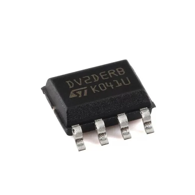
ST25DV04K-IER6S3 - 4Kbit Dynamic NFC/RFID Tag IC | STMicroelectronics
The ST25DV04K-IER6S3 is a dynamic NFC/RFID tag IC from STMicroelectronics, offering 4 Kbit of EEPROM memory with an I2C interface and an ISO 15693 / ISO 18000-3 Mode 1 compliant RF interface. It operates at 13.56 MHz and supports data rates up to 53 kbit/s in the RF interface, while the I2C interface supports up to 1 MHz. The device is housed in an SO-8 package (NXP-style) and is designed for applications requiring contactless data transfer and configuration, such as smart home devices, industrial equipment, and consumer electronics. Data verified as of 2026-08-05. What is a dynamic NFC/RFID tag IC? A dynamic NFC/RFID tag IC is a type of RFID transponder that combines a contactless RF interface with a wired interface (typically I2C) to allow a microcontroller to read and write the tag's memory both over the air and via the wired bus. This category sits within the broader hierarchy: NFC/RFID tag IC -> RFID transponder -> RFID/NFC integrated circuit -> wireless communication IC -> semiconductor. The dynamic nature means the tag can be updated in real time by the host MCU, enabling use cases like wireless configuration, data logging, and product authentication. Key features include 4 Kbit EEPROM organized in 128-byte pages, an I2C interface with a 1 MHz clock, an RF interface compliant with ISO 15693 and ISO 18000-3 Mode 1, a 64-bit unique identifier (UID), and an energy harvesting function that can power external circuits. The device supports a wide supply voltage range of 1.8V to 5.5V on the I2C side, and it includes an interrupt output to signal RF activity. The SO-8 package is compact and suitable for surface-mount assembly. Technically, the ST25DV04K-IER6S3 integrates an RF front-end with an analog-to-digital converter for energy harvesting, a state machine for protocol handling, and a memory controller for EEPROM access. The EEPROM is organized into 32 pages of 128 bits each, with a data retention of 10 years and an endurance of 1 million write cycles. The device supports both static and dynamic memory mapping, allowing the host to control which memory areas are accessible over RF. Typical applications include smart home devices (e.g., smart locks, thermostats), industrial equipment configuration, consumer electronics pairing (e.g., Bluetooth speakers, wearables), and medical device calibration. The energy harvesting feature enables battery-less operation for low-power sensors, and the I2C interface allows seamless integration with microcontrollers. When designing with this device, ensure proper antenna matching for the RF interface and place decoupling capacitors close to the VCC pin. The energy harvesting output should be buffered with a capacitor to provide stable power to external circuits. Also, consider the I2C address configuration via the RF field to avoid conflicts in multi-tag systems. This page synthesizes distributor pricing, drop-in alternatives, and practical design notes not found in the STMicroelectronics datasheet, providing a comprehensive resource for engineers evaluating the ST25DV04K-IER6S3.
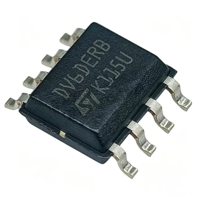
ST25DV64K-IER6S3 - 64Kbit Dynamic NFC/RFID Tag IC | STMicroelectronics
The ST25DV64K-IER6S3 is a 64-Kbit dynamic NFC/RFID tag IC from STMicroelectronics, designed for contactless data transfer and energy harvesting in IoT, smart home, and industrial applications. It operates at 13.56 MHz and supports ISO/IEC 15693 and ISO/IEC 18000-3 Mode 1 protocols, with a fast data transfer rate of up to 53 kbit/s. The device is housed in an SO-8 package and features an I2C interface for connection to a host microcontroller, enabling seamless integration into embedded systems. Data verified as of 2026-08-05. What is an NFC/RFID tag IC? An NFC/RFID tag IC is a passive integrated circuit that communicates with an NFC reader or RFID interrogator via radio frequency (RF) signals. It typically contains a memory array, an RF front-end, and a digital control unit. In the system hierarchy, an NFC tag IC falls under RFID transponders, which are part of the broader category of wireless communication devices. These ICs are essential for applications requiring wireless data exchange, such as access control, product authentication, and smart packaging, where they enable battery-less operation by harvesting energy from the reader's RF field. Key features of the ST25DV64K-IER6S3 include a 64-Kbit EEPROM memory organized in 256-byte pages, an I2C interface with a clock frequency of up to 1 MHz, and an energy harvesting function that can supply up to 1 mA to external circuits. The device supports a wide operating temperature range of -40°C to +85°C, making it suitable for industrial environments. It also features a configurable RF field detection output and an interrupt output for event-driven communication with the host MCU. Technically, the ST25DV64K-IER6S3 integrates an RF front-end with a high-sensitivity receiver, enabling reliable communication at distances up to 1.2 meters when used with a suitable antenna. The I2C interface allows the host to read and write the EEPROM memory, while the RF interface provides contactless access. The device includes a password protection mechanism for secure memory access, and its energy harvesting capability can power low-power sensors or charge a small capacitor for intermittent operation. Typical applications include smart home devices (e.g., smart locks, smart appliances), industrial asset tracking, medical device authentication, and consumer electronics pairing. The ST25DV64K-IER6S3 is particularly suited for applications requiring both contactless and wired communication, as it bridges the NFC world with traditional I2C-based systems. When designing with this device, ensure proper antenna matching and tuning to achieve optimal read range. The I2C pull-up resistors should be sized appropriately for the bus capacitance, and the energy harvesting output should be decoupled with a capacitor to stabilize the harvested voltage. This page synthesizes distributor pricing, drop-in alternatives, and practical design notes not found in the STMicroelectronics datasheet.

ST25R3916B - NFC Initiator with 1.4W Power | STMicroelectronics
The ST25R3916B is a highly integrated NFC initiator and card emulator from STMicroelectronics, designed for high-performance contactless communication. It supports ISO 14443A/B, ISO 15693, and FeliCa protocols, delivering up to 1.4W of output power for extended read range. The device operates from a 2.4V to 5.5V supply and is available in a 32-pin VFQFPN package. An NFC initiator is a device that actively generates an RF field to communicate with passive tags or cards. It is the core component in applications such as point-of-sale terminals, access control readers, and NFC-enabled consumer electronics. The ST25R3916B sits within the NFC reader IC family, which is part of the broader RFID and contactless communication IC category, ultimately falling under wireless communication semiconductors. Key features include a built-in high-efficiency power amplifier that delivers up to 1.4W, dynamic power control for optimal field strength, and advanced anti-collision algorithms for reliable multi-tag reading. The device also integrates a low-power card detection mode, making it suitable for battery-powered applications. Its high sensitivity and noise immunity ensure robust performance in noisy environments. The ST25R3916B employs a sophisticated analog front-end with automatic antenna tuning and calibration, simplifying PCB design and reducing component count. It supports both active and passive load modulation, enabling card emulation and peer-to-peer modes. The device includes a comprehensive set of registers for fine-tuning RF parameters, allowing designers to optimize performance for specific antenna configurations. Typical applications include payment terminals, access control systems, NFC-enabled smart locks, and industrial RFID readers. The high output power extends read range, while the low-power modes preserve battery life in portable devices. The device is also suitable for automotive key fobs and in-vehicle NFC modules. When designing with the ST25R3916B, careful attention must be paid to antenna matching and power supply decoupling. The device requires a clean supply voltage and proper grounding to achieve optimal RF performance. The SPI interface allows easy integration with microcontrollers, and the interrupt output simplifies event-driven firmware design.
ST25R3920B - NFC Reader IC, 13.56MHz, ISO 14443A/B | STMicroelectronics
The ST25R3920B is a high-performance NFC universal reader IC from STMicroelectronics, designed for 13.56 MHz contactless communication. It supports ISO 14443A/B, ISO 15693, and FeliCa protocols, making it a versatile solution for a wide range of NFC applications. The device operates from a 2.4V to 5.5V supply and features an integrated high-power transmitter with programmable output power up to 1.4W, enabling robust communication with passive tags and cards. An NFC reader IC is a specialized radio-frequency integrated circuit that manages the modulation, demodulation, and protocol handling required for near-field communication. It sits at the heart of contactless systems, bridging the digital host interface (typically SPI or I2C) and the analog RF front-end that drives the antenna. In the system hierarchy, the ST25R3920B functions as the physical layer and data-link layer controller, working alongside a host microcontroller (MCU) that runs the application stack. This separation allows designers to implement complex NFC functionality without deep RF expertise. Key features of the ST25R3920B include support for both active and passive peer-to-peer modes, an automatic antenna tuning system, and a low-power field detection mode that enables battery-efficient wake-up. The device also offers a high receiver sensitivity of -70 dBm, ensuring reliable reading of low-signal tags. Its integrated voltage regulator simplifies power supply design, and the SPI interface supports clock speeds up to 10 MHz for fast data transfer. From a technical architecture perspective, the ST25R3920B integrates a highly linear RF front-end with a 13.56 MHz carrier generation circuit, a multi-protocol framing engine, and a flexible FIFO buffer. The device uses a digital demodulator with adaptive filtering to handle various modulation depths and data rates, from 106 kbps to 848 kbps. Its automatic antenna tuning algorithm continuously adjusts the matching network to compensate for environmental detuning, maintaining optimal performance across different antenna designs and operating conditions. Typical applications include point-of-sale terminals, access control systems, NFC-enabled smart locks, and industrial asset tracking. In a POS terminal, the ST25R3920B provides the RF interface for contactless payment cards and mobile wallets, supporting the required EMVCo and NFC Forum compliance. For access control, its low-power field detection allows battery-operated door locks to wake up only when a card is presented, extending battery life. When designing with the ST25R3920B, careful attention must be paid to antenna matching and PCB layout to achieve optimal read range. The device's automatic tuning feature helps, but the antenna coil's inductance and Q-factor must be within the specified range. Additionally, proper decoupling and grounding are essential to minimize noise and ensure stable operation.
ST87M01-1000 - NB-IoT LTE Cat NB2 Module | STMicroelectronics
The STMicroelectronics ST87M01-1000 is an ultra-compact, low-power LTE Cat NB2 (NB-IoT) industrial cellular module supporting LTE FDD bands B1, B3, B5, B8, B20 and B28 for worldwide NB-IoT coverage, housed in an LGA package of 10.6 mm x 12.8 mm. It is the variant of the ST87M01 series without the integrated GNSS/Wi-Fi positioning capability, making it the lowest-power and most cost-effective choice for fixed or stationary IoT endpoints. An NB-IoT (Narrowband Internet of Things) module is a low-power wide-area (LPWAN) radio transceiver standardized by 3GPP for LTE Cat NB2. It sits within the broader hierarchy of cellular modules: transceiver -> cellular module -> wireless connectivity IC -> semiconductor device. NB-IoT prioritizes deep indoor penetration, ultra-low standby current and years of battery life over raw throughput, which suits metering, sensing and tracking infrastructure. Key features of the ST87M01 include fully programmable embedded processing, comprehensive worldwide band coverage on a single hardware SKU, and advanced security features per the STMicroelectronics product brief. The ultra-compact LGA footprint facilitates device miniaturization without compromising RF performance, and the industrial-grade design targets long deployment lifetimes. Architecturally, the ST87M01 series integrates the NB-IoT modem, baseband and RF front end into one module, exposing a standard LGA land pattern for direct PCB mounting. The 1.8 V supply domain simplifies power-tree design around common low-voltage batteries and regulators. ST describes it as the first all-in-one module family combining NB-IoT, GNSS and Wi-Fi positioning across its variants; the -1000 SKU provides the cellular function alone. Typical applications include smart electricity, gas and water metering, smart-city infrastructure such as street lighting and parking sensors, industrial condition monitoring, and asset-tracking endpoints where positioning is handled by another means. Design consideration: choose the -1000 variant when GNSS is not required, since the -1001 variant with GNSS capability costs more and consumes additional power; verify antenna keep-out and RF layout per the ST87M01 hardware design guidance. This page synthesizes distributor availability, drop-in family alternatives, and practical design notes not found in the manufacturer datasheet alone.

ST87M01-1001 - NB-IoT LTE Cat NB2 Module | STMicroelectronics
The STMicroelectronics ST87M01-1001 is an ultra-compact, low-power LTE Cat NB2 NB-IoT industrial cellular module supporting LTE FDD bands B1, B3, B5, B8, B20, and B28, delivering up to +23 dBm transmit output power in a 10.6 mm x 12.8 mm surface-mount LGA package with antenna not included. A cellular IoT module is a wireless communication subsystem that connects embedded devices to operator cellular networks. Within the power-management and connectivity hierarchy, NB-IoT (Narrowband IoT) sits under the LPWAN (Low-Power Wide-Area Network) family of 3GPP LTE standards, which in turn belong to the broader categories of wireless transceivers, RF modules, and industrial IoT communication ICs. NB-IoT modules are optimized for low data rates, deep indoor coverage, and multi-year battery life rather than throughput. Key features of the ST87M01-1001 include comprehensive worldwide band coverage across six LTE FDD bands, ultra-low power consumption of less than 2 uA in low-power mode for multi-year battery operation, and fully programmable architecture allowing customer applications to run on-module. It is a certified LTE Cat NB2 design per the 3GPP release on which it is based, and STMicroelectronics guarantees 15 years of availability, a critical factor for industrial product lifecycles. Technically, the ST87M01 series integrates the cellular modem with advanced security features and industrial-grade design. The -1001 variant provides NB-IoT connectivity plus an extra ADC, while the -1301 and -2301 variants add GNSS and Wi-Fi positioning for combined cellular-plus-location designs. The industrial operating range of -40 C to +85 C supports harsh deployments such as outdoor metering and cold-chain tracking. Typical applications include smart utility metering (electricity, gas, water), asset tracking and telematics, smart city infrastructure such as parking and streetlight control, and industrial sensors on NB-IoT networks. The 868.95 MHz reference in listings relates to adjacent sub-GHz positioning options; the cellular path uses the licensed LTE FDD bands listed above. Design consideration: NB-IoT coverage and SIM/eSIM data plans vary by country and operator, so verify operator NB-IoT support early in the project. Antenna selection and RF layout are also critical because no antenna is included. This page synthesizes distributor pricing, same-family drop-in alternatives, and practical design notes not found in the STMicroelectronics datasheet.
ST87M01-1100 - NB-IoT Module with GNSS | STMicroelectronics
The STMicroelectronics ST87M01-1100 is an ultra-compact, low-power LTE Cat NB2 (NB-IoT) industrial module with integrated GNSS/Wi-Fi positioning, certified by Anatel for Brazil and supporting LTE FDD bands B1, B3, B5, B8, B20, and B28. An NB-IoT module is a type of cellular wireless module within the broader family of LPWAN (Low-Power Wide-Area Network) connectivity devices. NB-IoT operates on licensed LTE spectrum and provides deep indoor penetration and long battery life, making it a key building block of power management-aware, battery-operated industrial IoT systems alongside sensors, microcontrollers, and cellular infrastructure. Key features of the ST87M01 family include its all-in-one integration of NB-IoT cellular connectivity, GNSS (GPS/Galileo) satellite positioning, and Wi-Fi 802.11b-based positioning in a single ultra-compact surface-mount package. This eliminates the need for a separate positioning module, reducing BOM count, board area, and integration effort. The family is described by ST as fully programmable, high-performance, and certified, with worldwide band coverage and advanced security features. Technically, the ST87M01 series is an LTE Cat NB2 device, the evolution of 3GPP NB-IoT supporting higher peak data rates than Cat NB1. ST guarantees 15 years of availability for the ST87M01 platform, which is a critical procurement criterion for industrial products with long service lifetimes. Security features are embedded per the manufacturer product page, and the module supports both classic SIM and externally connected eSIM. Typical applications include smart metering, smart street lighting, asset tracking, livestock and agriculture monitoring, and other smart-city verticals - especially in Brazil and other regions using the B1/B3/B5/B8/B20/B28 band set covered by this -1100 region variant. Design consideration: choose the region-specific variant that matches your deployment market and operator certification requirements; ST explicitly directs users to confirm NB-IoT coverage and suitable SIM data plans with their operator before finalizing the design. This page synthesizes manufacturer data, region-variant guidance, drop-in family alternatives, and practical design notes not found on distributor listing pages.
ST87M01-1101 - NB-IoT Module with GNSS | STMicroelectronics
The STMicroelectronics ST87M01-1101 is an ultra-compact, low-power LTE Cat NB2 (NB-IoT) industrial module with integrated GNSS (GPS/Galileo) and Wi-Fi positioning capability plus an extra ADC, supporting LTE FDD frequency bands B1, B3, B5, B8, B20, and B28 for comprehensive worldwide band coverage. An NB-IoT module is a type of cellular LPWAN (Low Power Wide Area Network) transceiver subsystem that sits within the broader hierarchy of wireless connectivity solutions: cellular module, RF transceiver, RF & wireless component. NB-IoT operates on licensed spectrum with deep indoor penetration and carrier-grade security, making it distinct from unlicensed-technologies such as LoRa or Sigfox. Modules like the ST87M01 series integrate the baseband modem, RF front end, power management, and optional positioning engines into a single certified surface-mount unit. The ST87M01-1101 differentiates itself as one of the first all-in-one modules to combine NB-IoT connectivity, GNSS, and Wi-Fi positioning in a single package, eliminating the need for a separate positioning module in asset-tracking designs. Its LTE Cat NB2 compliance enables deployment on 3GPP Release 14 NB-IoT networks, and ST highlights advanced security features and full programmability for industrial applications. The -1101 variant adds GNSS and Wi-Fi positioning plus the additional ADC, and is Anatel-certified for the Brazilian market alongside the ST87M01-1100. Architecturally, the module series is built for ultra-low power consumption, targeting battery-powered endpoints where multi-year battery life is a design requirement. The integrated GNSS receiver supports GPS and Galileo constellations, while the Wi-Fi sniffing capability provides urban positioning where satellite visibility is poor, and the auxiliary ADC allows direct connection of analog sensors without an external converter. Typical applications include asset tracking, smart metering, smart city infrastructure, and battery-powered industrial IoT sensors. In asset trackers, the combination of NB-IoT and GNSS/Wi-Fi positioning in one module reduces BOM count and board area; in metering, the ultra-low-power profile extends battery service intervals. When designing with the ST87M01-1101, verify antenna selection and RF layout against the ST evaluation kit reference design, and confirm the region-specific certification variant matches your target market, since ST ships distinct MPNs for North America (ST87M01-2001/-2301), Brazil (ST87M01-1000/-1100/-1101), and other regions. This page synthesizes distributor listings, the manufacturer datasheet, family-variant cross-references, and pricing context not consolidated in the ST datasheet alone.
ST87M01-2001 - NB-IoT LTE Cat NB2 Module | STMicroelectronics
The STMicroelectronics ST87M01-2001 is an ultra-compact, low-power LTE Cat NB2 NB-IoT industrial cellular module from the ST87M01 family, purpose-built for North American markets (USA and Canada regional certification) with Anatel-certified siblings covering Brazil. The -2001 variant provides NB-IoT connectivity only, allowing designers to lower the bill of materials when positioning is not required, while family members such as the ST87M01-2301 add GNSS and Wi-Fi positioning in the same footprint. An NB-IoT (Narrowband Internet of Things) module is a low-power wide-area network (LPWAN) cellular transceiver that operates within licensed spectrum on LTE Category NB2. Within the wireless connectivity hierarchy, NB-IoT modules sit alongside LTE-M and LoRa devices as long-range, low-throughput radios optimized for battery-powered telemetry, smart metering, and asset tracking. The ST87M01 family is positioned as a certified industrial-grade option with multi-band worldwide coverage. Key features of the ST87M01 series include LTE Cat NB2 operation, comprehensive worldwide band coverage, advanced security features, ultra-low power consumption for battery-operated designs, and an ultra-compact surface-mount form factor. According to STMicroelectronics, the family is fully programmable, and ST guarantees 15 years of availability, a critical commitment for industrial product lifecycles. The module integrates the cellular protocol stack in firmware (maintained via the STSW-ST87M01 firmware bundle) and connects to host systems over serial interfaces, with support for both classic SIM cards and externally connected eSIM. The family is programmable, enabling application-level processing on-module rather than on a separate host MCU in some designs. Typical applications include smart utility metering, asset tracking, industrial telemetry, smart city infrastructure, and battery-powered IoT sensor nodes deployed on North American NB-IoT networks. The -2001 variant is the right choice where cellular connectivity alone suffices. Design considerations include verifying operator NB-IoT coverage and SIM data plans for the deployment region, providing an adequate power supply for RF transmit bursts, and following the STDES-ST87M01IGN reference design for antenna and layout guidance. This page synthesizes datasheet information, family cross-references, drop-in alternatives, and practical design notes not found in the manufacturer datasheet alone.
ST87M01-2301 NB-IoT + GNSS/Wi-Fi Module | STMicroelectronics
The STMicroelectronics ST87M01-2301 is an ultra-compact, low-power LTE Cat NB2 NB-IoT industrial module with integrated GNSS and Wi-Fi positioning plus an extra ADC, supporting LTE FDD frequency bands B2, B4, B5, B12, B13, B66 and B85 for North American networks. A cellular module is a self-contained wireless subassembly that integrates an LTE modem baseband, RF transceiver, front-end, power management and protocol stack on a single surface-mount land pattern, connecting a host microcontroller to operator networks through a simple UART or USB interface. Within the IoT connectivity hierarchy, NB-IoT (Narrowband IoT, standardized by 3GPP as LTE Cat NB2) sits alongside LTE-M as a licensed-spectrum LPWAN technology optimized for low data rates, deep indoor coverage and multi-year battery life. Key differentiating features of the ST87M01-2301 include its all-in-one integration of NB-IoT cellular, GNSS satellite positioning and Wi-Fi positioning - which ST describes as the first such combination in the industry - together with advanced security features and full programmability of the module firmware. The module series is described by STMicroelectronics as high-performance, fully programmable, ultra-compact and low-power, certified for LTE Cat NB2 operation with comprehensive worldwide band coverage. The -2301 variant is region-targeted for the USA and Canada and is certified for those markets, with companion Anatel-certified variants (-1100/-1101) available for Brazil. Typical applications include asset tracking (where GNSS and Wi-Fi positioning remove the need for a separate positioning IC), smart metering, smart-city infrastructure and battery-powered industrial sensors - use cases showcased in the STEVAL-NBIOTV1 evaluation platform and the STDES-ST87M01IGN 2-layer FR4 reference design. Design considerations: NB-IoT coverage and operator support must be confirmed per country, and SIM selection (eSIM or classic SIM, both supported) affects the data plan; RF layout should follow the STDES-ST87M01IGN reference design for antenna matching and power integrity. This page synthesizes datasheet data, family-variant drop-in alternatives, evaluation-tool pairings and pricing references not consolidated in the manufacturer datasheet alone.
STA8089FGATR - GPS/Galileo/GLONASS Receiver IC | STMicroelectronics
The STA8089FGATR is a high-performance, single-chip GPS/Galileo/GLONASS receiver IC from STMicroelectronics, designed for automotive and industrial positioning applications. It integrates a complete RF front-end, baseband processor, and ARM9 CPU core in a compact VFQFPN-56 package, enabling accurate positioning with low power consumption. The device supports multiple satellite constellations simultaneously, providing robust and reliable navigation in challenging environments. A GNSS receiver is a radio-frequency (RF) device that captures signals from global navigation satellite systems (GNSS) such as GPS, Galileo, GLONASS, and BeiDou, and processes them to determine the receiver's precise position, velocity, and time. The STA8089FGATR belongs to the category of GNSS receivers, which are a subset of RF and wireless modules, and ultimately fall under the broader category of electronic components used in navigation and timing systems. This hierarchy helps engineers understand its role in system design: GNSS receiver -> RF module -> wireless communication -> electronic component. Key features of the STA8089FGATR include support for GPS L1 C/A, Galileo E1, and GLONASS L1 signals, a high-sensitivity RF front-end with -162 dBm tracking sensitivity, and an integrated ARM9 processor running at 166 MHz. The device offers a low power consumption of 45 mA in continuous tracking mode, making it suitable for battery-powered and automotive applications. It also includes a built-in 3.3V LDO regulator, a 1.8V core supply, and multiple UART, SPI, and I2C interfaces for host communication. Technically, the STA8089FGATR employs a single-chip architecture that combines the RF tuner, baseband correlator, and navigation processor, reducing external component count and system cost. The device supports assisted GPS (A-GPS) and ephemeris prediction for faster time-to-first-fix (TTFF), and includes a real-time clock (RTC) for power-saving modes. Its firmware is upgradeable via the serial interface, allowing for future feature enhancements. Typical applications include automotive navigation systems, fleet management, personal tracking devices, and industrial timing synchronization. The device's multi-constellation support ensures reliable positioning in urban canyons and dense foliage where single-constellation receivers may fail. When designing with the STA8089FGATR, ensure proper RF layout with a 50-ohm impedance-controlled antenna trace and adequate decoupling on all power pins. The VFQFPN-56 package requires a thermal pad connection to ground for optimal heat dissipation and electrical performance.
STA8089GADTR - GPS/Galileo/GLONASS Receiver IC | STMicroelectronics
The STA8089GADTR is a high-performance, single-chip GPS/Galileo/GLONASS receiver IC from STMicroelectronics, designed for automotive and industrial positioning applications. It integrates a complete RF front-end, baseband processor, and ARM9 core in a compact VFQFPN-56 package, delivering accurate positioning with low power consumption. The device supports multiple satellite constellations simultaneously, ensuring robust performance in urban canyons and challenging environments. A GNSS receiver is a specialized radio receiver that processes signals from satellite navigation systems to determine precise geographic position, velocity, and time. The STA8089GADTR belongs to the category of satellite navigation ICs, which are essential components in modern navigation systems, telematics, and location-based services. These ICs convert raw satellite signals into usable position data, often integrating RF, baseband, and processing functions on a single chip to reduce system cost and complexity. Key features of the STA8089GADTR include support for GPS, Galileo, and GLONASS constellations, a high-sensitivity RF front-end with -162 dBm tracking sensitivity, and an embedded ARM9 processor for application processing. The device offers a low power consumption of 45 mA in continuous tracking mode, making it suitable for battery-powered devices. It also includes a comprehensive set of interfaces, including UART, SPI, I2C, and USB, enabling flexible system integration. The STA8089GADTR is built on STMicroelectronics' advanced CMOS process technology, integrating the RF front-end, baseband, and application processor on a single die. This integration reduces external component count and simplifies PCB design. The device supports assisted GPS (A-GPS) for faster time-to-first-fix (TTFF) in weak signal environments, and includes an integrated LNA for improved sensitivity. The ARM9 core runs the navigation firmware and can be used for custom application code, providing a complete GNSS solution. Typical applications include automotive navigation systems, fleet management, personal tracking devices, and industrial IoT devices requiring precise location data. The STA8089GADTR is also suitable for telematics and emergency call (eCall) systems, where reliable positioning is critical. Its multi-constellation support ensures continuous operation even when one satellite system is unavailable. When designing with the STA8089GADTR, ensure proper RF layout with a clean ground plane and adequate decoupling on the power supply pins. The device requires a 26 MHz reference crystal and a 32.768 kHz RTC crystal for accurate timekeeping. Follow the manufacturer's reference design for optimal antenna matching and RF performance.