RF و بیسیم
زیردستهها
محصولات (700+)

STA8089GATR - GPS/Galileo/GLONASS Receiver IC | STMicroelectronics
The STA8089GATR is a high-performance, single-chip GPS/Galileo/GLONASS receiver IC from STMicroelectronics, designed for automotive and industrial positioning applications. It integrates a complete RF front-end, baseband processor, and ARM9 CPU core in a compact VFQFPN-56 package, enabling accurate and reliable global navigation satellite system (GNSS) functionality. The device supports concurrent reception of GPS, Galileo, GLONASS, and QZSS signals, providing enhanced positioning accuracy and availability in challenging environments. A GNSS receiver IC is a specialized system-on-chip (SoC) that captures satellite signals, downconverts them to an intermediate frequency, and processes them to compute position, velocity, and time. The STA8089GATR belongs to the GNSS receiver category, which is a subset of RF and wireless communication ICs. It combines an RF tuner, digital baseband processor, and application processor, making it a complete solution for location-based services. Key features of the STA8089GATR include a 32-channel tracking engine, -162 dBm tracking sensitivity, and a low power consumption of 45 mA in continuous tracking mode. It supports both active and passive antennas, with an integrated LNA and SAW filter interface. The device also features a built-in ARM9 processor running at 96 MHz, which can execute user applications and handle communication protocols. Its wide operating voltage range of 1.8V to 3.6V and industrial temperature range of -40°C to +85°C make it suitable for harsh automotive environments. The STA8089GATR employs advanced RF CMOS technology, achieving high integration and low power consumption. Its architecture includes a direct-conversion receiver, which simplifies the RF front-end and reduces external component count. The baseband processor uses a hardware correlator for efficient satellite signal acquisition and tracking, while the ARM9 core handles navigation algorithms and user interface tasks. This dual-core design enables real-time positioning with minimal latency. Typical applications include automotive navigation systems, fleet management, telematics, and portable navigation devices (PNDs). The device's high sensitivity and multi-constellation support ensure reliable positioning in urban canyons and under tree cover. Its low power consumption extends battery life in portable devices, while the industrial temperature range supports under-hood automotive installations. When designing with the STA8089GATR, ensure proper RF layout with a 50-ohm impedance-controlled trace to the antenna, and place decoupling capacitors close to the power pins. The device requires a clean power supply and a stable reference clock (26 MHz TCXO) for optimal performance. Refer to the STMicroelectronics application note AN4650 for detailed design guidelines.
STA8090GATR - GPS/Galileo/Glonass Receiver IC | STMicroelectronics
The STA8090GATR is a high-performance, multi-constellation GNSS receiver IC from STMicroelectronics, designed for automotive and industrial positioning applications. It supports GPS, Galileo, GLONASS, and BeiDou constellations, providing accurate and reliable positioning data. The device integrates an RF front-end, baseband processor, and power management unit in a compact VFQFPN-56 package, making it ideal for space-constrained designs. A GNSS receiver is a specialized radio receiver that processes signals from satellite navigation systems to determine precise geographic position, velocity, and time. It is a critical component in the broader positioning and navigation system hierarchy, which includes antennas, RF front-ends, baseband processors, and application processors. The STA8090GATR combines these functions into a single chip, reducing system complexity and power consumption. Key features of the STA8090GATR include support for concurrent reception of GPS, Galileo, GLONASS, and BeiDou signals, a high-sensitivity RF front-end with -162 dBm tracking sensitivity, and an integrated ARM-based baseband processor. It also features a low-power mode with typical current consumption of 25 mA during continuous tracking, and a standby current of 10 uA. The device operates from a 1.8V supply and includes an integrated LDO for internal voltage regulation. The STA8090GATR utilizes advanced CMOS technology and a multi-core architecture to handle complex signal processing algorithms, including multipath mitigation and interference rejection. Its high sensitivity and fast time-to-first-fix (TTFF) make it suitable for demanding environments such as urban canyons and dense foliage. The device also supports assisted GPS (A-GPS) and ephemeris prediction for faster fixes. Typical applications include automotive navigation systems, fleet management, telematics, and portable navigation devices. The STA8090GATR is also used in IoT devices requiring location tracking, such as asset trackers and wearables. Its low power consumption and small footprint make it an excellent choice for battery-powered applications. When designing with the STA8090GATR, ensure proper antenna matching and grounding for optimal RF performance. The device requires a clean 1.8V supply and careful PCB layout to minimize noise and interference. Refer to the STMicroelectronics application notes for detailed design guidelines.
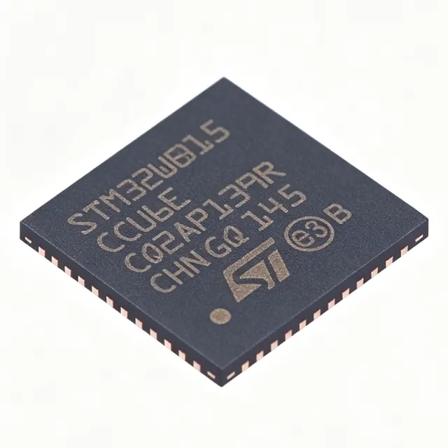
STM32WB15CCU6 - 2.4GHz BLE 5.2 Wireless MCU, 320KB Flash | STMicroelectronics
The STMicroelectronics STM32WB15CCU6 is a dual-core wireless microcontroller integrating a 64 MHz Arm Cortex-M4 application processor and a 32 MHz Arm Cortex-M0+ radio processor, designed for Bluetooth Low Energy 5.2 applications. It features 320 KB of flash memory and 48 KB of SRAM, housed in a 48-pin UFQFPN (UFQFPN-48) package with dimensions of 7x7 mm. The device supports a supply voltage range of 1.71V to 3.6V and operates over a temperature range of -40°C to +105°C, making it suitable for industrial and consumer IoT applications. A wireless microcontroller (MCU) is a system-on-chip that integrates a general-purpose microcontroller core with a radio transceiver, enabling wireless communication protocols such as Bluetooth Low Energy, Zigbee, or proprietary sub-GHz protocols. In the system hierarchy, a wireless MCU sits above a standalone MCU and below a full application processor, providing a balance of processing capability, low power consumption, and wireless connectivity. The STM32WB15CCU6 specifically targets Bluetooth Low Energy 5.2, offering a complete solution for connected devices without requiring an external radio chip. Key features of the STM32WB15CCU6 include a 2.4 GHz radio supporting Bluetooth Low Energy 5.2 with a transmit power of up to +6 dBm and a receiver sensitivity of -96 dBm, ensuring robust wireless links. The dual-core architecture allows the Cortex-M0+ to handle the radio stack independently, freeing the Cortex-M4 for application tasks, which improves real-time performance and reduces power consumption. The device also includes a rich set of peripherals, including multiple UART, SPI, I2C interfaces, a 12-bit ADC, and a random number generator, providing flexibility for various sensor and control applications. From a technical depth perspective, the STM32WB15CCU6 leverages ST's advanced 40nm process technology, enabling low power consumption with multiple low-power modes, including a standby mode with a current consumption of only 1.6 µA. The radio architecture includes a dedicated hardware encryption engine supporting AES-128, AES-256, and other algorithms, ensuring secure wireless communication. The device also features a true random number generator (TRNG) and a unique 96-bit ID, enhancing security for IoT applications. Typical applications include smart home devices such as smart locks, sensors, and lighting controls, as well as healthcare wearables, industrial wireless sensor networks, and asset tracking systems. The STM32WB15CCU6's low power consumption and robust wireless performance make it ideal for battery-powered devices that require long operational lifetimes. When designing with this device, ensure proper antenna matching and PCB layout for the 2.4 GHz radio to achieve optimal range and reliability. The device requires a 32.768 kHz crystal for the low-power RTC and a 32 MHz crystal for the radio, and careful attention to power supply decoupling is essential to minimize noise and ensure stable operation.
STM32WB55RGV6 - Dual-Core BLE 5.3 MCU 1MB Flash | STMicroelectronics
The STMicroelectronics STM32WB55RGV6 is an ultra-low-power multiprotocol wireless microcontroller with a dual-core architecture - an Arm Cortex-M4 with FPU running at 64 MHz for the application and an Arm Cortex-M0+ running at 32 MHz dedicated to the radio stack - with 1 Mbyte of Flash memory, integrated Bluetooth Low Energy 5.3/5.4-compliant and IEEE 802.15.4-2011 radio covering 2.405 GHz to 2.48 GHz, housed in a 68-pin VFQFPN exposed-pad package. A wireless MCU is a microcontroller that integrates both a processing core and a radio transceiver on a single die, sitting at the intersection of the microcontroller and RF transceiver product categories within the broader wireless-connectivity semiconductor hierarchy. By partitioning the real-time radio stack onto the Cortex-M0+ and the user application onto the Cortex-M4, the STM32WB55 family guarantees RF protocol timing independence from application load - a key architectural advantage over single-core BLE MCUs. Key features include 1 MB of Flash and 256 KB of SRAM for application and stack storage, support for Bluetooth 5.3, Thread, and Zigbee protocols on the same silicon, a rich peripheral set (USB 2.0 full-speed device, USART, SPI, I2C, I2S, Quad-SPI, 12-bit ADC, comparators, touch sensing), and ultra-low-power modes with down to a few microamps in Stop 2 with RAM retention. The integrated balun and output power up to +6 dBm (as per family datasheet range) simplify RF front-end design. The dual-core radio architecture offloads BLE/802.15.4 stacks from the application core, so deterministic real-time behavior, security via the Cortex-M0+ trust boundary, and OTA firmware update capability are maintained even under heavy application processing. The 68-pin VFQFPN-EP (7x7 mm class) package provides a good GPIO count for sensor hubs and HMI. Typical applications include smart-home sensors and lighting (Thread/Zigbee), Bluetooth LE beacons and wearables, industrial wireless nodes, and medical monitoring devices. Design consideration: RF layout requires a 50-ohm match to the antenna and solid ground planes on the exposed pad; verify the exact radio output-power and sensitivity figures against the official STM32WB55xx datasheet. This page synthesizes distributor pricing, drop-in alternatives, comparison tables, and design notes not found in the manufacturer datasheet.

STM32WB55VEQ6 - 2.4GHz Dual-Core Wireless MCU | STMicroelectronics
The STMicroelectronics STM32WB55VEQ6 is a dual-core wireless microcontroller that integrates a 64 MHz Arm Cortex-M4 application processor with a 32 MHz Arm Cortex-M0+ dedicated to radio processing, enabling concurrent execution of application code and Bluetooth Low Energy (BLE) 5.0, Zigbee 3.0, and OpenThread stacks. It is housed in a 129-ball UFBGA (VQFN-129) package, offering a compact footprint for space-constrained IoT devices. A wireless microcontroller (MCU) is a system-on-chip that combines a general-purpose processor core with a radio transceiver, allowing embedded systems to communicate wirelessly. The STM32WB55VEQ6 belongs to the STM32WB series, which is part of the broader STM32 family of 32-bit Arm Cortex-M microcontrollers. This hierarchy places it within the categories of wireless MCU -> microcontroller -> embedded processor -> semiconductor, providing a clear taxonomy for engineers selecting components for IoT applications. Key features include 1 Mbyte of flash memory and 256 Kbytes of SRAM, providing ample storage for complex application firmware and protocol stacks. The device supports a wide supply voltage range of 1.71V to 3.6V, making it suitable for battery-powered applications. It also integrates a rich set of analog peripherals, including a 12-bit ADC, operational amplifiers, and comparators, as well as digital interfaces such as SPI, I2C, USART, and USB 2.0 FS. The radio supports BLE 5.0 with a data rate of up to 2 Mbps, Zigbee 3.0, and OpenThread, with a typical sensitivity of -96 dBm for BLE. The dual-core architecture allows the Cortex-M0+ to handle all real-time radio protocol processing, while the Cortex-M4 runs the application code, ensuring deterministic wireless performance without burdening the main processor. The device also features a hardware cryptographic accelerator (AES, RSA, ECC) and a true random number generator (TRNG) for secure communication, which is critical for IoT security. Typical applications include smart home devices (e.g., smart locks, sensors, lighting), industrial wireless sensor networks, healthcare wearables, and asset tracking systems. The low-power modes, including Sleep, Stop, and Standby, with current consumption as low as 1.62 uA in Standby mode, extend battery life in portable applications. When designing with this device, ensure proper antenna matching and RF layout to achieve optimal radio performance. The device requires a 32.768 kHz crystal for the RTC and a 32 MHz crystal for the radio, and careful PCB design is essential to minimize interference between the RF section and digital circuitry.

STM32WBA52CEU6 - Arm Cortex-M33 BLE 5.4 MCU | STMicroelectronics
The STM32WBA52CEU6 is a 32-bit Arm Cortex-M33 microcontroller from STMicroelectronics, featuring a 100 MHz core with TrustZone, DSP instructions, and a floating-point unit (FPU). It integrates a 2.4 GHz radio supporting Bluetooth Low Energy (BLE) 5.4, making it ideal for secure IoT and wireless applications. The device comes in a UFQFPN-48 package (7x7 mm) and operates over a supply voltage range of 1.71V to 3.6V. A microcontroller (MCU) is a compact integrated circuit designed to govern a specific operation in an embedded system. It contains a processor core, memory, and programmable input/output peripherals. The STM32WBA52CEU6 belongs to the STM32WBA series, which is part of the broader STM32 family of 32-bit microcontrollers. This series is optimized for wireless connectivity, combining the Arm Cortex-M33 core with a radio transceiver, enabling secure and low-power communication in IoT devices. Key features include 512 KB of flash memory and 128 KB of SRAM, a rich set of analog and digital peripherals, and advanced security features such as TrustZone, secure boot, and hardware cryptographic accelerators. The BLE 5.4 radio supports long-range, high-throughput, and advertising extensions, with a link budget of up to 105 dB. The device also includes a 12-bit ADC, multiple timers, and communication interfaces like SPI, I2C, USART, and USB. The STM32WBA52CEU6 is built on a low-power process technology, offering multiple low-power modes including Sleep, Stop, and Standby, with typical current consumption as low as 2.2 uA in Standby mode with RTC. The TrustZone technology provides hardware-enforced isolation for secure code execution, making it suitable for applications requiring robust security, such as secure payment, authentication, and firmware protection. Typical applications include smart home devices, industrial sensors, medical wearables, and asset tracking. The integrated BLE radio and security features make it a strong choice for IoT edge nodes that need secure wireless communication. The device supports over-the-air (OTA) firmware updates, enabling remote maintenance and feature updates. When designing with this MCU, ensure proper antenna matching for the BLE radio and follow the layout guidelines in the datasheet to minimize RF interference. The supply voltage should be decoupled with a 100 nF capacitor close to each VDD pin, and the VDDA pin should have a dedicated 1 uF capacitor for analog performance.
STM32WBA55RGV6 - 100MHz Cortex-M33 BLE 5.4 MCU | STMicroelectronics
The STMicroelectronics STM32WBA55RGV6 is a wireless microcontroller (MCU) integrating an Arm Cortex-M33 core running at up to 100 MHz with a 2.4 GHz radio supporting Bluetooth Low Energy (BLE) 5.4, Zigbee, Thread, and proprietary protocols. It is housed in a 28-pin VFQFPN (VG) package with a 4x4 mm footprint, offering a compact solution for connected embedded applications. A wireless MCU is a system-on-chip that combines a general-purpose microcontroller with a radio transceiver, enabling wireless communication in embedded systems. The STM32WBA55RGV6 belongs to the STM32WBA family, which is part of the broader STM32 microcontroller portfolio from STMicroelectronics. This family is designed for low-power, secure, and connected applications, bridging the gap between traditional MCUs and dedicated wireless SoCs. Key features include 512 KB of flash memory and 128 KB of SRAM, providing ample space for application code and data. The device supports a wide supply voltage range of 1.71V to 3.6V, making it suitable for battery-powered designs. It integrates a rich set of peripherals, including multiple UART, SPI, I2C, ADC, timers, and GPIOs, along with advanced security features such as TrustZone, secure boot, and hardware cryptographic accelerators (AES, RSA, ECC). The radio achieves a sensitivity of -96 dBm for BLE, ensuring reliable communication. The STM32WBA55RGV6 is built on a low-power process technology, with multiple low-power modes (Sleep, Stop, Standby) to minimize energy consumption. The Arm Cortex-M33 core with TrustZone provides hardware-enforced isolation for secure applications, while the radio supports concurrent multi-protocol operation, enabling seamless switching between BLE and Zigbee/Thread. This makes it ideal for IoT nodes, smart home devices, and industrial sensors. Typical applications include smart home automation (e.g., smart locks, sensors), wearable health monitors, industrial wireless sensor networks, and asset tracking. The device's low power consumption and robust security features make it well-suited for battery-operated devices that require secure wireless connectivity. When designing with this device, pay attention to antenna matching and RF layout to achieve optimal radio performance. The device requires a 32 MHz crystal for the radio and a 32.768 kHz crystal for low-power timing. Proper decoupling of the supply pins and a clean ground plane are essential for reliable operation.

STM32WBA5MMGH6TR - Cortex-M33 BLE 5.4/Thread/Zigbee Module | ST
The STMicroelectronics STM32WBA5MMGH6TR is an ultra-low-power Arm Cortex-M33 TrustZone MCU module integrating Bluetooth LE 5.4, IEEE 802.15.4 (Thread/Zigbee) radio, and 1 Mbyte of Flash memory in a 76-pin LGA module (8 x 12.5 mm). The module runs the Cortex-M33 core at up to 100 MHz with TrustZone security extensions and is designed for connected devices that require multi-protocol 2.4 GHz wireless connectivity without a discrete radio stack on the host MCU. A wireless MCU module combines an application processor, memory, peripherals, and a certified RF subsystem in a single surface-mount land-grid package. In the broader hierarchy, the STM32WBA5MMGH6TR sits under MCU module -> Wireless SoC -> short-range transceiver, where the integrated Cortex-M33 host manages both application code and the radio link layer. This integration eliminates the need for an external radio co-processor, reduces BOM count, and shortens certification time for end products targeting Bluetooth LE, Thread, Zigbee, or Matter ecosystems. Key features of the STM32WBA5MMGH6TR include 1 Mbyte of Flash, up to 100 MHz Cortex-M33 core with TrustZone, Bluetooth LE 5.4 certification-ready radio, integrated 2.4 GHz antenna matching network, and support for Thread/Zigbee via 802.15.4. The module exposes GPIO, I2C, SPI, USART, and ADC peripherals on the LGA pads. Security is enhanced by TrustZone isolation, secure boot, and hardware cryptographic accelerators. Ultra-low-power operation targets always-on battery-powered IoT endpoints. Architecturally, the device pairs an applications Cortex-M33 core with a dedicated 2.4 GHz radio subsystem. The radio chain supports BLE 5.4 (Coded PHY/LE 2M), IEEE 802.15.4 O-QPSK, and proprietary modes. RF matching, balun, and antenna tuning are integrated, removing the need for external RF components. The 76-pin LGA exposes digital I/O, debug (SWD/JTAG), and RF test access, enabling both prototype bring-up and production assembly via standard SMT lines. Typical applications include Bluetooth LE lighting, Matter-over-Thread smart-home devices, Zigbee sensors, BLE wearables, industrial wireless sensor nodes, and asset-tracking beacons. The combination of Cortex-M33 headroom with multi-protocol 2.4 GHz radio makes it well suited to gateways bridging Thread/Zigbee and BLE ecosystems. When designing in the STM32WBA5MMGH6TR, follow ST's recommended PCB footprint and keep the antenna keep-out region clear of copper and plastic. Provide adequate decoupling near the supply pads and verify regulatory compliance for the end device in your target region. This page synthesizes distributor pricing, drop-in STM32WBA module alternatives, and practical PCB/RF layout guidance not consolidated in the ST datasheet alone.

STM32WBA62CGU6 - BLE 5.4 Multiprotocol MCU 100MHz | ST
The STMicroelectronics STM32WBA62CGU6 is a multiprotocol wireless 32-bit microcontroller with an Arm Cortex-M33 core with TrustZone and FPU running at up to 100 MHz, 2 Mbytes of flash memory and 512 Kbytes of RAM, integrating a 2.4 GHz radio compliant with Bluetooth LE 5.4 and IEEE 802.15.4-2015, housed in a 48-pin UFQFN package with exposed pad. A wireless MCU is a microcontroller that combines a general-purpose processor core with an integrated radio transceiver, allowing a single chip to run both application firmware and a wireless protocol stack. Within the power-management hierarchy, the STM32WBA6 belongs to the STM32 wireless MCU family (STM32WBA series -> STM32 32-bit Arm Cortex MCUs -> microcontrollers -> embedded processors), positioned as the high-end member offering large flash memory for concurrent multi-protocol stacks. Key differentiating features include Bluetooth Low Energy 5.4 and IEEE 802.15.4-2015 radio compliance supporting Zigbee, Thread, and Matter protocols with simultaneous multi-protocol operation, up to 2 Mbytes of flash and 512 Kbytes of RAM for large concurrent stacks, up to 86 GPIOs, and USB high-speed support for advanced connectivity. The device is built on a 40 nm process technology optimized for ultra-low-power operation and is compliant with RED and US security standards. Architecturally, the Cortex-M33 with Arm TrustZone provides hardware-enforced security isolation, essential for Matter certification and secure over-the-air updates. The FPU accelerates signal processing for sensor fusion and audio applications. ST supports development through the STM32CubeWBA firmware package with HAL drivers, BLE, Zigbee, Thread, and Matter middleware. Typical applications include smart-home Matter/Zigbee/Thread hubs, Bluetooth LE sensors and lighting, industrial wireless nodes, and connected building devices where large flash enables dual-image OTA and multi-stack coexistence. Design consideration: multi-protocol concurrent operation increases RAM and flash footprint; budget at least 512 Kbytes RAM headroom and follow the STM32CubeWBA reference designs for RF matching and antenna layout. This page synthesizes distributor inventory data, the manufacturer datasheet and migration application note AN6159, drop-in family alternatives, and practical design guidance not found on any single distributor page.
STM32WBA62PII6 - 100MHz Cortex-M33 BLE MCU | ST | IoT
The STMicroelectronics STM32WBA62PII6 is an ultra-low-power multiprotocol wireless microcontroller built on an Arm Cortex-M33 core with TrustZone and FPU, running at 100 MHz with 2 Mbytes of Flash memory, integrating a Bluetooth Low Energy 5.4 and IEEE 802.15.4 radio in a 121-ball UFBGA package. A wireless MCU (microcontroller unit) combines a general-purpose processor with a 2.4 GHz radio transceiver on a single die. Within the system hierarchy, it sits below full application processors but above simple RF transceivers, since it embeds the CPU, memory, peripherals, and radio needed to run a complete wireless protocol stack such as Bluetooth LE, Zigbee, or Thread natively. Key features include the 100 MHz Cortex-M33 with hardware TrustZone security and floating-point unit, 2 Mbytes of on-chip Flash for stacked protocol applications, and a patented ultra-low-power radio compliant with the Bluetooth SIG Low Energy specification 5.4 and IEEE 802.15.4-2015. Multi-protocol support covers Bluetooth LE, Zigbee, and Thread simultaneously, allowing one hardware design to serve multiple ecosystems. Technically, the STM32WBA6xxx family embeds a radio sub-architecture optimized for concurrent multiprotocol operation with the radio stack firmware executing on the same Cortex-M33 core, reducing BOM cost versus two-chip host-plus-network-processor solutions. TrustZone-based isolation allows secure over-the-air updates and split secure/non-secure application partitions. Typical applications include smart-home Zigbee and Thread devices, Bluetooth LE lighting and sensor nodes, and connected industrial equipment requiring secure 802.15.4 mesh networking. The 121-UFBGA package suits compact, board-constrained designs. For design, plan RF layout carefully around the UFBGA ball field: a continuous ground plane under the antenna feed and 50-ohm controlled impedance matching are essential for radiated compliance. This page synthesizes distributor listings, datasheet facts, family drop-in options, and practical design notes not consolidated in the manufacturer datasheet.

STM32WBA63CIU6 - BLE 6.0 + 802.15.4 Cortex-M33 MCU | ST
The STMicroelectronics STM32WBA63CIU6 is an ultra-low-power multiprotocol wireless microcontroller featuring an Arm Cortex-M33 32-bit core with TrustZone and FPU running at up to 100 MHz, 2 Mbytes of Flash memory, and an integrated 2.4 GHz radio supporting Bluetooth LE 6.0 (v5.4 certified per distributor listings), IEEE 802.15.4-2015, Zigbee, Thread, and Matter, housed in a 48-pin UFQFPN package with exposed pad. A wireless MCU (microcontroller unit) combines a processor core, memory, peripherals, and a radio transceiver on a single die, sitting within the broader hierarchy of 32-bit MCUs -> wireless connectivity MCUs -> system-on-chip (SoC) devices. Multiprotocol wireless MCUs like this one let a single chip and a single PCB design serve multiple connectivity standards, simplifying inventory and certification for smart-building and IoT product lines. Key features include the 100 MHz Cortex-M33 core with TrustZone security isolation and hardware FPU, 2 Mbytes of on-chip Flash for large concurrent protocol stacks and application code, and an ultra-low-power profile engineered for battery-powered devices. The radio subsystem is compliant with Bluetooth LE and IEEE 802.15.4-2015, enabling simultaneous support of Matter-over-Thread and Zigbee ecosystems. Architecturally, the STM32WBA6xxx series is part of ST's STM32WBA family, which pairs the high-efficiency Cortex-M33 pipeline with a dedicated 2.4 GHz radio and security accelerators. TrustZone provides hardware-enforced partitioning between secure and non-secure firmware, which is increasingly required by platform ecosystem certification programs for connected devices. Typical applications include smart-home devices (sensors, actuators, Matter/Thread end nodes), Zigbee lighting and building automation, Bluetooth LE beacons and wearable accessories, and industrial wireless sensor nodes where ultra-low sleep current extends battery life for years. When designing with this device, budget RF layout carefully: the 2.4 GHz radio requires controlled-impedance matching and a solid ground plane on the exposed pad; also verify supply decoupling per the ST datasheet to minimize radio spurs. This page synthesizes distributor pricing, same-family drop-in alternatives, and practical design guidance not found on any single manufacturer or distributor page.
STM32WBA65RIV6 - BLE 5.4 802.15.4 MCU 2MB Flash | ST
The STMicroelectronics STM32WBA65RIV6 is an ultra-low-power multiprotocol wireless microcontroller featuring an Arm Cortex-M33 core with TrustZone and FPU running at 100 MHz, 2 Mbytes of Flash memory, an integrated 2.4 GHz radio compliant with Bluetooth LE 5.4 and IEEE 802.15.4-2015, packaged in a 68-pin VFQFPN with exposed pad. A wireless MCU (microcontroller unit) combines a general-purpose processor, memory, and a radio transceiver on one die, sitting within the hierarchy of embedded processors: MCU -> Arm Cortex-M-based MCU -> wireless SoC -> multiprotocol connectivity IC. Wireless MCUs eliminate the complexity and power cost of a discrete radio-plus-MCU two-chip solution, and the STM32WBA6xxx series is STMicroelectronics' flagship ultra-low-power entry in this class, targeting Bluetooth LE, Zigbee, and Thread mesh networks on a single silicon platform. Key differentiating features include the 100 MHz Cortex-M33 with hardware TrustZone security and FPU, 2 Mbytes of embedded Flash for large application and stack footprints, an ultra-low-power radio supporting Bluetooth SIG Low Energy specification 5.4 and IEEE 802.15.4-2015 (Zigbee and Thread), and independent power domains including a dedicated supply input for the 2.4 GHz radio and an analog independent supply for ADC and comparators. The family offers four packages from 48 to 121 pins, with or without an integrated SMPS option for extended battery life. Architecturally, the device uses ST state-of-the-art patented radio technology with a dedicated 2.4 GHz radio core, allowing concurrent multiprotocol operation and secure over-the-air updates. TrustZone-based isolation partitions secure and non-secure firmware, supporting PSA-aligned security architectures common in smart-home and industrial sensor ecosystems. Typical applications include Zigbee and Thread smart-home devices (sensors, lighting, actuators), Bluetooth LE accessories such as beacons and wearables, and industrial 802.15.4 mesh nodes where ultra-low average current determines battery replacement intervals. Design consideration: plan the RF matching network and power supply partitioning early - the dedicated RADIO supply input and exposed pad require a solid ground pour for RF performance, and the SMPS versus LDO supply variant affects layout and efficiency trade-offs. This page synthesizes distributor pricing, family drop-in variants, comparison data, and practical design notes not found on a single manufacturer datasheet page. Pricing references are as of 2026-09-13.

STM32WL55CCU6 - Dual-core Arm Cortex-M4/M0+ LoRa SoC | STMicroelectronics
The STMicroelectronics STM32WL55CCU6 is a wireless system-on-chip (SoC) that integrates a dual-core Arm Cortex-M4 and Cortex-M0+ processor with a sub-GHz radio supporting LoRa, (G)FSK, (G)MSK, and BPSK modulations. It is housed in a 48-pin UFQFPN package (7x7 mm) and operates over a supply voltage range of 1.8V to 3.6V. The device features 256 KB of flash memory and 64 KB of SRAM, making it suitable for battery-powered IoT applications. A wireless MCU is a microcontroller that integrates a radio transceiver on the same chip, enabling wireless communication without external RF components. The STM32WL55CCU6 belongs to the STM32WL series, which is part of the broader STM32 family of 32-bit microcontrollers. This SoC combines the processing power of an Arm Cortex-M4 core with the energy efficiency of a Cortex-M0+ core, allowing for flexible task partitioning and low-power operation. Key features include a maximum CPU frequency of 48 MHz for both cores, a sub-GHz radio with sensitivity down to -137 dBm (LoRa), and support for LoRaWAN and Sigfox protocols. The device also includes a rich set of peripherals such as 12-bit ADC, DAC, comparators, timers, SPI, I2C, USART, and a random number generator. The integrated radio eliminates the need for an external transceiver, reducing BOM cost and PCB area. The STM32WL55CCU6 is built on ST's low-power process technology, offering multiple low-power modes including Sleep, Stop, and Standby, with current consumption as low as 1.62 uA in Standby mode with RTC. The dual-core architecture allows the Cortex-M0+ to handle radio communication while the Cortex-M4 runs application code, optimizing power and performance. Typical applications include smart agriculture sensors, smart metering, asset tracking, smart city infrastructure, and industrial monitoring. The sub-GHz radio provides long-range communication with low power consumption, making it ideal for battery-operated devices that need to transmit data over kilometers. When designing with this device, ensure proper antenna matching and RF layout to achieve optimal radio performance. The device supports a wide operating temperature range of -40C to +85C, suitable for outdoor and industrial environments.
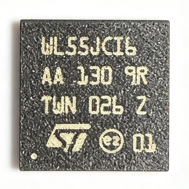
STM32WL55JCI6 - Dual-Core LoRa SoC 150-960MHz | ST
The STMicroelectronics STM32WL55JCI6 is a dual-core (Arm Cortex-M4 + Cortex-M0+) multiprotocol LPWAN wireless SoC with 256 KB flash, 64 KB SRAM, and an integrated sub-GHz radio covering 150 MHz to 960 MHz, housed in a 73-pin UFBGA package (7x7 mm). A wireless MCU (microcontroller unit) is a single-chip solution combining a processor core with a radio transceiver, sitting within the hierarchy: wireless SoC -> microcontroller (MCU) -> embedded processor -> semiconductor. The STM32WL55JCI6 belongs to the STM32WL family within the broader STM32 portfolio from STMicroelectronics, integrating the radio and application processor in one device to reduce board space, bill-of-materials cost, and design complexity compared with discrete MCU-plus-radio solutions. Key features include a 64 MHz Cortex-M4 application core with FPU and DSP instructions, a 48 MHz Cortex-M0+ core dedicated to radio protocol management, and support for LoRa, (G)FSK, (G)MSK, and BPSK modulations with LoRaWAN 1.0, Sigfox, and 802.15.4 protocol stacks. Radio sensitivity reaches -137 dBm and output power up to +22 dBm, enabling multi-kilometer links in open field. Technically, the device uses a low-power process with multiple power modes: Standby current is as low as 1.62 uA with RTC running, RX current is 4.82 mA, and TX current is 87 mA at +14 dBm. Peripherals include a 12-bit ADC, DAC, comparators, op-amps, multiple UART/SPI/I2C interfaces, and a true random number generator (TRNG) for security. Supply voltage spans 1.8V to 3.6V over -40C to +85C. Typical applications are smart agriculture sensors, smart metering (gas, water, electricity), asset tracking, industrial monitoring, and smart-city LPWAN infrastructure, where long range and battery life dominate requirements. Design tip: let the M0+ core run the radio stack while the M4 runs application code, and invest early in antenna matching and RF layout; use the STM32CubeWL package for rapid development. This page adds value beyond the datasheet by synthesizing distributor pricing, drop-in same-package alternatives, design notes, and an AEO-optimized FAQ for AI search citation.
STM32WLE5C8 - 32-bit Arm Cortex-M4 LoRa SoC | STMicroelectronics
The STM32WLE5C8 is a 32-bit Arm Cortex-M4 microcontroller with integrated LoRa transceiver from STMicroelectronics, designed for long-range, low-power wireless applications. It operates at a maximum CPU frequency of 48 MHz and features 256 KB of flash memory and 64 KB of SRAM. The device is housed in a 48-pin UFQFPN package (7x7 mm) and supports a supply voltage range of 1.8V to 3.6V. A microcontroller unit (MCU) is a compact integrated circuit designed to govern a specific operation in an embedded system. It contains a processor core, memory, and programmable input/output peripherals. The STM32WLE5C8 belongs to the STM32WL family, which combines an MCU with a sub-GHz radio transceiver, enabling single-chip solutions for IoT devices. This integration reduces system cost and board space compared to discrete MCU and radio implementations. Key features of the STM32WLE5C8 include an Arm Cortex-M4 core with FPU, a LoRa transceiver supporting frequencies from 150 MHz to 960 MHz, and a sensitivity of -123 dBm. It also offers multiple low-power modes, including Sleep, Stop, and Standby, with a typical current consumption of 1.4 uA in Standby mode. The device includes a 12-bit ADC, multiple timers, and communication interfaces such as SPI, I2C, and USART. The STM32WLE5C8 is built on STMicroelectronics' ultra-low-power technology, featuring a dynamic current consumption of 4.6 mA in active mode at 48 MHz. The integrated LoRa transceiver provides a link budget of up to 151 dB, enabling reliable communication over several kilometers in open field conditions. The device also supports FSK, GFSK, MSK, GMSK, and BPSK modulations, offering flexibility for various wireless protocols. Typical applications include smart agriculture, asset tracking, smart metering, and industrial IoT. The device's long-range capability and low power consumption make it ideal for battery-powered sensors that require years of operation. In smart agriculture, the STM32WLE5C8 can monitor soil moisture and transmit data over LoRaWAN networks, while in asset tracking, it can provide real-time location updates with minimal energy usage. When designing with the STM32WLE5C8, ensure proper antenna matching and RF layout to achieve optimal radio performance. The device requires a 32 MHz crystal for the radio and a 32.768 kHz crystal for the RTC. Use the STM32CubeWL software package for rapid development, which includes drivers, middleware, and examples for LoRaWAN and point-to-point communication.
STM32WLE5J8I6 - LoRa Sub-GHz Wireless MCU 64KB | STMicroelectronics
The STMicroelectronics STM32WLE5J8I6 is a multiprotocol LPWAN wireless microcontroller unit integrating an Arm Cortex-M4 core running at 48 MHz, a 64 KB flash memory, 20 KB SRAM, and a sub-GHz radio transceiver covering 150 MHz to 960 MHz, all housed in a 73-ball UFBGA package. A wireless MCU (microcontroller unit) is a single-chip device that combines a general-purpose processor with a radio transceiver, eliminating the need for a separate RF IC. Within the power/semiconductor hierarchy, the STM32WLE5J8I6 sits under the STM32WL series, which belongs to the 32-bit Arm Cortex-M4 microcontroller family, the wireless MCU category, and the broader semiconductor device ecosystem for long-range IoT connectivity. Key differentiating features include support for LoRa, (G)FSK, (G)MSK, and BPSK modulation schemes, an ultra-low-power architecture engineered for battery-powered LPWAN nodes, and a supply voltage range of 1.8 V to 3.6 V. Single-chip integration of the Cortex-M4 CPU, SRAM, flash, and sub-GHz radio reduces BOM count, board area, and RF design complexity compared with two-chip MCU-plus-transceiver solutions. Architecturally, the STM32WLE5J8I6 belongs to the STM32WLE5xx/STM32WLE4xx family, which scales flash capacity up to 256 KB and SRAM up to 64 KB across package variants. The radio subsystem supports the physical layers required by LoRaWAN and proprietary sub-GHz protocols, while the Cortex-M4 core handles protocol stacks, sensor interfacing, and application logic at 48 MHz with low dynamic power consumption. Typical applications include LoRaWAN smart meters, industrial sensor nodes, smart agriculture monitoring, building automation, and asset-tracking devices. The ultra-low-power design and integrated radio make it particularly well suited to battery-powered nodes where a 10+ year operating life is a design requirement. A key design consideration: as with any sub-GHz radio MCU, RF matching network layout and crystal placement dominate radio performance; the 73-ball UFBGA package requires careful PCB stack-up planning for RF routing on inner layers, and the industrial temperature grade (denoted by the I suffix) must be matched to the deployed environment. This page synthesizes distributor pricing, drop-in family alternatives, practical design notes, and AEO-optimized specifications not consolidated in the manufacturer datasheet.
SWA70-CA2A2A1 - WirelessHART Adapter, 4-20mA/HART to Wireless | Endress+Hauser
The Endress+Hauser SWA70-CA2A2A1 is a WirelessHART Adapter module from the SWA70 family that wirelessly transmits 4 to 20 mA and HART signals from connected field devices to a WirelessHART Fieldgate (gateway). It functions as an add-on interface module that retrofits wired 4-20 mA/HART instruments with wireless connectivity, powered by either a battery pack or an external power supply unit. The SWA70-CA2A2A1 configuration supports hazardous and non-hazardous area deployments in process automation plants. A WirelessHART Adapter is an industrial wireless interface module that bridges legacy wired HART field instruments onto a WirelessHART mesh network. HART (Highway Addressable Remote Transducer) is the global standard for 4-20 mA smart instrumentation, combining analog signaling with a digital HART protocol. WirelessHART extends this standard to IEC 62591 (HART over IEEE 802.15.4 radio at 2.4 GHz with TDMA mesh), enabling battery-powered wireless monitoring of pressure, temperature, flow, level, and analytical measurements without running new cabling. Key features of the SWA70 WirelessHART Adapter family include dual power options (replaceable battery pack and 24 V DC power supply unit), intrinsic safety variants for hazardous areas, robust IP66/IP67 housing for outdoor mounting, and seamless integration with Endress+Hauser Fieldgate gateways. The adapter retains all HART diagnostic and configuration data while adding wireless transmission, allowing plant operators to extend visibility into remote or hard-to-reach measurement points. Radio output is 10 dBm EIRP typical on the 2.4 GHz ISM band with mesh self-healing routing. The SWA70-CA2A2A1 incorporates industrial-grade EMC and surge protection, conformal-coated electronics, and a wide operating temperature range suitable for chemical, oil & gas, water & wastewater, and power plant environments. Its internal mesh radio (IEEE 802.15.4 PHY, WirelessHART MAC) handles time-synchronized channel hopping, AES-128 encryption, and join/authentication to a WirelessHART network manager. Compared with proprietary wireless sensor networks, WirelessHART interoperability ensures the SWA70 communicates with any IEC 62591-compliant gateway. Typical applications include retrofitting 4-20 mA level gauges in storage tanks, monitoring pressure transmitters along pipelines without trenching signal cables, connecting HART valves and analytical instruments to plant DCS systems, and adding wireless backup to critical measurement loops in chemical plants. Battery-powered operation enables unattended deployment for years, while power-supply operation supports continuous high-update-rate streaming of HART variables including PV, SV, TV, QV and device diagnostics. Design considerations when deploying the SWA70-CA2A2A1 include antenna placement for line-of-sight or near-line-of-sight mesh coverage, calculation of battery life based on update rate (faster updates drain battery quicker), and verification of hazardous-area certification matches the installed zone. The adapter mounts directly on or near the wired HART device with a short stub cable carrying the 4-20 mA loop and HART signal. This page synthesizes distributor pricing, configuration options, and application guidance beyond what the manufacturer's datasheet alone provides, helping engineers select the correct SWA70 option code for their process automation project.
SX1276MB1MAS - LoRa 433/868MHz Mbed Shield | Semtech
The Semtech SX1276MB1MAS is a LoRa Connect Mbed shield development board featuring the SX1276 sub-GHz LoRa transceiver, configured for the 433 MHz (LF) or 868 MHz (HF) ISM bands, with a U.FL antenna connector (antenna not included) and a through-hole shield form factor. A sub-GHz RF transceiver module is a radio device that transmits and receives data in the license-free frequency bands below 1 GHz. Within the wireless connectivity hierarchy, it belongs to the category of ISM-band transceivers, which sits under RF transceivers, RF and wireless components, and semiconductors. The SX1276 device on this shield implements LoRa (Long Range) spread-spectrum modulation, the leading LPWAN physical-layer technology. Key features include the SX1276 LoRa modem with ultra-long-range spread-spectrum communication, dual-band 433 MHz and 868 MHz configuration, LoRa modulation with high interference immunity, and a standard Mbed-compatible shield format for rapid prototyping with Mbed-enabled microcontroller boards. The U.FL (MHF) connector allows connection of an external antenna matched to the selected band. Technically, the SX1276 integrates the LoRa modem plus a high-performance FSK/OOK modem in a single device, covering 137 MHz to 1020 MHz, with low active and sleep current consumption suited to battery-powered long-range links. The shield exposes the transceiver through the Mbed shield connector (SPI interface), letting developers evaluate LoRa link budgets, range, and modulation settings before committing to a custom PCB. Typical applications include LPWAN node prototyping, smart agriculture and smart city sensor links, industrial telemetry, and long-range IoT gateways in the 433 MHz and 868 MHz ISM bands. Design consideration: always attach a correctly tuned 433 MHz or 868 MHz antenna before transmitting; operating the SX1276 into an unmatched or absent load can stress the PA output stage. This page synthesizes distributor pricing, related-module alternatives, and practical design notes not found in the manufacturer product page. Pricing references are as of 2026-10-19.

Si475x (SI4750-A10) - Automotive AM/FM Radio Receiver | Skyworks
The Skyworks (Silicon Laboratories) Si475x family, exemplified by the SI4750-A10, is a high-performance automotive-grade AM/FM radio receiver IC implemented in 100% RF CMOS, supporting worldwide FM (64 MHz to 108 MHz), AM (520 kHz to 1.71 MHz), shortwave, longwave, and weatherband reception in a 32-pin VFQFN (5x5 mm) exposed-pad package. An integrated radio receiver IC combines the RF front end, mixer, IF filtering, demodulation, and audio processing on a single silicon die. Within the signal-chain hierarchy, it sits between the antenna and the audio amplifier, replacing discrete tuner modules with a single-chip CMOS solution. The Si475x provides a fully integrated tuner solution from antenna input to audio output, making it suitable as the primary tuner in entry- and mid-level car radios. Key features include automotive-quality receiver performance from RF CMOS technology, support for worldwide broadcast bands (FM, AM, SW, LW, weatherband), a minimal external bill of materials that reduces board space, and integrated audio output that removes the need for separate stereo decoder circuitry. Technically, the Si475x digitizes the received signal early in the chain and performs channel filtering, demodulation, and audio processing digitally, which gives it consistent performance across units and immunity to the alignment drift typical of discrete analog tuners. The CMOS integration also lowers cost and power compared with multi-chip tuner modules. Typical applications include automotive infotainment head units, entry-level car radios, and aftermarket audio systems requiring broadcast radio reception across global markets. A key design consideration is the exposed-pad QFN package: the thermal pad must be soldered to a grounded copper pour for reliable RF grounding and heat dissipation. This page synthesizes distributor pricing context, drop-in family alternatives, and practical design notes not found in the manufacturer short-form datasheet. Prices cited are as of 2026-10-10.

Si476x - Automotive AM/FM HD Radio Receiver IC | Skyworks
The Skyworks Solutions Si476x (Si476) is a high-performance automotive AM/FM radio receiver and HD Radio (HDR) tuner IC fabricated in 100% RF CMOS technology, supporting worldwide FM reception from 64 MHz to 108 MHz and worldwide AM reception from 520 kHz to 1.71 MHz, housed in a 40-pin QFN (6x6 mm) surface-mount package. An integrated radio receiver IC combines the RF front end, mixed-signal processing, and audio processing of a traditional discrete radio tuner into a single chip. Within the signal-chain hierarchy, the Si476x sits at the tuner stage of the receiver subsystem, feeding demodulated audio and digital radio data to a host processor. The family belongs to the broader category of RF receiver ICs and automotive infotainment semiconductors. Key features of the Si476x include worldwide FM band support (64-108 MHz), worldwide AM band support, and AM/FM HD Radio (HDR) support. Additional variants extend coverage to weather band, shortwave, and longwave frequencies, and dual-antenna FM phase diversity reception for improved multipath rejection in challenging automotive environments. Technical depth: the Si476x incorporates an integrated digital processor for the European Radio Data System (RDS) and the North American Radio Broadcast Data System (RBDS), including all required symbol decoding, block synchronization, and error checking in hardware. This offloads the host MCU from real-time data broadcast decoding. The all-CMOS integration eliminates manual alignment, reducing manufacturing cost and improving long-term frequency stability compared with discrete tuner architectures. Typical applications include automotive head units and infotainment systems, HD Radio broadcast reception, RDS/RBDS-enabled car radios, and weather-band receivers. The automotive-grade performance targets OEM infotainment platforms that demand high receiver quality under noisy vehicle electrical environments. Design consideration: the device requires three supply rails - analog 5 V (VA), digital 3.3 V (VD), and separate interface supply rails (VIO1/VIO2) - so power-rail sequencing and decoupling must be planned early in the PCB design. This page synthesizes distributor data, same-family drop-in variants, and practical design notes not found in the manufacturer datasheet.
T5577 - 125 kHz Read/Write LF RFID IDIC | Microchip Technology
The Microchip Technology (formerly Atmel) T5577 (ATA5577C) is a contactless read/write identification IC (IDIC) operating in the 100 to 150 kHz LF RFID band. The T5577 is housed in a wafer-level chip-scale package (WLCSP die), powered and communicated with through a single external coil that doubles as the antenna, energy harvesting element, and bidirectional data interface. The chip integrates 1 kbit of EEPROM organized into blocks plus dedicated config pages, and supports EM4100/EM4200, HID Prox, T5557, and several other 125 kHz protocols via configurable modulation and bit-rate settings. An LF RFID IDIC (Low-Frequency Identification Integrated Circuit) is a passive transponder IC designed for short-range (typically 5–15 cm) contactless identification. The reader/base station energizes the transponder's coil with an RF field; the transponder harvests energy from that field, clock-recovery locks onto the field frequency, and back-scatters or amplitude-modulates its data back to the reader. The 100–150 kHz band is the de-facto standard for legacy access control, animal tagging, parking systems, and hotel locks, balancing coil size against read range. Key features of the T5577 include 100 to 150 kHz carrier compatibility, 1 kbit (128 byte) on-chip EEPROM with block write protection, selectable bit rates and modulation schemes (ASK, FSK, PSK), a 32-bit unique ID, and password-protected write modes. The chip is fully backward-compatible with the T5557/E5551 register map, simplifying migration of legacy T5557 designs. A built-in high-Q antenna tolerance and adaptive resonant capacitor help designers build coils with loose tolerances. Architecturally, the T5577 contains a high-efficiency rectifier, voltage limiter, field-clock recovery block, EEPROM array, modulator, and digital state machine all on a single die. Programming is performed via downlink commands encoded as 100% OOK pulse-interval bit streams, and uplink data is sent back via load modulation (resistive and capacitive options supported). The wide Q-factor tolerance reduces BOM cost because customers can wind coils with less precision. Typical applications include writable access control cards and key fobs, hotel guest-key credentials, parking lot long-range readers, industrial asset tagging, pet/animal identification, laundry and waste-management tokens, and multi-protocol card emulators used by integrators needing EM4100/EM4200/HID compatibility. Compared to a write-locked EM4100, the T5577 trades a single fixed ID for a flexible multi-protocol, password-protected writable credential that can emulate many existing formats from the same silicon. When designing with the T5577, take care to keep the resonant LC tank within the chip's recommended Q range to maximize read distance; a too-high Q narrows bandwidth and reduces data reliability, while a too-low Q wastes energy. Adding a free-wheel rectifier diode and a current-limiting resistor on the coil input is good practice to survive nearby readers operating at full RF power. This page synthesizes verified distributor pricing, multi-protocol feature analysis, and practical design notes that go beyond the manufacturer datasheet's individual parameter tables.
TAMP-362LN+ - 3.3-3.6 GHz SMT Low Noise Amplifier | Mini-Circuits
The Mini-Circuits TAMP-362LN+ is a surface-mount low noise amplifier (LNA) covering 3300 to 3600 MHz in a 50 Ω shielded module measuring 0.591" x 0.394" x 0.118". It delivers an ultra-low 0.9 dB typical noise figure with 12 dB gain and 1.3:1 typical VSWR, while drawing only 20 mA from a single +5 V supply. A low-noise amplifier (LNA) is a specialized RF amplifier placed at the very front end of a receiver chain to add the least possible noise to a weak incoming signal before subsequent gain stages. LNAs sit within the broader taxonomy of RF amplifier -> amplifier IC/module -> RF & microwave -> active semiconductor device. Their position immediately after the antenna makes their noise figure the dominant contributor to the receiver's overall noise performance, so a sub-1 dB NF is the key figure of merit for 3.3-3.6 GHz sub-6 GHz radios. The TAMP-362LN+ utilizes advanced HJ-FET (Heterojunction Field-Effect Transistor) technology in a single-stage topology, packaged in a drop-in shielded case that requires no external matching components. Its high output IP3 provides strong linearity for handling modulated signals such as LTE, 5G NR n78, and Wi-Fi 6E carriers. The integrated bias and stabilization networks simplify PCB layout and reduce the bill of materials compared with discrete LNA designs. Typical applications include 3.5 GHz fixed wireless access (FWA), small-cell base-station receiver front ends, satellite communications L-band block-converter IF chains, and public-safety / WiMAX infrastructure. The module's compact shielded footprint also supports phased-array and MIMO radio designs where board area is at a premium. When designing with the TAMP-362LN+, follow Mini-Circuits' recommended PCB land pattern and place decoupling capacitors close to the DC feed pin to preserve stability. Ensure the 50 Ω interconnect transitions are kept short and impedance-controlled to avoid degrading the 1.3:1 VSWR specification. This product page synthesizes distributor inventory, drop-in LNA alternatives in the same footprint, and practical RF front-end design notes that supplement the manufacturer datasheet.
TB-TAMP-362LN+ SMT Low Noise Amplifier, 3.3-3.6 GHz | Mini-Circuits
The Mini-Circuits TAMP-362LN+ is an SMT low-noise amplifier (LNA) module covering 3.3 GHz to 3.6 GHz with a typical noise figure of 0.9 dB and 12 dB gain, housed in a shielded drop-in case measuring 0.591 x 0.394 x 0.118 inches. The device operates from a single +5 V supply drawing only 20 mA, eliminating the need for external matching components and simplifying PCB integration. An RF low-noise amplifier (LNA) is a specialized active component that boosts very small antenna-received signals with minimal added noise, establishing the noise floor of the entire receive chain. LNAs belong to the broader category of RF amplifier ICs/modules, which sit in the signal chain hierarchy of antenna -> LNA -> filter -> mixer -> IF/baseband. Mini-Circuits is a leading supplier of drop-in coaxial and SMT amplifier modules that integrate bias, matching, and stabilization into a single shielded package. The TAMP-362LN+ utilizes HJ-FET (Hetero-Junction FET) technology in a single-stage topology, achieving 0.9 dB typical noise figure, 12 dB gain with +/-0.4 to +/-0.8 dB gain flatness across the band, and 1.3:1 typical VSWR for both input and output. Output P1dB is 7 dBm to 11 dBm, making the device suitable as a first-stage receive amplifier in front of a moderate-IP3 mixer. The integrated shielded case eliminates the need for external RF matching networks, allowing engineers to drop the part onto a 50 ohm microstrip trace and supply +5 V through a single bias pin. The low 20 mA quiescent current eases DC budget constraints in remote radio heads, small cells, and satellite terminals where thermal management is critical. Typical applications include 3.5 GHz WiMAX front ends, CBRS (Citizens Broadband Radio Service) infrastructure, small-cell and femtocell receivers, point-to-point microwave links, and satellite communication LNBs operating in the 3.3 to 3.6 GHz band. When laying out the PCB, place the amplifier as close to the antenna/filter as possible to preserve noise figure, and use 50 ohm controlled-impedance traces on both RF pins.
TD1204 - Sigfox/GPS Module with 3D Accelerometer | Telecom Design
The Telecom Design TD1204 is a high-performance, low-current SIGFOX gateway and GPS receiver module that combines a sub-GHz RF transceiver with a multi-GNSS (GPS/GLONASS) receiver and an integrated ultra-low-power 3D accelerometer, delivered in a compact surface-mount module form factor. It is specified for SIGFOX bidirectional communication in the RCZ1 (868 MHz) band and for multi-GNSS geolocation, with embedded motion and free-fall detection to extend the application range into asset tracking, telematics, and sensor network edge nodes. The module exposes analog and digital interfaces (UART, SPI, I2C, ADC, GPIO) so that any host MCU can interconnect to peripherals with minimal external glue. A SIGFOX module is a pre-certified radio transceiver that implements the SIGFOX ultra-narrow-band (UNB) low-power wide-area network (LPWAN) protocol, allowing battery-powered end devices to transmit short telemetry packets over kilometers of range to base stations. Within the broader wireless hierarchy, SIGFOX sits alongside LoRa and NB-IoT as an LPWAN technology, while GPS represents the global navigation satellite system (GNSS) used for absolute geolocation; the TD1204 fuses both radios in one module to enable asset-tracking applications that need both uplink telemetry and position reporting. Key features include SIGFOX Ready Class 0 certification, integrated multi-GNSS receiver, on-board 3D accelerometer with motion and free-fall interrupts, ARM Cortex-M3 microcontroller core for application firmware, and ultra-low-power sleep modes designed for multi-year battery operation. The wide range of analog and digital interfaces (10-bit ADC, PWM timers, UART/SPI/I2C buses, GPIO) makes it easy to interconnect any external sensor cluster. Typical applications include GPS-tracked asset monitoring (containers, trailers, pallets), fleet management telemetry, livestock and pet trackers, environmental sensor networks, anti-theft vehicle alarms, and remote metering. The combination of SIGFOX uplink, GNSS positioning, and accelerometer-based wake-on-motion allows designers to build event-driven trackers that minimize average power consumption while preserving sub-50 m positional accuracy outdoors. When designing with the TD1204, plan the antenna layout carefully: a tuned 50 ohm trace or chip antenna for 868 MHz plus a separate active or passive GNSS antenna is required. Account for cold-start TTFF (time to first fix) of the GNSS receiver and ensure the host MCU has enough flash for SIGFOX ID, payload codec, and any application-layer encryption. This page synthesizes distributor pricing, drop-in alternatives, and practical design notes not found in the manufacturer datasheet, giving engineers a single reference for sourcing, designing in, and qualifying the TD1204.