Produits (38 000+)

XC7A15T-1CSG324I - 16,640-LC Artix-7 FPGA | AMD
XC7A15T-1CSG324I

XC7A15T-1CSG324I - 16,640-LC Artix-7 FPGA | AMD

AMD XC7A15T-1CSG324I is an Artix-7 field-programmable gate array with 16,640 logic cells, 210 I/Os and 45 DSP slices in a 324-CSPBGA package. It uses 28 nm fabrication technology, operates from a 1 V core supply and is specified for the industrial temperature range of -40 °C to +100 °C junction temperature. The device is a cost-sensitive FPGA platform intended for compact, high-volume embedded systems requiring programmable logic, DSP and parallel I/O. An FPGA is a semiconductor whose digital logic, interconnect and signal-processing resources are configured after manufacture. Within the product hierarchy, an FPGA is a programmable-logic semiconductor and a reconfigurable digital IC. The XC7A15T belongs to AMD's Artix-7 family, combining general-purpose programmable logic with block RAM, DSP48 processing and high-performance I/O in a relatively small package. The verified specifications identify 16,640 logic cells, 210 I/Os, 921,600 internal configuration bits and 45 DSP slices. Its 324-CSPBGA package is identified in distributor records as a 324-LFBGA/CSPBGA, while an independent market listing specifies a 15 mm × 15 mm body. The -1 suffix denotes the device speed grade, the CSG324 suffix identifies the package, and the I suffix identifies industrial-temperature production. The Artix-7 architecture supports parallel processing, programmable I/O and dedicated DSP resources rather than implementing the complete design in fixed-function logic. This allows the same board design to be reused across multiple product variants through bitstream changes. The 45 DSP slices are especially relevant to filtering, fixed-point arithmetic, signal conditioning and control-loop workloads, while 210 I/Os support parallel buses, sensor acquisition and external memory interfaces. Typical applications include industrial automation, test and measurement, embedded control, communications, camera and image-processing interfaces, and compact instrumentation. The device is appropriate when deterministic parallel I/O and field-updatable logic are more valuable than the very high performance or very high logic density available from larger FPGA families. A complete design still requires suitable memory, clocking, power rails and high-speed PCB layout. Designers should use the AMD package pinout files and UG475 package guidance to map every CSG324 ball. Power, decoupling, configuration access, clocking and high-speed routing must follow the manufacturer's Artix-7 guidance. The industrial temperature rating applies to junction temperature and must be considered together with actual enclosure temperature, board heating and the device's power dissipation. This page consolidates verified distributor specifications, package details, temperature and speed-grade information into an engineering-focused selection reference. It also distinguishes documented drop-in options from unverified equivalents, provides comparison parameters, and identifies the application constraints that require datasheet and board-level review before procurement.

Devis Contact
XC7A15T-1FTG256C - 16,640-Cell Artix-7 FPGA | AMD
XC7A15T-1FTG256C

XC7A15T-1FTG256C - 16,640-Cell Artix-7 FPGA | AMD

The AMD XC7A15T-1FTG256C is an Artix-7 field-programmable gate array with 16,640 logic cells, 170 I/Os, and operation up to 464 MHz in a 256-ball FTBGA package. Designed for cost-sensitive, power-efficient embedded systems, this device combines programmable logic, DSP processing, block RAM, MMCM, PLL, and analog mixed-signal resources in a single 28 nm FPGA. An FPGA is a semiconductor whose digital logic, interconnect, and dedicated processing blocks are configured through a bitstream after fabrication. The Artix-7 family belongs to the broader programmable-logic hierarchy: FPGA, programmable logic device, digital semiconductor, and integrated circuit. This balance of logic density, I/O availability, and processing capability makes the XC7A15T suitable for embedded control, communications, industrial automation, machine vision, and prototype hardware. Key features include 16,640 programmable logic cells, 170 user I/Os, a maximum clock rating of 464 MHz, and a 950 mV to 1.05 V core-voltage range identified in the verified sources. The device also includes MMCM and PLL resources according to the product listing, along with DSP and analog mixed-signal capabilities described for the Artix-7 family. The -1 suffix identifies the device speed grade, while the C suffix denotes the commercial temperature option. The 256-ball FTBGA package supports dense board integration without relying on a large leaded footprint. Because a complete, verified ball-by-ball pin list was not included in the supplied source set, engineers should use AMD's official Artix-7 package pinout files before assigning signals, power planes, or configuration pins. Device configuration, I/O standards, and board-level connectivity must follow those package-specific files rather than general device assumptions. Typical uses include industrial controllers, communication equipment, machine-vision preprocessing, software-defined radio signal processing, sensor fusion, and rapidly deployed FPGA prototypes. In these systems, parallel programmable logic can implement interfaces or protocol engines, DSP slices can accelerate filters and transforms, and block RAM can buffer captured or transmitted data. Design planning should begin with AMD's Vivado or compatible FPGA design tools and the exact Artix-7 device constraints. Check timing at the selected -1 speed grade, validate I/O standards against the board, and plan decoupling and power delivery for the 0.95 V to 1.05 V core supply. This page combines verified catalog data, sourcing details, and engineering guidance beyond a basic distributor listing.

Devis Contact
XC7A15T-1FTG256I - 16,640-Cell Artix-7 FPGA | AMD
XC7A15T-1FTG256I

XC7A15T-1FTG256I - 16,640-Cell Artix-7 FPGA | AMD

The AMD XC7A15T-1FTG256I is an Artix-7 field-programmable gate array with 16,640 logic cells, 170 I/O, a 464 MHz operating frequency, and a 256-ball FTBGA package. Designed for the industrial temperature grade, it combines programmable logic, DSP processing, PLL and MMCM clocking, and analog mixed-signal resources in a cost-optimized FPGA platform. The device operates from a 950 mV to 1.05 V core supply range. An FPGA is a semiconductor whose digital and mixed-signal functions are defined by a downloadable configuration. Within the product hierarchy, an FPGA is a programmable logic device and a semiconductor, while Artix-7 is AMD's low-cost, low-power FPGA family. This positioning makes the XC7A15T useful where designers need flexible parallel processing, interface adaptation, control logic, or DSP without developing fixed-function silicon. The 16,640-cell Artix-7 fabric provides the core implementation capacity, while 170 I/Os support connections to external memories, converters, sensors, displays, and communications equipment. The listed 464 MHz figure establishes the device's advertised operating-frequency class. Integrated DSP, PLL, and MMCM resources reduce the need for separate clock-generation or arithmetic components when the required functions fit within the FPGA fabric. The -1 portion identifies the speed grade, FTG256 identifies the 256-ball package, and the final I indicates the industrial temperature grade. Verified distributor information identifies an industrial-temperature variant with the same logic density and package. Its 950 mV to 1.05 V supply range is important during power-supply design because the core, auxiliary rails, I/O standards, and configuration system must be planned together rather than treated as a single fixed-voltage domain. Typical uses include industrial automation and control, communications interface consolidation, sensor and instrumentation systems, video-processing pipelines, and low-cost embedded DSP. These application descriptions are consistent with the Artix-7 family's stated combination of programmable logic, DSP processing, clock management, and analog mixed-signal integration. For a new board, the FTG256 footprint requires a dense ball-layout PCB, careful power-plane design, and careful separation of sensitive analog or clock paths. For an existing design, migration requires checking the exact package pinout, supported I/O standards, configuration interface, power rails, timing constraints, and installed Vivado or another supported AMD implementation tool. This page consolidates verified distributor specifications, package and pinout resources, same-family drop-in candidates, practical design guidance, and a parameter comparison to support component selection and procurement. It does not substitute for the complete Artix-7 data sheet, package files, and design-tool timing reports.

Devis Contact
XC7A15T-2FTG256C - 16,640 LEs Artix-7 FPGA | AMD
XC7A15T-2FTG256C

XC7A15T-2FTG256C - 16,640 LEs Artix-7 FPGA | AMD

AMD XC7A15T-2FTG256C is an Artix-7 field-programmable gate array with 16,640 logic cells, 170 I/O, 921,600 RAM bits, and a 256-LBGA package. The -2 speed grade is intended for cost-sensitive, power-efficient designs requiring a balanced combination of programmable logic, DSP processing capability, and high-speed serial connectivity. It operates across the commercial temperature range of 0°C to +85°C and is available from distributors as a 256-LBGA FPGA. An FPGA is a reconfigurable digital semiconductor in which the logic, interconnections, and processing resources are configured after manufacture. Within the product hierarchy, the XC7A15T belongs to the Artix-7 FPGA family and combines a programmable logic array, block RAM, DSP resources, and general-purpose input/output blocks in one device. This integration allows designers to implement parallel data processing, control logic, protocol bridging, and interface functions on a single programmable chip. The principal verified device figures are 16,640 logic cells, 921,600 RAM bits, 170 I/O, and a 256-LBGA package. The -2 designation identifies its performance grade within the Artix-7 family. Its low-cost and power-efficient positioning makes it relevant to industrial automation, machine vision, telecommunications infrastructure, protocol conversion, baseband processing, wireless backhaul, and embedded control systems. The 256-LBGA package also supports compact, high-density board layouts. Technically, the device combines programmable logic fabric with dedicated memory and DSP blocks, allowing multiple data paths to be processed concurrently. The large 170-I/O count provides substantial connectivity for external memory, sensors, network transceivers, display interfaces, and control peripherals. Its 921,600 RAM bits support buffering and data storage within the FPGA fabric, while the dedicated DSP capability enables fixed-point filtering, transform, and signal-processing functions without requiring separate accelerators. Typical implementations place the FPGA beside high-speed transceivers, external memory, clock sources, and application-specific peripherals. Machine-vision designs can parallelize image acquisition and filtering, telecom equipment can perform line-card adaptation or protocol bridging, and industrial controllers can combine sensor acquisition with deterministic logic. Because FPGA resources are configurable, the same family can support multiple product variants without changing the PCB footprint when device density and speed-grade requirements permit. Designers should review the manufacturer Artix-7 datasheet and package pinout files before assigning bank voltages, clock pins, high-speed serial pins, and power rails. Decoupling, PCB return paths, thermal management, configuration interface access, and proper I/O standard selection are critical to reliable implementation. Although the 256-LBGA offers high I/O density, its fine-pitch routing and power-delivery requirements demand careful constraint-driven layout and multilayer PCB planning. This product data combines verified distributor pricing, Artix-7 family specifications, package information, and practical engineering guidance. It also distinguishes true same-package drop-in options from broader functional FPGA alternatives, helping engineers shortlist a device while still validating timing, power, configuration, and lifecycle requirements against the official AMD documentation.

Devis Contact
XC7A15T-3FTG256E - 16,640 Logic Cells, 170 I/O | AMD
XC7A15T-3FTG256E

XC7A15T-3FTG256E - 16,640 Logic Cells, 170 I/O | AMD

AMD XC7A15T-3FTG256E is an Artix-7 field-programmable gate array with 16,640 logic cells, 921,600 RAM bits, 170 I/O, and a 1 V operating voltage, housed in a 256-pin FTG256 ball grid array package. The -3 speed grade targets higher-performance designs, while the E suffix identifies the extended-temperature option. Built on 28 nm FPGA technology, this device combines programmable logic resources with embedded block RAM, programmable I/O, and configurable interface functionality. A field-programmable gate array, or FPGA, is a semiconductor whose logic, interconnect, memory, and I/O resources can be configured after manufacture. Within the product hierarchy, the XC7A15T belongs to the Artix-7 FPGA family and the broader programmable-logic semiconductor category. Its 16,640 logic cells provide moderate implementation capacity for embedded control, signal processing, communications, instrumentation, and general-purpose programmable systems. The verified device data identifies 921,600 RAM bits for embedded memory and 170 user I/O. Cross-reference material describes the device using either 2,600 logic blocks or 1,300 LAB/CLB groupings, reflecting different counting conventions for the same 16,640-logic-cell device. The target operates from a 1 V core supply, enabling the energy-efficient 28 nm architecture associated with the Artix-7 family. The FTG256 package uses 256 BGA sites and is intended for surface-mount PCB assembly. BGA construction supports compact designs but requires careful escape-routing, ground-plane continuity, via-in-pad considerations where appropriate, and assembly process control. AMD package pinout resources are available for board-layout validation, while the complete electrical and timing limits must be taken from the manufacturer data sheet. Typical uses include industrial automation, test and measurement, embedded video and control, low-cost communications equipment, sensor processing, and education or prototyping platforms. The 170 I/O make it especially relevant to designs needing multiple parallel digital interfaces while retaining substantial programmable logic capacity. Designers should verify power sequencing, decoupling, signal integrity, configuration interface requirements, and exposed thermal behavior against the manufacturer documentation. Migration candidates must be checked for package, speed grade, temperature range, configuration scheme, bank voltage, and pinout rather than relying on the XC7A15T family name alone. This product page consolidates verified distributor specifications, package and pinout resources, source links, and same-package migration options. It also distinguishes directly comparable speed and temperature variants from different-package devices that cannot be treated as drop-in replacements.

Devis Contact
XC7A200T-1FB484C - 215,360-LCell Artix-7 FPGA | AMD
XC7A200T-1FB484C

XC7A200T-1FB484C - 215,360-LCell Artix-7 FPGA | AMD

The AMD XC7A200T-1FB484C is an Artix-7 field-programmable gate array with 215,360 logic cells, 285 user I/Os, and a speed grade of 1 in a 484-ball FCBGA package. The device combines programmable logic, DSP resources, block RAM, programmable I/O, and dedicated clocking resources in a single low-power device for compact control, signal-processing, and communications systems. A field-programmable gate array is a semiconductor whose digital functionality is configured after manufacture. An FPGA belongs to the broader programmable-logic hierarchy, where it sits above basic programmable devices and provides substantially greater parallelism than a microcontroller or fixed-function logic device. The Artix-7 family combines that programmable flexibility with a programmable logic architecture optimized for low power consumption and high performance in cost-sensitive embedded systems. The XC7A200T-1FB484C provides 215,360 logic cells and 285 I/O positions, according to the AMD Artix-7 family data. Its speed grade 1 designation identifies the intended performance class, while the FCBGA package supports dense board-level connections for designs requiring substantial signal routing. The device also includes digital signal processing and memory resources, making it suitable for parallel data acquisition, signal conditioning, embedded control, and communication-interface functions. Artix-7 devices use configurable logic blocks, dedicated DSP slices, block RAM, and multiplexed input/output resources. These resources allow parallel datapaths to be implemented without relying on a sequence of processor instructions. The XC7A200T-1FB484C is particularly useful when several independent channels must be sampled, filtered, transformed, or checked concurrently, because fixed sequential processing can become a bottleneck as channel count increases. Typical uses include industrial automation, test and measurement equipment, medical instrumentation, embedded vision, audio and signal processing, communications infrastructure, and low-power embedded control. A board designer would normally pair the FPGA with external memory, clock sources, transceivers, analog converters, power regulators, and high-speed differential interfaces when the design exceeds the capabilities of the on-chip resources. The most important layout consideration is power and signal integrity. Place the decoupling network at each supply pin, provide a clean ground-plane structure, and follow the AMD package pinout and PCB design guidance for ball assignments and high-speed routing. Verify the exact power rails, configuration interface, and termination requirements against the manufacturer documentation before releasing the PCB. This page combines the component specifications, replacement options, application guidance, comparison data, and practical integration notes needed to evaluate the XC7A200T-1FB484C for a new programmable-logic design.

Devis Contact
XC7A200T-1FB484I - 215K-Cell Artix-7 FPGA | AMD | Industrial
XC7A200T-1FB484I

XC7A200T-1FB484I - 215K-Cell Artix-7 FPGA | AMD | Industrial

AMD XC7A200T-1FB484I is an Artix-7 field-programmable gate array built on 28 nm process technology, with 215,360 programmable logic cells, 285,000 system logic cells, and 485,360 register bits. The device is supplied in a 484-ball, lidless FCBGA package measuring 23 x 23 mm with a 1.0 mm ball pitch. Its ordering code identifies a speed grade of 1 and an industrial-temperature option. An FPGA is a programmable semiconductor in the broader hierarchy of programmable logic devices, logic integrated circuits, and digital semiconductors. Artix-7 devices combine configurable logic, block RAM, programmable input/output, and dedicated clocking resources on one device. This combination allows designers to implement parallel digital logic, interface adaptation, signal processing, and embedded control functions without relying on a fixed application-specific circuit. The XC7A200T-1FB484I provides 215,360 logic cells, 134,553,60 as presented by the distributor record, 485,360 register bits, and an operating core voltage identified as 1 V. The industrial ordering suffix selects extended-temperature suitability, while the speed-grade 1 suffix indicates the device performance class within the Artix-7 family. Its 484-ball fine-pitch package supports high-density connections while requiring careful PCB layout, thermal analysis, and assembly control. The Artix-7 architecture is suitable for designs that require more parallelism than a microcontroller or discrete logic implementation can provide. Its fabric can host parallel data paths, control state machines, protocol bridges, and fixed-pipeline processing blocks. Dedicated memory resources support buffering and data alignment, while programmable I/O can accommodate multiple interface standards within the electrical limits of the selected banks and package pins. Typical applications include industrial automation, camera and imaging control, communications infrastructure, test and measurement systems, instrumentation, and embedded signal-processing equipment. The device is also appropriate for prototype platforms where programmable logic allows interfaces, timing, and control algorithms to be revised without changing the PCB. The primary design consideration is the fine-pitch BGA land pattern. A qualified PCB stack-up, escape-routing strategy, power-distribution network, and assembly process are necessary for reliable manufacture. Designers should also confirm the exact pinout, supported I/O standards, configuration method, and power requirements in AMD package documentation before releasing the hardware. This product record combines the verified device identity, package information, family-level architecture, and engineering guidance with commercial forms for quotation, availability, and lifecycle review. It also provides focused selection criteria for distinguishing speed-grade, temperature-grade, and package variants before design commitment.

Devis Contact
XC7A200T-1FB676I - 215K-Cell Artix-7 FPGA | AMD
XC7A200T-1FB676I

XC7A200T-1FB676I - 215K-Cell Artix-7 FPGA | AMD

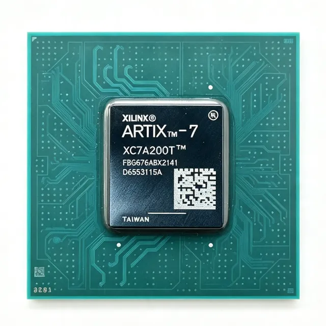
The AMD XC7A200T-1FB676I is an Artix-7 field-programmable gate array with 215,360 logic cells, 400 I/O, 28 nm process technology, and a 676-pin FCBGA package. It combines programmable logic density with integrated memory, clock-management, and high-speed transceiver capabilities for cost-sensitive embedded, industrial, communications, and signal-processing systems. An FPGA is a semiconductor whose digital circuits are configured after manufacture. Within the product hierarchy, the XC7A200T is an Artix-7 FPGA, a configurable logic device within the broader programmable-logic and semiconductor categories. Unlike a fixed-function microcontroller or application-specific integrated circuit, an FPGA allows designers to implement parallel processing, custom interfaces, control logic, and hardware acceleration in one device. The device provides 215,360 logic cells, 400 I/O, 13,455,360 bits of block RAM, and a nominal 1 V operating class, according to the AMD Artix-7 datasheet. The 28 nm fabrication process supports a compact implementation with configurable logic resources for data acquisition, protocol handling, image processing, embedded control, and communications infrastructure. The -1 suffix identifies the device speed grade, while the -I suffix identifies the associated temperature or qualification option. The FBG676 package provides 676 ball-grid contacts and supports the high I/O count needed by systems combining parallel data paths, external memory, high-speed serial links, and general-purpose control. Package-specific decoupling, power delivery, and escape-routing guidance must follow the AMD package data. Typical applications include industrial automation, test and measurement, communications infrastructure, video and image processing, embedded control, and high-throughput signal acquisition. In these systems, programmable parallel pipelines can process multiple samples or lanes concurrently, while integrated block RAM reduces external-memory pressure for buffers, packet descriptors, and look-up data. When planning the PCB, provide independent 28 nm FPGA power rails with low-impedance distribution and place bulk and high-frequency decoupling close to the package. Match ball escape routing to the selected board stack-up and verify high-speed transceiver, memory-interface, and differential-I/O constraints against the AMD pinout and layout guidance. This product page combines the key electrical and packaging facts, practical replacement analysis, comparison parameters, and design guidance needed to evaluate the XC7A200T-1FB676I for a new programmable-logic design.

Devis Contact
XC7A200T-1FBG484I - 740K Logic Cells FPGA | AMD Xilinx
XC7A200T-1FBG484I

XC7A200T-1FBG484I - 740K Logic Cells FPGA | AMD Xilinx

The AMD Xilinx XC7A200T-1FBG484I is a high-performance Artix-7 family FPGA delivering 740K logic cells, 215K logic slices, and 13 Mb of block RAM in a 484-ball FBGA package. It operates from 0.95V to 1.05V core voltage and supports up to 285 user I/O pins with multiple I/O standards including LVCMOS, LVDS, and HSTL. The device features 740 DSP48E1 slices for high-speed digital signal processing and 10 clock management tiles (CMTs) for robust clock generation and distribution. An FPGA (Field-Programmable Gate Array) is a semiconductor device containing programmable logic blocks and interconnects that can be configured after manufacturing to implement custom digital circuits. FPGAs sit between ASICs (application-specific integrated circuits) and microprocessors in the design hierarchy, offering the flexibility of software-defined hardware with the parallelism of dedicated logic. The Artix-7 family is optimized for cost-sensitive, high-volume applications requiring high logic density and low power, positioned below the Kintex-7 and Virtex-7 families in AMD's 7-series portfolio. Key features include 285 user I/O pins supporting up to 1.25 Gbps LVDS, 740 DSP48E1 slices with 25x18 multiplier capability, and 10 CMTs providing PLL and MMCM functions. The device also offers 13 Mb of block RAM organized as 365 36Kb blocks, enabling substantial on-chip data storage. The -1 speed grade provides balanced performance with 550 MHz maximum clock frequency, while the industrial temperature range (-40C to +100C) ensures reliable operation in harsh environments. The XC7A200T-1FBG484I is built on AMD's 28nm high-k metal gate (HKMG) process technology, delivering high performance with low static power. The architecture includes configurable logic blocks (CLBs) with 6-input look-up tables (LUTs), dedicated carry chains for arithmetic functions, and shift register capabilities. The device supports partial reconfiguration, allowing dynamic updates to logic functions without full device reprogramming, which is valuable for adaptive systems. Typical applications include software-defined radio (SDR), medical imaging, industrial motor control, and high-performance computing acceleration. The high DSP count and low-latency I/O make it ideal for real-time signal processing in communications and defense systems. The 484-ball FBGA package with 1.0mm ball pitch enables compact PCB designs while providing adequate thermal dissipation for moderate power levels. When designing with this FPGA, ensure adequate decoupling capacitors on all power rails (VCCINT, VCCAUX, VCCO) and follow AMD's PCB design guidelines for high-speed I/O. The configuration interface supports multiple modes including JTAG, SPI, and SelectMAP, allowing flexible system integration. Power sequencing must follow the recommended ramp rates to avoid latch-up or configuration failures.

USD $38,50 Contact
XC7A200T-1FBG676I - 740K Logic Cells FPGA | AMD Xilinx | FBG676
XC7A200T-1FBG676I

XC7A200T-1FBG676I - 740K Logic Cells FPGA | AMD Xilinx | FBG676

The AMD Xilinx XC7A200T-1FBG676I is a high-performance Artix-7 family FPGA delivering 740K logic cells, 215,360 logic slices, and 13,140 Kb of Block RAM in a 676-ball FCBGA (FBG676) package. It operates with a core voltage of 1.0V and supports I/O standards up to 3.3V, making it suitable for a wide range of high-speed digital designs. Data verified as of 2026-08-05. An FPGA (Field-Programmable Gate Array) is an integrated circuit that can be configured by the designer after manufacturing, offering reconfigurable logic blocks and programmable interconnects. FPGAs sit within the broader hierarchy of programmable logic devices (PLDs), which are a subset of digital integrated circuits. They provide a flexible alternative to ASICs, enabling rapid prototyping and hardware acceleration without the high NRE costs of custom silicon. Key features include 740K logic cells, 365 DSP48E1 slices, 10.5 Mb of distributed RAM, and 13,140 Kb of Block RAM. The device supports up to 400 I/O pins with SelectIO technology, offering programmable I/O standards and speeds. It also includes integrated PCIe blocks, Gigabit Transceivers (GTX) for high-speed serial communication, and a XADC for analog-to-digital conversion, providing a comprehensive platform for complex digital systems. The Artix-7 architecture is built on a 28nm high-k metal gate (HKMG) process, balancing performance and power efficiency. The device features a configurable logic block (CLB) structure with 6-input LUTs, dedicated carry chains, and flip-flops, enabling efficient implementation of complex logic functions. The DSP48E1 slices support high-speed arithmetic operations, while the Block RAM provides on-chip storage for data buffering and FIFO implementations. Typical applications include software-defined radio (SDR), medical imaging, industrial motor control, and high-performance computing acceleration. The high logic density and DSP resources make it ideal for signal processing tasks, while the transceivers enable high-speed data communication in networking and broadcast equipment. When designing with this FPGA, careful attention must be paid to power supply decoupling and thermal management. The device requires multiple supply rails (VCCINT, VCCAUX, VCCO) with proper sequencing, and the 676-ball BGA package demands a multi-layer PCB with adequate thermal vias for heat dissipation. This page synthesizes distributor pricing, drop-in alternatives, and practical design notes not found in the AMD datasheet.

USD $390,00 Contact
XC7A200T-1SB484I - 215K Logic Cell Artix-7 FPGA | AMD
XC7A200T-1SB484I

XC7A200T-1SB484I - 215K Logic Cell Artix-7 FPGA | AMD

The AMD XC7A200T-1SB484I is an Artix-7 field-programmable gate array with 215,360 logic cells, 13,455,360 RAM bits, 16,825 configurable logic blocks, and 285 I/Os in a 484-ball FCBGA package. It is manufactured on a 28 nm process and operates from a 1 V core supply. The -1 speed grade, SB484 package designation, and industrial-temperature suffix organize the device for design, sourcing, and qualification workflows. An FPGA is a programmable semiconductor in the broader semiconductor and digital-logic hierarchy. Unlike a fixed-function application-specific integrated circuit, an FPGA combines programmable logic, block RAM, digital signal processing resources, and programmable I/O in one device. Artix-7 devices balance logic density, embedded memory, signal-processing capability, and low-cost packaging for designs requiring reconfigurable hardware or substantial parallel processing. The XC7A200T provides 215,360 logic cells and 13,455,360 RAM bits, giving designers substantial capacity for control logic, protocol bridges, data acquisition, embedded vision, and digital signal processing. The device also includes 740 DSP slices according to the Artix-7 family specification summary. Its 285 I/Os provide substantial connectivity for parallel sensors, converters, memories, and communications interfaces. The XC7A200T belongs to the Artix-7 product family, whose programmable architecture combines logic cells, block RAM, DSP slices, dedicated clocking resources, and programmable input/output. The 28 nm fabrication process supports a compact and power-efficient implementation for industrial, communications, instrumentation, and embedded-control systems. Configuration storage and the programming interface allow the same board design to support multiple hardware functions when field updates are required. Typical uses include industrial data-acquisition systems, sensor and signal-processing platforms, communications infrastructure, embedded control, high-speed interface bridges, and machine-vision preprocessing. A 484-ball FCBGA also supports dense, high-speed PCB layouts with short escape paths, but it requires careful via-in-pad, solder-mask, and thermal-management practices. The package outline is 19 mm by 19 mm according to the product listing. When planning a board, verify the SB484 ball map, differential-pair assignments, supply sequencing, and exposed thermal requirements against the AMD Artix-7 package documentation. The high pin count increases routing density, so ball-grid-array escape routing and power-plane integrity can be more consequential than they would be in a smaller package. Use the manufacturer’s pinout files and board-design guidance rather than inferring ball assignments from another Artix-7 package. This page combines device specifications, package-aware alternatives, direct comparison parameters, and practical implementation guidance. It is designed to help engineers identify the correct Artix-7 density, speed grade, and package before committing to a high-pin-count PCB layout.

Devis Contact
XC7A200T-2FB484I - 215K Logic Cell Artix-7 FPGA | AMD
XC7A200T-2FB484I

XC7A200T-2FB484I - 215K Logic Cell Artix-7 FPGA | AMD

The AMD XC7A200T-2FB484I is an Artix-7 field-programmable gate array with 215,360 logic cells, 13,455,360 RAM bits, and 285 I/O positions, housed in a 484-ball FCBGA package. Built on a 28 nm process, the device combines programmable logic, block RAM, digital signal processing resources, and four GTP transceiver channels in a low-cost FPGA platform intended for compact, high-performance embedded systems. An FPGA is a semiconductor whose digital logic, interconnections, and input/output behavior are configured after manufacture. The Artix-7 family belongs to the broader FPGA hierarchy, which sits above fixed-function logic and programmable signal-processing devices. Compared with an ASIC, an FPGA permits design revisions, hardware reuse, and rapid prototyping without fabricating a custom integrated circuit. Its configurable parallel processing fabric is especially useful for image pipelines, control systems, communications, and data acquisition. The XC7A200T-2FB484I provides 13,455,360 RAM bits for buffers, packet storage, and general-purpose logic. Its 285 I/O positions support integration with external memory, control signals, serial transceivers, and industrial peripherals. Four GTP channels support high-speed serial links, while the -2 speed grade identifies a performance grade within the Artix-7 portfolio. The industrial-temperature suffix supports designs intended for extended-temperature operation. Artix-7 devices use a programmable fabric organized into configurable logic blocks and programmable interconnect resources. This architecture allows parallel datapaths to operate simultaneously, making the device suitable for video acquisition, sensor fusion, protocol bridging, and embedded control. Because FPGA designs depend on clocks, I/O standards, power rails, and tool-supported constraints, the device must be paired with an appropriate clocking scheme, power architecture, and device-aware PCB design. Typical applications include industrial machine vision, test and measurement equipment, embedded communications, radar or signal-processing front ends, and compact control systems. The 484-ball package supports dense connections but requires careful escape routing and multilayer PCB construction. Four GTP links are valuable for high-speed serial interfaces, while the large logic and RAM resources support parallel processing and substantial data buffering. A key design consideration is that the 484-ball FCBGA package requires a constrained, multilayer PCB with controlled power and ground distribution. Use the AMD package pinout files and the device-specific pin constraints when assigning banks, differential pairs, power pins, and transceiver connections. Confirm the selected clocking, memory interface, and I/O standards before finalizing the schematic and layout. This product record combines device resource details, package information, verified source links, comparison guidance, and practical PCB-design considerations to accelerate component selection and board planning.

Devis Contact
XC7A200T-2FB676I - 215K Artix-7 FPGA | Advanced Micro Devices
XC7A200T-2FB676I

XC7A200T-2FB676I - 215K Artix-7 FPGA | Advanced Micro Devices

Advanced Micro Devices XC7A200T-2FB676I is an Artix-7 field-programmable gate array with 215,360 logic cells, 400 I/O, 33,650 adaptive logic modules, and a 676-ball FCBGA package. The device uses 28 nm FPGA technology, operates from a 1 V core supply, and is built around the 215K XC7A200T logic resource configuration for programmable control, signal processing, and interface designs. An FPGA is a programmable semiconductor containing configurable logic blocks, programmable I/O, block RAM, DSP resources, and dedicated clocking circuitry. Within the device hierarchy, the XC7A200T belongs to the Artix-7 FPGA family, the Xilinx/AMD FPGA portfolio, and the broader category of programmable logic devices. Its large fabric allows parallel architectures that are difficult to implement with fixed-function processors or conventional discrete logic. The Artix-7 architecture provides 215,360 logic cells, 33,650 adaptive logic modules, 13.32 Mbit of block RAM, 740 DSP slices, and 400 user I/O according to the AMD Artix-7 family information. The -2 speed grade supports higher performance than the -1 grade, while the industrial I suffix identifies the intended temperature range. MMCM, PLL, and DSP resources support clock generation, timing, and arithmetic-heavy signal-processing pipelines. The XC7A200T-2FB676I combines programmable logic with integrated memory and DSP capacity. A design can use parallel lanes for image processing, protocol bridging, fixed-point arithmetic, or general-purpose data acquisition. Its 400 I/O provide substantial connectivity, while the FCBGA-676 package supports fine-pitch escape routing and requires careful power, ground, and differential-pair layout in multilayer PCBs. Typical uses include industrial control, test and measurement, communications infrastructure, embedded video processing, robotics, and high-throughput data conversion. The large fabric is particularly useful when an application requires deterministic parallel operation, flexible I/O, or hardware acceleration without replacing an FPGA with a larger processor-based system. The main design consideration is package complexity. The 676-ball FCBGA requires a dense escape-routing strategy, multiple power rails, carefully controlled decoupling, and assembly-process alignment. Use the AMD package pinout files and UG475 when assigning balls and planning the PCB stackup, and complete signal-integrity and power-integrity simulations before fabrication. This page combines the Artix-7 device specification with package-aware alternatives, application guidance, and design notes intended to accelerate schematic capture, PCB planning, and sourcing decisions for XC7A200T-2FB676I implementations.

Devis Contact
XC7A200T-2FBG484C - Artix-7 FPGA 740K Logic Cells | AMD Xilinx
XC7A200T-2FBG484C

XC7A200T-2FBG484C - Artix-7 FPGA 740K Logic Cells | AMD Xilinx

The AMD Xilinx XC7A200T-2FBG484C is a high-performance Artix-7 family FPGA delivering 740K logic cells, 215K logic slices, and 13 Mb of block RAM in a 484-ball FBGA package. It operates with a core voltage of 1.0V and supports I/O standards from 1.2V to 3.3V, making it suitable for a wide range of applications. Data verified as of 2026-08-04. An FPGA (Field-Programmable Gate Array) is an integrated circuit that can be configured by the customer or designer after manufacturing. It consists of programmable logic blocks, configurable interconnects, and I/O blocks, allowing for flexible implementation of digital circuits. FPGAs sit within the broader category of programmable logic devices (PLDs), which are part of the semiconductor industry. They are used in applications requiring parallel processing, high-speed I/O, and reconfigurable logic, such as communications, industrial automation, and aerospace. Key features of the XC7A200T-2FBG484C include 740K logic cells, 215K logic slices, 13 Mb of block RAM, 740 DSP slices, and 10.3 Mb of distributed RAM. It also features 16 GTX transceivers supporting up to 6.6 Gbps, 10 clock management tiles (CMTs), and 285 user I/O pins. The device supports multiple I/O standards including LVCMOS, LVDS, and HSTL, and includes hardened memory controllers for DDR3 and DDR4. The Artix-7 architecture is built on a 28nm high-k metal gate (HKMG) process, offering a balance of performance, power, and cost. The device includes advanced clocking resources, such as PLLs and MMCMs, and supports partial reconfiguration for dynamic logic updates. The 484-ball FBGA package provides a compact footprint with excellent thermal and electrical characteristics, enabling high-density designs. Typical applications include software-defined radio (SDR), medical imaging, motor control, and high-performance computing. The high logic density and DSP slices make it ideal for signal processing, while the GTX transceivers support high-speed serial communication in networking and video applications. When designing with this FPGA, careful attention must be paid to power supply decoupling and thermal management. The device requires multiple supply rails (VCCINT, VCCAUX, VCCO) and a proper power-up sequence. Use the Xilinx Power Estimator (XPE) to calculate power consumption and design an appropriate thermal solution. This page synthesizes distributor pricing, drop-in alternatives, and practical design notes not found in the AMD Xilinx datasheet, providing a comprehensive resource for engineers.

USD $320,00 Contact
XC7A200T-2FBG484I - Artix-7 FPGA 215K Logic Cells | AMD Xilinx
XC7A200T-2FBG484I

XC7A200T-2FBG484I - Artix-7 FPGA 215K Logic Cells | AMD Xilinx

The AMD Xilinx XC7A200T-2FBG484I is a high-performance Artix-7 family FPGA featuring 215,360 logic cells, 16,825 CLBs, and 13,455,360 bits of Block RAM, packaged in a 484-ball FBGA (FBG484) with a -2 speed grade and industrial temperature range (-40°C to +100°C). It delivers 285 user I/O pins, making it ideal for high-bandwidth signal processing and connectivity applications. An FPGA (Field-Programmable Gate Array) is a semiconductor device containing programmable logic blocks and interconnects that can be configured after manufacturing to implement custom digital circuits. FPGAs sit within the broader category of programmable logic devices (PLDs), which are part of the application-specific integrated circuit (ASIC) family, but offer reconfigurability that ASICs lack. The Artix-7 family is positioned as a mid-range FPGA optimized for cost-sensitive, high-volume applications requiring high-speed transceivers and DSP capabilities. Key features include 740 DSP48E1 slices for high-throughput digital signal processing, 16 high-speed transceivers supporting up to 6.6 Gb/s, and 285 I/O pins with support for multiple I/O standards including LVCMOS, LVDS, and HSTL. The device also integrates a PCIe Gen2 block, 10/100/1000 Ethernet MACs, and an analog-to-digital converter (XADC) for system monitoring. The -2 speed grade provides balanced performance for logic and I/O, while the industrial temperature range ensures reliable operation in harsh environments. Architecturally, the XC7A200T is built on the 28nm high-k metal gate (HKMG) process, offering a 50% lower power footprint compared to previous generations. The configurable logic blocks (CLBs) contain 6-input look-up tables (LUTs) and dual flip-flops, enabling efficient implementation of complex logic functions. The device supports partial reconfiguration, allowing dynamic updates to specific regions without disrupting the entire design. Typical applications include software-defined radio (SDR), medical imaging, industrial motor control, and high-performance computing acceleration. The high transceiver count and DSP resources make it particularly suited for communications infrastructure, such as LTE/5G base stations and network switches, where high-speed serial links and parallel processing are essential. When designing with this FPGA, careful attention must be paid to power supply decoupling and thermal management. The device requires multiple voltage rails (VCCINT, VCCAUX, VCCO) with proper sequencing, and the FBG484 package has a thermal resistance of 8.4°C/W (theta_JA) that necessitates adequate airflow or heatsinking for high-utilization designs.

USD $89,15 Contact
XC7A200T-2FBG676C - 740K Logic Cells FPGA | AMD Xilinx
XC7A200T-2FBG676C

XC7A200T-2FBG676C - 740K Logic Cells FPGA | AMD Xilinx

The AMD Xilinx XC7A200T-2FBG676C is a high-performance Artix-7 family FPGA delivering 740K logic cells, 215K logic slices, and 13 Mb of block RAM in a 676-ball FCBGA (FBG676) package. It operates with a core voltage of 1.0V and supports I/O standards including LVCMOS, LVDS, and HSTL across 400 user I/O pins. An FPGA (Field-Programmable Gate Array) is a semiconductor device containing programmable logic blocks and programmable interconnects that can be configured after manufacturing to implement any digital logic function. FPGAs sit within the broader hierarchy of programmable logic devices (PLDs), which are a subset of integrated circuits (ICs). Unlike fixed-function ASICs, FPGAs offer reconfigurability, making them ideal for prototyping, rapid iteration, and applications requiring in-field updates. The Artix-7 family is optimized for cost-sensitive, high-volume applications requiring high logic density and low power. Key features include 740K logic cells, 215K logic slices, 13 Mb of block RAM, 740 DSP slices, and 16 high-speed transceivers supporting up to 6.6 Gbps. The device also integrates a 12-bit 1 MSPS ADC (XADC) for on-chip temperature and voltage monitoring. The FBG676 package provides 400 user I/O pins with support for multiple I/O standards, enabling flexible board design. The XC7A200T-2FBG676C is built on the 28nm high-k metal gate (HKMG) process technology, balancing performance and power efficiency. The -2 speed grade offers a balance of performance and cost, with internal clock speeds up to 628 MHz. The device supports partial reconfiguration, allowing dynamic updates to specific logic regions without disrupting the entire design. Typical applications include software-defined radio (SDR), medical imaging, industrial motor control, and high-performance computing acceleration. The high logic density and DSP slices make it suitable for digital signal processing (DSP) tasks such as FFTs and filters, while the transceivers enable high-speed serial communication in networking equipment. When designing with this FPGA, ensure adequate decoupling capacitors on all power rails (VCCINT, VCCAUX, VCCO) and follow the recommended power-up sequence. The configuration interface (JTAG, SPI, or BPI) must be carefully planned to support the required boot mode and update strategy.

USD $550,00 Contact
XC7A200T-2FBG676I - 740K Logic Cells FPGA | AMD Xilinx
XC7A200T-2FBG676I

XC7A200T-2FBG676I - 740K Logic Cells FPGA | AMD Xilinx

The AMD Xilinx XC7A200T-2FBG676I is a high-performance Artix-7 family FPGA delivering 740K logic cells, 215,360 logic slices, and 13,140 Kb of Block RAM in a 676-ball FCBGA (FBG676) package. It operates with a core voltage of 1.0V and supports I/O standards including LVCMOS, LVDS, and HSTL, with up to 400 user I/O pins. The device is designed for high-bandwidth, low-power applications requiring substantial programmable logic and DSP resources. An FPGA (Field-Programmable Gate Array) is a semiconductor device containing configurable logic blocks (CLBs) and programmable interconnects that can be programmed after manufacturing to implement arbitrary digital logic functions. FPGAs sit within the broader category of programmable logic devices (PLDs), which are part of the larger family of integrated circuits (ICs). Unlike fixed-function ASICs, FPGAs offer reconfigurability, making them ideal for prototyping, rapid iteration, and applications where requirements may evolve. The Artix-7 family is positioned as a mid-range FPGA balancing logic density, DSP capability, and power efficiency, bridging the gap between low-cost Spartan-7 and high-performance Kintex-7 devices. Key features of the XC7A200T-2FBG676I include 740 DSP48E1 slices for high-speed digital signal processing, 10.5 Mb of distributed RAM, and support for PCIe Gen2 x4 and 16 high-speed transceivers running at up to 6.6 Gb/s. The device also integrates a 12-bit 1 MSPS XADC for analog monitoring, and supports partial reconfiguration for dynamic logic updates. With a speed grade of -2, it offers balanced performance for a wide range of applications. Architecturally, the XC7A200T is built on a 28nm high-k metal gate (HKMG) process, providing a 50% power reduction compared to previous generations. The device features a flexible clocking architecture with 10 CMTs (Clock Management Tiles) and 32 global clock buffers, enabling complex multi-clock domain designs. The FBG676 package provides 676 balls with a 27mm x 27mm body, offering excellent thermal and electrical characteristics for high-density designs. Typical applications include software-defined radio (SDR), medical imaging, industrial motor control, and high-performance computing acceleration. The device's high logic density and DSP resources make it suitable for implementing complex algorithms such as FFTs, filters, and image processing pipelines. Its transceiver capability supports high-speed serial protocols like PCIe, Gigabit Ethernet, and CPRI. When designing with this FPGA, careful attention must be paid to power supply decoupling and thermal management. The device requires multiple supply rails (VCCINT, VCCAUX, VCCO) with proper sequencing, and a heatsink or active cooling is recommended for high-utilization designs. Use AMD's Vivado Design Suite for configuration and implementation, and refer to the Artix-7 FPGA Data Sheet (DS181) for detailed specifications.

USD $100,00 Contact
XC7A200T-2FFG1156I - Artix-7 FPGA 215K Logic Cells | AMD
XC7A200T-2FFG1156I

XC7A200T-2FFG1156I - Artix-7 FPGA 215K Logic Cells | AMD

The AMD XC7A200T-2FFG1156I is a member of the Artix-7 FPGA family, offering a balance of high performance, low power, and cost efficiency for a wide range of applications. It features 215,360 logic cells, 500 user I/Os, and 13,455,360 block RAM bits, all in a 1156-ball FCBGA package. Operating from a 0.95V to 1.05V core voltage, this device is designed for systems requiring substantial programmable logic and I/O capability. An FPGA (Field-Programmable Gate Array) is an integrated circuit that can be configured by the designer after manufacturing, allowing for custom digital logic implementations. FPGAs sit within the broader category of programmable logic devices (PLDs), which are part of the semiconductor industry. They offer flexibility and parallel processing capabilities that are often superior to microprocessors for specific tasks, making them essential in prototyping, signal processing, and hardware acceleration. Key features of the XC7A200T-2FFG1156I include 740 DSP slices for high-speed digital signal processing, 10 clock management tiles (CMTs) with MMCM and PLL for robust clock generation, and support for MicroBlaze soft-core processors. The device also integrates analog-to-digital converters (XADC) for on-chip temperature and voltage monitoring. With a maximum operating frequency of 628 MHz, it delivers high performance for demanding logic designs. Built on 28nm technology, the Artix-7 family provides the highest performance-per-watt fabric in its class. The device supports various I/O standards, including LVCMOS, LVDS, and HSTL, and features high-speed transceivers for serial communication. The 1156-ball FCBGA package offers excellent thermal and electrical characteristics, enabling reliable operation in industrial temperature ranges (-40°C to +100°C). Typical applications include software-defined radio, motor control, medical imaging, and aerospace systems. The combination of logic density, DSP capability, and I/O flexibility makes it suitable for both prototyping and production deployments. Designers can leverage AMD's Vivado Design Suite for comprehensive development support. When designing with this FPGA, careful attention to power supply decoupling and thermal management is essential. The device requires multiple supply rails, and proper sequencing is critical to ensure reliable operation. Additionally, utilizing the on-chip XADC for monitoring can enhance system reliability.

Devis Contact
XC7A200T-2FGG484I - Artix-7 FPGA 215K Logic Cells | AMD
XC7A200T-2FGG484I

XC7A200T-2FGG484I - Artix-7 FPGA 215K Logic Cells | AMD

The AMD XC7A200T-2FGG484I is a high-performance Artix-7 Field Programmable Gate Array (FPGA) from the cost-optimized 28nm family, delivering the highest performance-per-watt fabric in its class. It features 215,360 logic cells, 16825 CLBs, and 13,455,360 bits of block RAM, packaged in a 484-ball Fine-Pitch Ball Grid Array (FBGA) with an industrial temperature range of -40°C to +100°C. This device operates from a nominal 1.0V core supply (0.95V to 1.05V) and supports up to 285 user I/O pins. An FPGA (Field Programmable Gate Array) is an integrated circuit that can be configured by the designer after manufacturing, allowing for custom digital logic implementation. FPGAs sit within the broader hierarchy of programmable logic devices, which are part of the semiconductor industry. Unlike fixed-function ASICs, FPGAs offer reconfigurability, making them ideal for prototyping, low-to-mid volume production, and applications requiring field updates. The Artix-7 family specifically targets cost-sensitive, high-volume applications where performance-per-watt and low power are critical. Key features of the XC7A200T-2FGG484I include 740 DSP slices for high-speed digital signal processing, 10 clock management tiles (CMTs) with MMCM and PLL, and support for various configuration interfaces including JTAG, SPI, and BPI. The -2 speed grade offers a balanced performance point, with the -3 being the highest performance and -1/-1LI/-2L optimized for lower static power. The device also integrates analog mixed-signal (AMS) blocks with a 12-bit 1MSPS ADC for on-chip monitoring. Technically, the Artix-7 architecture is built on a 28nm high-k metal gate (HKMG) process, providing a significant leap in logic density and power efficiency over previous generations. The fabric includes 6-input look-up tables (LUTs), dedicated carry chains, and shift register logic, enabling efficient implementation of complex datapaths. The block RAM can be configured in various aspect ratios, and the DSP48E1 slices support 25x18 multiplication with 48-bit accumulation, ideal for filter and FFT implementations. Typical applications include software-defined radio, motor control, medical imaging, and industrial networking. The high I/O count and DSP resources make it suitable for video processing, high-speed data acquisition, and aerospace/defense systems requiring reconfigurable logic. The industrial temperature grade ensures reliable operation in harsh environments. When designing with this device, careful attention must be paid to power supply decoupling, with multiple 1.0V core and 1.8V auxiliary rails requiring proper filtering. Configuration bitstream storage in external SPI flash is recommended for production, and the device supports partial reconfiguration for dynamic logic updates.

Devis Contact
XC7A200T-2SB484I - 215K Artix-7 FPGA | AMD | Industrial
XC7A200T-2SB484I

XC7A200T-2SB484I - 215K Artix-7 FPGA | AMD | Industrial

The AMD XC7A200T-2SB484I is an Artix-7 field-programmable gate array with 215,360 logic cells, 285 I/Os, and 13,455,360 RAM bits in a 484-ball FCBGA package. It combines programmable logic, fixed-point DSP resources, block RAM, high-speed serial transceivers, and general-purpose I/O in a single device. The -2 speed grade targets mid-range performance, while the industrial I temperature designation supports extended-temperature operation. An FPGA is a semiconductor whose digital logic, interconnects, memory, and I/O behavior are configured after manufacture. The Artix-7 family occupies the hierarchy between lower-capacity programmable-logic devices and larger Zynq-class adaptive SoCs. It is intended for designs requiring substantially more parallel processing and storage than a microcontroller while avoiding the cost and complexity of a larger FPGA platform. Configuration logic determines how the internal resources implement a completed digital design. The XC7A200T provides 215,360 logic cells and 13,455,360 RAM bits, making it suitable for parallel image processing, industrial control, communications, instrumentation, and embedded signal-processing systems. The device exposes 285 general-purpose I/O and includes four high-speed serial transceiver channels in the associated 484-ball family information. Its 28 nm process technology supports a balance of performance, capacity, and power efficiency. Exact clock, transceiver, and I/O performance limits must be selected from the appropriate speed-grade and temperature tables in the manufacturer datasheet. The SB484 package is a 19 x 19 mm, 0.80 mm-pitch FBGA with 484 bottom-side terminals. Package construction, power delivery, and exposed thermal behavior are critical in an FPGA design because dynamic power depends on configuration, clock activity, I/O toggling, and resource utilization. Decoupling, controlled rise time, and heat removal should be planned with the same care as high-speed signal routing. The -2 speed grade should not be assumed to satisfy -1, -2L, or -3 timing requirements in an existing design. Typical applications include industrial machine vision, high-speed data acquisition, serial-interface aggregation, programmable logic controllers, test equipment, and embedded control systems. A 215K-cell device can consolidate parallel pipelines and interface logic that would otherwise require several discrete devices. Its block RAM supports packet buffering and data-plane storage, while DSP slices accelerate fixed-point filtering, correlation, and waveform-processing tasks. The available serial transceivers can reduce the need for external line drivers in suitable links. The primary design tradeoff is package migration. XC7A200T ordering codes containing a different package suffix can represent the same base FPGA but not necessarily the same footprint, height, ball map, or power architecture. For a drop-in decision, compare the exact package drawing, pinout file, voltage rails, decoupling requirements, configuration interface, and thermal design rather than relying only on the 484-ball ball count. This product record combines the verified manufacturer-family characteristics, package information, searchable ordering-code references, and design-oriented selection guidance. It also distinguishes true same-footprint options from superficially similar Artix-7 devices, helping engineers evaluate capacity, speed grade, temperature grade, package construction, and board-level compatibility before committing to a replacement or second-source strategy.

Devis Contact
XC7A200T-3FB676E - 215K Logic Cell Artix-7 FPGA | AMD
XC7A200T-3FB676E

XC7A200T-3FB676E - 215K Logic Cell Artix-7 FPGA | AMD

The AMD XC7A200T-3FB676E is an Artix-7 field-programmable gate array with 215,360 logic cells, 16,825 logic blocks, 13,455,360 block RAM bits, and up to 400 user I/O in a 676-ball FBGA package. The -3 designation identifies a -3 speed grade for performance-oriented designs, while the E suffix identifies the extended commercial temperature option. An FPGA is a programmable semiconductor containing configurable logic blocks, block RAM, programmable input/output resources, and dedicated digital signal processing slices. The Artix-7 family balances logic density, embedded memory, signal processing capability, and power efficiency for cost-sensitive systems. Within the FPGA hierarchy, the XC7A200T-3FB676E provides substantially more parallel processing resources than small Artix-7 devices while retaining lower power characteristics than larger scalable device families. Key resources include 215,360 logic cells organized in 16,825 logic blocks, 13,455,360 bits of block RAM, and as many as 400 user I/O. These figures allow parallel video processing, protocol bridging, hardware acceleration, embedded control, and high-speed interface aggregation without using several smaller programmable devices. The device also includes dedicated DSP resources for filtering, transform, and fixed-point arithmetic operations. Artix-7 devices combine programmable logic with dedicated block RAM and DSP slices in a single silicon implementation. Designers can distribute independent pipelines across multiple clock regions, exploit dedicated RAM for buffering and lookup functions, and use the high logic density for wide datapaths. The -3 speed grade is selected when design timing must be evaluated against the faster performance class rather than the -1 or -2 grades. Typical applications include industrial control systems, machine vision, network interface equipment, test and measurement platforms, broadcast infrastructure, embedded signal processing, and high-speed storage or connectivity controllers. The 676-ball package requires careful ball-grid layout planning, multilayer PCB construction, controlled impedance routing, and attention to power delivery across the full device. The most important design consideration is package-level complexity. A 676-ball FBGA requires via-in-pad or via-under-bump access, dense escape routing, multiple power planes, and thermal paths through the PCB rather than a simple two-row perimeter layout. Use the AMD package pinout files and Artix-7 data sheet to assign every ball, power supply, configuration pin, and decoupling connection before layout release. This page consolidates the device family resources, package constraints, speed-grade substitution options, and practical implementation guidance into an engineering-focused reference. It complements the manufacturer data sheet with decision-oriented information for FPGA design, sourcing, and PCB planning teams.

Devis Contact
XC7A200T-3FBG676I - Artix-7 FPGA, 740K Logic Cells | AMD
XC7A200T-3FBG676I

XC7A200T-3FBG676I - Artix-7 FPGA, 740K Logic Cells | AMD

The AMD XC7A200T-3FBG676I is a high-performance Artix-7 family FPGA featuring 740K logic cells, 13.3 Mb of Block RAM, and 740 DSP slices in a 676-ball FCBGA package. It operates with a core voltage of 1.0V and supports I/O standards up to 3.3V. Data verified as of 2026-08-04. An FPGA (Field-Programmable Gate Array) is an integrated circuit that can be configured by the customer after manufacturing to implement any digital logic function. FPGAs sit between ASICs (application-specific) and microprocessors (fixed instruction set) in the design hierarchy, offering reconfigurability and parallel processing. The Artix-7 family is optimized for high-performance, low-power applications, balancing logic density, DSP capability, and I/O flexibility. Key features include 740K logic cells, 13.3 Mb of Block RAM, 740 DSP slices, and support for PCIe Gen2, Gigabit transceivers, and DDR3 memory interfaces. The -3 speed grade provides the highest performance in the Artix-7 family, with 6.6 Gb/s transceivers and 550 MHz clocking. The industrial temperature grade (-I) supports operation from -40C to +100C, making it suitable for harsh environments. The XC7A200T-3FBG676I is built on 28nm process technology, offering a balance of performance and power efficiency. It includes hardened memory controllers for DDR3, and configurable logic blocks with 6-input LUTs. The device supports partial reconfiguration and has built-in analog-to-digital converter (XADC) for system monitoring. Typical applications include software-defined radio, medical imaging, industrial motor control, and high-performance computing acceleration. The high DSP count and transceiver speed make it ideal for signal processing and high-throughput data paths. When designing with this FPGA, ensure adequate decoupling capacitors on all power rails and follow the recommended power-up sequence. The configuration bitstream can be stored in external SPI flash or loaded via JTAG. Thermal management is critical at high utilization; use the exposed pad and proper airflow. This page synthesizes distributor pricing, drop-in alternatives, and practical design notes not found in the AMD datasheet, providing a comprehensive resource for engineers evaluating the XC7A200T-3FBG676I.

USD $390,00 Contact
XC7A25T-1CPG238C - Artix-7 FPGA, 23K Logic Cells | AMD
XC7A25T-1CPG238C

XC7A25T-1CPG238C - Artix-7 FPGA, 23K Logic Cells | AMD

The AMD XC7A25T-1CPG238C is a 28nm Artix-7 Field Programmable Gate Array (FPGA) delivering 23,360 logic cells with 1,658,880 system gates, housed in a 238-ball Low-Profile Fine-Pitch Ball Grid Array (LFBGA, CPG238) package. It integrates 112 user I/O banks, 1,658,880 system gates, and operates at speed grade -1 with commercial temperature grade (0C to +85C). The device targets high-performance, low-power, cost-sensitive applications where transceiver integration and DSP throughput matter. An FPGA (Field Programmable Gate Array) is a semiconductor integrated circuit whose digital logic, routing, and I/O behavior are defined by a user-supplied configuration bitstream after manufacture. Within the broader programmable-logic taxonomy, FPGAs sit above CPLDs (less complex, non-volatile) and below ASICs (fully custom, non-programmable). The Artix-7 family is positioned for low-power and high DSP/logic throughput at 28nm, complementary to Kintex-7 (price-performance) and Virtex-7 (highest performance) within AMD's 7-series portfolio. Differentiating specifications for the XC7A25T include 1,658,880 system gates, 112 user I/O pins, and a -1 speed grade that balances timing margin versus the -2/-3 grades. The CPG238 package is one of AMD's small-footprint, low-cost BGA options for the Artix-7 family, optimized for the smallest PCB footprint while preserving full Artix-7 fabric features. The commercial temperature grade suits indoor, lab, and consumer environments. Typical applications span industrial motor control and machine vision, software-defined radio (SDR) front ends, low-cost video processing pipelines, embedded digital signal processing, and portable test & measurement instruments. Compared with Spartan-6, Artix-7 roughly doubles logic density per watt and adds higher-rate transceivers, making it a frequent upgrade path. The device is supported by AMD Vivado Design Suite and legacy ISE, with free WebPack editions supporting the XC7A25T device. When designing with the XC7A25T-1CPG238C, ensure the PCB has a BGA fan-out with matched-length impedance-controlled traces for high-speed transceiver signals. Decoupling must follow AMD's UG475 package guidelines, and the configuration mode (SPI flash, JTAG, or SelectMAP) should be finalized before schematic freeze because pin assignments differ per mode. Pricing as of 2026-10-11 reflects current distributor quotes.

Devis Contact
XC7A25T-1CPG238I - Artix-7 FPGA, 23K Logic Cells, 238-BGA | AMD
XC7A25T-1CPG238I

XC7A25T-1CPG238I - Artix-7 FPGA, 23K Logic Cells, 238-BGA | AMD

The AMD (Xilinx) XC7A25T-1CPG238I is an Artix-7 Field Programmable Gate Array (FPGA) IC delivering 23,360 logic cells and 112 user I/Os in a 238-ball CSPBGA (CPG) package. Built on TSMC's 28 nm HKMG process, the Artix-7 family targets cost-sensitive and power-conscious applications requiring high DSP throughput and modest transceiver capability. This specific variant is the -1 speed grade and the I (industrial) temperature grade, supporting operation across -40C to +100C ambient conditions. An FPGA (Field Programmable Gate Array) is a programmable logic device that combines configurable logic blocks, programmable interconnect, and dedicated silicon resources such as Block RAM, DSP slices, and high-speed transceivers. Within the broader taxonomy, FPGAs sit between ASICs (fixed-function, high NRE) and general-purpose microcontrollers; FPGAs offer hardware-level parallelism and are deployed when the design must be re-programmed in the field or when deterministic latency is required. The Artix-7 series specifically bridges mid-range Spartan-6 and high-end Kintex-7 devices, balancing logic density with low static power. Key features of the XC7A25T-1CPG238I include 23,360 logic cells (approximately 3,640 Logic Slices / 29,680 LUTs of fabric), 1,658,880 bits of Block RAM, 45 DSP48A1 slices for high-speed arithmetic, and integrated GTP serial transceivers supporting up to 6.6 Gb/s line rates. The device operates across an extended junction temperature range typical of industrial embedded systems. The 238-ball CSPBGA package uses a 10x10 mm footprint optimized for high-density PCB routing. Architecturally, the Artix-7 uses a 6-input LUT fabric with dedicated carry chains, distributed RAM in slices, and on-chip Block RAM tiles supporting true dual-port access. The 28 nm HKMG process delivers up to 50% lower static power versus the prior 40 nm Spartan-6 generation, making the A25T family attractive for portable, fan-cooled, or sealed industrial enclosures. Typical applications include industrial machine vision, motor control and robotics, medical imaging front-ends, software-defined radio baseband, low-cost serial connectivity bridges, and embedded vision processing pipelines. The device is supported by AMD Vivado Design Suite and the older ISE Design Suite, with free WebPack licenses covering the A25T. When designing with the XC7A25T-1CPG238I, allocate GTP transceiver and Block RAM usage early, as these dedicated resources dictate device utilization and timing closure. The 238-ball CSPBGA requires PCB substrate design with matched impedance for the GTP lanes and proper decoupling; this part uses Xilinx's standard 7-series configuration scheme, which enables drop-in migration between A35T, A50T, and A100T parts in the same package. This page synthesizes distributor pricing, drop-in alternatives, and practical design notes not found in the manufacturer datasheet alone.

Devis Contact