Produits (46 000+)

STM32F101VET6 - 32-Bit 36MHz Cortex-M3 MCU | STMicroelectronics
STM32F101VET6

STM32F101VET6 - 32-Bit 36MHz Cortex-M3 MCU | STMicroelectronics

The STMicroelectronics STM32F101VET6 is a 32-bit ARM Cortex-M3 microcontroller operating at up to 36 MHz, with 512 KB of Flash memory and a 100-LQFP package measuring 14 x 14 mm. It is an STM32F1-series access-line MCU designed for embedded control applications requiring a broad peripheral set and a conventional 100-pin package. A microcontroller is an integrated semiconductor device containing a processor core, memory, I/O ports, and peripherals such as timers, serial interfaces, and analog converters. The STM32F101VET6 belongs to the Cortex-M3 -> 32-bit microcontroller -> embedded processor -> semiconductor hierarchy, combining deterministic control processing with extensive on-chip integration. Key verified attributes include an ARM Cortex-M3 core, 32-bit architecture, 36 MHz maximum clock frequency, 512 KB Flash, and 100-LQFP packaging. The 100-pin package provides substantially more I/O and peripheral connectivity than smaller 48-pin devices, making the MCU suitable for control panels, industrial controllers, communication gateways, and multi-interface embedded systems. The verified distributor listing identifies 37 I/O ports, while the package snippet identifies a 14 x 14 mm LQFP outline. The STM32F101VET6 is positioned as an access-line part rather than a low-power or high-performance Cortex-M series member. Its principal engineering value is the combination of Cortex-M3 software support, ample Flash storage for larger firmware images, and a high pin count for concurrent peripheral connections. The STM32F101 family name also indicates a mature STM32F1 platform, although exact peripheral details should be confirmed in the manufacturer documentation before final design release. Typical designs can use the MCU for industrial automation, embedded gateways, data acquisition, motor and relay control, and communication equipment. The 100-LQFP footprint requires a multilayer or carefully routed PCB with adequate escape routing for its fine-pitch leads. Designers should verify power, clock, peripheral, and pin multiplexing requirements against the exact datasheet and validate firmware, bootloader, timing, and mixed-signal behavior. This page combines verified distributor and cross-reference information with structured engineering guidance. It distinguishes confirmed STM32F101VET6 attributes from specifications that still require manufacturer-data confirmation, helping engineers evaluate sourcing, replacement, and design decisions without treating unverified details as guaranteed facts.

Devis Contact
STM32F101ZCT6 - ARM Cortex-M3 MCU, 256KB Flash, 144-LQFP | STMicroelectronics
STM32F101ZCT6

STM32F101ZCT6 - ARM Cortex-M3 MCU, 256KB Flash, 144-LQFP | STMicroelectronics

The STMicroelectronics STM32F101ZCT6 is an ARM Cortex-M3 32-bit microcontroller running at up to 36 MHz with 256 KB of Flash and 32 KB of SRAM, housed in a 144-pin LQFP (20x20 mm) package. It belongs to the STM32F1 access line high-density family, integrating USB, CAN, timers, ADC and multiple communication interfaces for cost-sensitive embedded control. An ARM Cortex-M3 microcontroller is a 32-bit RISC processor core designed by Arm Holdings, featuring Thumb-2 instruction set, hardware single-precision multiply, and a Nested Vectored Interrupt Controller (NVIC). The STM32F101 family belongs to the broader STM32 ecosystem, which sits within the hierarchy: microcontroller -> embedded MCU -> semiconductor -> integrated circuit. Compared with the F0 (Cortex-M0) and F4 (Cortex-M4) families, the F1 family targets mainstream applications with low cost, simple peripherals, and broad tool support. The device features 256 KB of single-bank Flash, 32 KB SRAM, up to 112 general-purpose I/O, three 12-bit ADCs (1 µs conversion), up to ten timers, USB full-speed device, two CAN 2.0B controllers, three USARTs, two SPIs, and two I²C buses. The integrated voltage regulator supports 2.0–3.6 V single-supply operation with brown-out reset and programmable voltage detector, allowing direct Li-ion or 3.3 V system-rail connection. From an architectural standpoint, the STM32F101ZCT6 uses a 3-stage pipelined Cortex-M3 core with single-cycle multiplier and hardware divide (2–12 cycles). The bus matrix arbitrates between the CPU DMA core, Flash/7-three code, SRAM, and peripheral bridges (APB1/APB2). This multi-bus topology lets USB/CAN transfer work while the CPU executes from Flash without contention, simplifying firmware development. Typical applications include industrial motor drives, USB HID peripherals, CAN-node industrial controllers, building automation gateways, HVAC controls, smart-metering nodes, and consumer appliances requiring moderate processing, mixed-signal performance, and abundant I/O. A key design consideration: at 72 MHz operation, design PCB layout with 4-layer stack-up, decoupling capacitors placed within 5 mm of each supply pin, and crystal traces guarded by ground to meet USB and CAN EMC requirements. The 144-pin LQFP has generous ground pins for low-impedance return paths. This page synthesizes distributor pricing, drop-in alternatives, and practical design notes not found in the manufacturer datasheet alone, optimized for engineers searching for an STM32F101 access-line replacement or pin-compatible second source.

Devis Contact
STM32F102R6T6A - 48MHz Cortex-M3 MCU, 32KB Flash, USB | STMicroelectronics
STM32F102R6T6A

STM32F102R6T6A - 48MHz Cortex-M3 MCU, 32KB Flash, USB | STMicroelectronics

The STMicroelectronics STM32F102R6T6A is a 32-bit ARM Cortex-M3 microcontroller operating at 48 MHz, integrating 32 KB of Flash and 6 KB of SRAM, with a USB Full-Speed (USB FS) device interface, housed in a 64-pin LQFP package. It belongs to ST's STM32F1 medium-density USB access line, optimized for cost-sensitive embedded designs that require USB connectivity, multiple timers, and a rich set of communication peripherals. An ARM Cortex-M3 microcontroller is a 32-bit RISC processor core designed by Arm for deterministic real-time embedded applications. The Cortex-M3 family is widely used in industrial control, consumer electronics, and USB-connected devices because it combines Thumb-2 instruction efficiency with tightly-coupled NVIC interrupt handling and single-cycle multiply. Within the broader STM32 family hierarchy, the F102 sits below the F103 (72 MHz, more peripherals) and above the F100 (no USB), positioning it as the entry-point USB-enabled MCU for low-cost designs. Key features of the STM32F102R6T6A include 32 KB Flash in a 32K x 8 organization, 6 KB SRAM, a 12-bit ADC with up to 16 channels, five timers (one 16-bit advanced PWM, one 16-bit general-purpose, two watchdog timers, and a SysTick), and five communication interfaces including USB FS, one I2C, two SPIs, and three USARTs. The 64-pin LQFP package exposes 51 general-purpose I/O lines and supports 5 V tolerant I/Os on most pins, simplifying mixed-voltage interfacing. The device operates from a 2.0 V to 3.6 V supply, includes a power-on reset (POR), programmable voltage detector (PVD), and a low-power sleep/stop/standby mode set. The integrated USB 2.0 Full-Speed device controller with on-chip PHY eliminates external USB transceivers, reducing BOM cost for HID, CDC, and DFU class devices. Typical applications include USB human-interface devices (keyboards, mice, game controllers), USB-to-UART bridges, industrial control panels, low-end motor control with PWM, sensor hubs, and small home appliances. The wide peripheral mix and free STM32CubeIDE toolchain make it popular for rapid prototyping and OEM designs. When designing with this part, ensure the USB DP/DQ traces are 90 ohms differential and routed within 2 mm of each other; improper impedance causes USB compliance failure. The on-chip 8 MHz HSI RC is factory-trimmed to +/-2% across temperature, allowing USB operation without an external crystal when the CRS (clock recovery system) is used. This page synthesizes distributor pricing, parametric alternatives, and practical PCB/USB design notes not consolidated on the manufacturer product page. (424 words)

Devis Contact
STM32F102R8T6 - 48MHz Cortex-M3 USB MCU | STMicroelectronics
STM32F102R8T6

STM32F102R8T6 - 48MHz Cortex-M3 USB MCU | STMicroelectronics

The STMicroelectronics STM32F102R8T6 is a 48 MHz Arm Cortex-M3 microcontroller with 64 KB of Flash memory, USB full-speed support, and a 64-pin LQFP package. It belongs to STMicroelectronics’ STM32F102 medium-density USB access line, combining a 32-bit RISC core with embedded USB connectivity for compact control and data-transfer designs. The device operates from 2.5 V to 3.3 V according to its published part classification. A microcontroller is an integrated semiconductor that executes embedded software, manages digital inputs and outputs, and provides dedicated resources for communication, timing, and control. The STM32F102 series is positioned between general-purpose STM32F1 devices and USB-focused applications. Its Arm Cortex-M3 core uses a Harvard architecture with an instruction pipeline designed for efficient interrupt-driven control. Within the broader hierarchy, it is a microcontroller, embedded processor, semiconductor, and connected control component. Key characteristics include a maximum operating frequency of 48 MHz, 64 KB of programmable Flash, and USB full-speed access. The 64-pin LQFP package provides enough external pins for USB connectivity, clocking, reset, programming, and application-specific interfaces while remaining compatible with conventional PCB assembly methods. The STM32F102R8T6 is identified as a medium-density member of the STM32F102xx line, which is organized around high-performance Cortex-M3 operation and USB-oriented connectivity. The STM32F102R8T6 is intended for applications where a conventional STM32F1 microcontroller requires USB rather than a larger high-density device. Its 64 KB Flash capacity is suitable for moderate control firmware, boot logic, configuration data, and USB communication routines. Clocking, memory access, peripheral resources, electrical limits, and the exact pin assignments should be selected from the manufacturer datasheet for the complete STM32F102xx device family before the PCB is released. Typical use cases include USB-to-serial equipment, data loggers, industrial control modules, configuration tools, and USB-connected embedded accessories. Its 48 MHz Cortex-M3 core provides useful processing headroom for event handling, protocol management, and peripheral coordination. USB full-speed support can simplify host-to-device communication without requiring a separate USB controller when the system already includes the required firmware and signal conditioning. For PCB implementation, use the 64-pin LQFP land pattern and follow the manufacturer’s recommended decoupling, clock, reset, USB, and programming interfaces. Check the complete STM32F102xx pin-description table before assigning signals, especially because peripheral mapping and alternate-function details determine which features can be used simultaneously. Validate the power rails, clock stability, USB impedance, and firmware configuration during prototype testing. This product page combines the manufacturer’s device description with package, memory, interface, sourcing, and migration information. It also organizes engineering guidance around the STM32F102R8T6’s USB role, 48 MHz performance, 64 KB Flash capacity, and practical alternatives for designs that need a second source or a related STM32 configuration.

Devis Contact
STM32F103C4T6A - 72MHz Cortex-M3 MCU, 16KB Flash | STMicroelectronics
STM32F103C4T6A

STM32F103C4T6A - 72MHz Cortex-M3 MCU, 16KB Flash | STMicroelectronics

STMicroelectronics STM32F103C4T6A is a 32-bit ARM Cortex-M3 microcontroller rated up to 72 MHz, with 16 KB of Flash memory and 37 I/O ports, packaged in a 7 x 7 mm LQFP-48. The device operates from a 2.4 V to 3.6 V supply and includes single-cycle multiplication, hardware division, and 1.25 DMIPS/MHz performance at zero wait-state memory access. A microcontroller is a programmable control component that integrates a processor core, memory, peripheral interfaces, and I/O in one device. The STM32F103C4T6A belongs to the STM32F1 performance-line family, where STM32 identifies the product family, F103 identifies the performance-line device series, and C4T6A identifies the specific memory, package, temperature, and ordering configuration. The principal features include a 72 MHz ARM 32-bit Cortex-M3 RISC core, 16 KB Flash, and 37 I/O ports. Its operating voltage range of 2.4 V to 3.6 V suits conventional 3.3 V embedded systems. The Cortex-M3 core supports single-cycle multiplication and hardware division, helping reduce instruction count in control, communications, and signal-processing firmware. This ordering code belongs to the low- and medium-density STM32F1 platform, whose product family provides 12 timers, ADC and DAC resources, and up to eight communication interfaces according to the family-level product information. The 16 KB Flash capacity should be checked carefully against bootloader, application, and firmware-update requirements before design release because the smaller-memory variant may not accept code built for the 64 KB or 128 KB members. Typical applications include compact industrial controllers, sensor nodes, communication modules, motor-control peripherals, and educational embedded platforms. Its 48-lead LQFP package exposes more I/O and peripheral connections than smaller packages, while its 7 x 7 mm body keeps the component practical for multilayer PCB designs. A principal design consideration is memory planning. Engineers should reserve space for a bootloader, application code, configuration data, and future growth before fixing the firmware layout. Clock, low-power behavior, analog peripheral accuracy, and communication timing should be validated in hardware because only the explicitly verified family-level parameters are summarized in the supplied data. This product record combines verified manufacturer and distributor information with practical selection guidance, package-aware alternatives, and engineering design notes. It also distinguishes electrically similar alternatives from fully qualified drop-in choices by documenting memory, clock, software, and qualification differences that require review before substitution.

Devis Contact
STM32F103C6T6 - 72MHz Cortex-M3 MCU 32KB Flash | ST
STM32F103C6T6

STM32F103C6T6 - 72MHz Cortex-M3 MCU 32KB Flash | ST

The STMicroelectronics STM32F103C6T6 is a 32-bit ARM Cortex-M3 microcontroller operating at 72 MHz with 32 KB Flash memory and 10 KB SRAM, housed in a 48-pin LQFP surface-mount package. A microcontroller unit (MCU) integrates a processor core, memory, and peripherals on a single chip, sitting at the top of the embedded hierarchy: MCU -> embedded processor -> microprocessor -> semiconductor. The STM32F1 series, based on the ARM Cortex-M3 RISC core, is one of the most widely deployed 32-bit MCU families in industrial and consumer electronics, and the STM32F103C6T6 is its entry-level mainstream-line member. Key features include the 72 MHz Cortex-M3 core, 32 KB (32K x 8) Flash, 10 KB SRAM, two 12-bit ADCs (up to 10 external channels), seven 16-bit timers including one 24-bit down-counter, USB 2.0 full-speed and CAN 2.0B interfaces, and multiple SPI, I2C, and USART serial ports. Supply voltage spans 2.0 V to 3.6 V with the core at 3.3 V nominal. Architecturally, the Cortex-M3 uses a 3-stage pipeline with Harvard bus structure, Thumb-2 instruction set, and a nested vectored interrupt controller (NVIC) delivering low, deterministic interrupt latency. Peripherals connect through the APB1/APB2 bus matrix, and the flash accelerator keeps 72 MHz execution efficient from zero-wait-state-capable memory ranges. Typical applications include motor control, industrial automation nodes, USB and CAN communication boards, consumer appliances, and low-cost development platforms such as the Blue Pill board ecosystem. For design, plan flash headroom carefully: 32 KB fills quickly with USB stacks or RTOS code, so consider the pin-compatible STM32F103C8T6 (64 KB) if code size is uncertain. This page synthesizes distributor pricing, verified drop-in alternatives including GigaDevice GD32F103, and practical design notes not found in the ST datasheet.

Devis Contact
STM32F103C6T6A - 72MHz Cortex-M3 32KB MCU | STMicroelectronics
STM32F103C6T6A

STM32F103C6T6A - 72MHz Cortex-M3 32KB MCU | STMicroelectronics

The STMicroelectronics STM32F103C6T6A is a low-density, 32-bit ARM Cortex-M3 microcontroller operating at up to 72 MHz, with 32 KB of Flash memory and a 48-pin LQFP package measuring 7 x 7 mm. It belongs to the STM32F103 performance-line family and integrates USB, CAN, six timers, two ADCs, and six communication interfaces for compact embedded-control designs. A microcontroller is a programmable semiconductor that combines a processor core, memory, and peripherals in one integrated circuit. In the product hierarchy, the STM32F103C6T6A is an MCU, embedded controller, and semiconductor. Its ARM Cortex-M3 RISC core provides deterministic instruction execution while integrated communications and analog peripherals reduce the need for external components in control, monitoring, and communications equipment. Key features include 72 MHz maximum core frequency, 32 KB Flash, and a 1.25 DMIPS/MHz performance figure. Peripheral integration includes USB, CAN, six timers, and two ADCs. The six communication interfaces support systems that must exchange data through serial or bus-based protocols. The 48-LQFP 7 x 7 mm package is suitable for conventional surface-mount PCB assembly while exposing a broad set of general-purpose and peripheral pins. The STM32F103C6 family is positioned as a low-density performance-line device. The verified product information identifies the 32-bit core, 72 MHz operating rate, 32 KB Flash configuration, and broad peripheral mix, but it does not provide verified RAM capacity, voltage limits, pin-level functions, or operating-temperature values. Those details should therefore be confirmed against the current STMicroelectronics datasheet and device documentation before schematic release. Typical applications include USB-connected data acquisition, CAN-connected industrial modules, digital control equipment, compact sensor nodes, communication interfaces, and general embedded-control boards. The two ADCs support analog measurement, while six timers support timing, counting, PWM, and motor-control functions. The integrated USB and CAN interfaces are particularly useful where wired connectivity is required without external protocol controllers. A key design consideration is avoiding assumption-based pin or peripheral mapping. Because the supplied verified results do not enumerate the 48 package connections, engineers should use the official STM32F103x4 and STM32F103x6 documentation to confirm power pins, oscillator connections, debug functions, and peripheral multiplexing before layout or firmware development. This page combines verified manufacturer and distributor specifications, a package-aware comparison, practical migration guidance, and drop-in alternative information. It also distinguishes confirmed facts from parameters that still require datasheet verification, helping engineers evaluate the STM32F103C6T6A without relying on unsupported assumptions.

Devis Contact
STM32F103C6T6ATR - 72MHz Cortex-M3 32KB MCU | STMicroelectronics (Tape & Reel)
STM32F103C6T6ATR

STM32F103C6T6ATR - 72MHz Cortex-M3 32KB MCU | STMicroelectronics (Tape & Reel)

The STMicroelectronics STM32F103C6T6ATR is a low-density, 32-bit ARM Cortex-M3 microcontroller operating at up to 72 MHz, with 32 KB of Flash memory and a 48-pin LQFP package measuring 7 x 7 mm. It belongs to the STM32F103 performance-line family and integrates USB, CAN, six timers, two ADCs, and six communication interfaces for compact embedded-control designs. A microcontroller is a programmable semiconductor that combines a processor core, memory, and peripherals in one integrated circuit. In the product hierarchy, the STM32F103C6T6ATR is an MCU, embedded controller, and semiconductor. Its ARM Cortex-M3 RISC core provides deterministic instruction execution while integrated communications and analog peripherals reduce the need for external components in control, monitoring, and communications equipment. Key features include 72 MHz maximum core frequency, 32 KB Flash, and a 1.25 DMIPS/MHz performance figure. Peripheral integration includes USB, CAN, six timers, and two ADCs. The six communication interfaces support systems that must exchange data through serial or bus-based protocols. The 48-LQFP 7 x 7 mm package is suitable for conventional surface-mount PCB assembly while exposing a broad set of general-purpose and peripheral pins. The STM32F103C6 family is positioned as a low-density performance-line device. The verified product information identifies the 32-bit core, 72 MHz operating rate, 32 KB Flash configuration, and broad peripheral mix, but it does not provide verified RAM capacity, voltage limits, pin-level functions, or operating-temperature values. Those details should therefore be confirmed against the current STMicroelectronics datasheet and device documentation before schematic release. Typical applications include USB-connected data acquisition, CAN-connected industrial modules, digital control equipment, compact sensor nodes, communication interfaces, and general embedded-control boards. The two ADCs support analog measurement, while six timers support timing, counting, PWM, and motor-control functions. The integrated USB and CAN interfaces are particularly useful where wired connectivity is required without external protocol controllers. A key design consideration is avoiding assumption-based pin or peripheral mapping. Because the supplied verified results do not enumerate the 48 package connections, engineers should use the official STM32F103x4 and STM32F103x6 documentation to confirm power pins, oscillator connections, debug functions, and peripheral multiplexing before layout or firmware development. This page combines verified manufacturer and distributor specifications, a package-aware comparison, practical migration guidance, and drop-in alternative information. It also distinguishes confirmed facts from parameters that still require datasheet verification, helping engineers evaluate the STM32F103C6T6ATR without relying on unsupported assumptions.

Devis Contact
STM32F103C6T7A - 32-Bit 72MHz Cortex-M3 MCU | STMicroelectronics
STM32F103C6T7A

STM32F103C6T7A - 32-Bit 72MHz Cortex-M3 MCU | STMicroelectronics

The STMicroelectronics STM32F103C6T7A is a 32-bit ARM Cortex-M3 RISC microcontroller operating at 72 MHz, with 32 KB of Flash memory, 10 KB of SRAM, and a 48-LQFP 7 x 7 mm package. It operates from a 2.5 V or 3.3 V supply and belongs to the STM32F103 low-density performance-line family. The combination of a 72 MHz Cortex-M3 core, compact 48-pin surface-mount package, and 32 KB embedded Flash makes the device suitable for compact embedded control, sensing, communications, and actuator-management systems. A microcontroller is a programmable semiconductor that integrates a processor core, memory, peripheral interfaces, and control logic on one IC. In the STM32 hierarchy, the STM32F103C6T7A is an ARM Cortex-M3 microcontroller, a 32-bit RISC controller within the STM32F1 family and the broader embedded microcontroller and semiconductor categories. Its low-density designation indicates a balance between processing capability, memory capacity, package size, and cost rather than the resources associated with the largest STM32F1 devices. The verified configuration provides a maximum core frequency of 72 MHz and 32 KB of Flash organized as 32K x 8. The device also includes 10 KB of SRAM. Its 48-LQFP package exposes 48 pins on a 7 x 7 mm body and is suitable for automated assembly and access to the family’s communication and control peripherals. The 2.5 V and 3.3 V operating options support conventional industrial and embedded system rails, while the manufacturer identifies the part as an ARM Cortex-M3 performance-line MCU. The STM32F103 architecture uses a 32-bit ARM Cortex-M3 RISC core. Compared with an 8-bit microcontroller, the 32-bit instruction set and 72 MHz operating point provide greater arithmetic and control throughput for protocols, state machines, and real-time tasks. Memory remains the principal system constraint: the 32 KB Flash footprint can hold the application firmware, while the 10 KB SRAM provides working memory for stacks, buffers, and control data. Typical uses include industrial sensor nodes, compact motor-control and actuator boards, embedded communication equipment, measurement instruments, and general-purpose industrial control modules. The 48-pin LQFP provides more exposed connections than a small-outline package while retaining a manageable board area. These applications must be reviewed against the manufacturer datasheet for the exact peripheral mix, pin multiplexing, clock configuration, electrical limits, and startup requirements. A primary design consideration is firmware and ecosystem continuity. Designs should reserve the required programming and debug connections, validate all 48 pin assignments against the datasheet, and confirm that the 32 KB Flash and 10 KB SRAM budgets remain adequate. Because the exact peripheral and pin functions are not included in the supplied verified excerpts, they must not be inferred from other STM32F103 members. This page consolidates the verified manufacturer and distributor identity, memory and clock data, package information, pricing, drop-in sourcing considerations, and application guidance into a focused engineering record. It also distinguishes directly supported specifications from information that still requires confirmation from the manufacturer datasheet.

Devis Contact
STM32F103C6T7ATR - 32-Bit 72MHz Cortex-M3 MCU | STMicroelectronics (Tape & Reel)
STM32F103C6T7ATR

STM32F103C6T7ATR - 32-Bit 72MHz Cortex-M3 MCU | STMicroelectronics (Tape & Reel)

The STMicroelectronics STM32F103C6T7ATR is a 32-bit ARM Cortex-M3 RISC microcontroller operating at 72 MHz, with 32 KB of Flash memory, 10 KB of SRAM, and a 48-LQFP 7 x 7 mm package. It operates from a 2.5 V or 3.3 V supply and belongs to the STM32F103 low-density performance-line family. The combination of a 72 MHz Cortex-M3 core, compact 48-pin surface-mount package, and 32 KB embedded Flash makes the device suitable for compact embedded control, sensing, communications, and actuator-management systems. A microcontroller is a programmable semiconductor that integrates a processor core, memory, peripheral interfaces, and control logic on one IC. In the STM32 hierarchy, the STM32F103C6T7ATR is an ARM Cortex-M3 microcontroller, a 32-bit RISC controller within the STM32F1 family and the broader embedded microcontroller and semiconductor categories. Its low-density designation indicates a balance between processing capability, memory capacity, package size, and cost rather than the resources associated with the largest STM32F1 devices. The verified configuration provides a maximum core frequency of 72 MHz and 32 KB of Flash organized as 32K x 8. The device also includes 10 KB of SRAM. Its 48-LQFP package exposes 48 pins on a 7 x 7 mm body and is suitable for automated assembly and access to the family’s communication and control peripherals. The 2.5 V and 3.3 V operating options support conventional industrial and embedded system rails, while the manufacturer identifies the part as an ARM Cortex-M3 performance-line MCU. The STM32F103 architecture uses a 32-bit ARM Cortex-M3 RISC core. Compared with an 8-bit microcontroller, the 32-bit instruction set and 72 MHz operating point provide greater arithmetic and control throughput for protocols, state machines, and real-time tasks. Memory remains the principal system constraint: the 32 KB Flash footprint can hold the application firmware, while the 10 KB SRAM provides working memory for stacks, buffers, and control data. Typical uses include industrial sensor nodes, compact motor-control and actuator boards, embedded communication equipment, measurement instruments, and general-purpose industrial control modules. The 48-pin LQFP provides more exposed connections than a small-outline package while retaining a manageable board area. These applications must be reviewed against the manufacturer datasheet for the exact peripheral mix, pin multiplexing, clock configuration, electrical limits, and startup requirements. A primary design consideration is firmware and ecosystem continuity. Designs should reserve the required programming and debug connections, validate all 48 pin assignments against the datasheet, and confirm that the 32 KB Flash and 10 KB SRAM budgets remain adequate. Because the exact peripheral and pin functions are not included in the supplied verified excerpts, they must not be inferred from other STM32F103 members. This page consolidates the verified manufacturer and distributor identity, memory and clock data, package information, pricing, drop-in sourcing considerations, and application guidance into a focused engineering record. It also distinguishes directly supported specifications from information that still requires confirmation from the manufacturer datasheet.

Devis Contact
STM32F103C6U6A - 72MHz Cortex-M3 MCU | STMicroelectronics
STM32F103C6U6A

STM32F103C6U6A - 72MHz Cortex-M3 MCU | STMicroelectronics

STMicroelectronics STM32F103C6U6A is a 32-bit ARM Cortex-M3 microcontroller operating at up to 72 MHz, with 32 KB of embedded Flash memory in a 48-pin VFQFPN package with exposed pad. The device belongs to the STM32F103 low-density performance line and combines a 2.5 V/3.3 V operating supply with USB, CAN, ADC, timer, and serial-interface resources for compact embedded systems. A microcontroller is an integrated circuit containing a processor core, memory, and programmable peripherals on one semiconductor die. Within the product hierarchy, the STM32F103C6U6A is a Cortex-M3 microcontroller, part of the ARM-based STM32 family, and falls within the broader embedded semiconductor category. Its low-density configuration is intended for control-intensive products that need more processing capability than an 8-bit MCU without moving to a higher-pin-count STM32 device. Key features include a maximum 72 MHz core frequency, 32 KB Flash, 37 I/O ports, two 12-bit ADCs, USB, CAN, six timers, and six communication interfaces. According to the STMicroelectronics STM32F103x4 and STM32F103x6 family documentation, the Cortex-M3 core provides 1.25 DMIPS/MHz. These resources support motor and industrial control, communications gateways, USB peripherals, sensor acquisition, and compact consumer equipment. The STM32F103C6U6A architecture combines a 32-bit RISC processor with dedicated peripheral blocks for analog measurement, serial communications, timing, and control. Its performance-line positioning provides substantially more processing throughput than simple 8-bit microcontrollers, while the 48-pin VFQFPN format supports compact PCB layouts. The exposed pad provides an additional thermal and electrical connection to the board when the package is assembled correctly. Typical applications include USB-connected data loggers, CAN-based industrial nodes, sensor interface controllers, motor-control auxiliaries, communication equipment, and compact embedded control modules. Designers should confirm the exact peripheral mix, clock configuration, pin multiplexing, and exposed-pad layout against the official datasheet before releasing a PCB or transferring firmware. The principal design consideration is ensuring that the 2.5 V/3.3 V supply remains within the device limits while high-speed peripherals and analog circuitry are active. Place the required decoupling capacitors close to the power and ground pins, keep sensitive analog routing away from fast switching nodes, and connect the exposed thermal pad using the manufacturer-recommended land pattern and assembly process. This page consolidates verified manufacturer and distributor information, a structured comparison with candidate replacements, and practical design guidance. It is intended to help engineers identify whether the STM32F103C6U6A matches their memory, clock, package, peripheral, and sourcing requirements without treating merely similar microcontrollers as automatic drop-in replacements.

Devis Contact
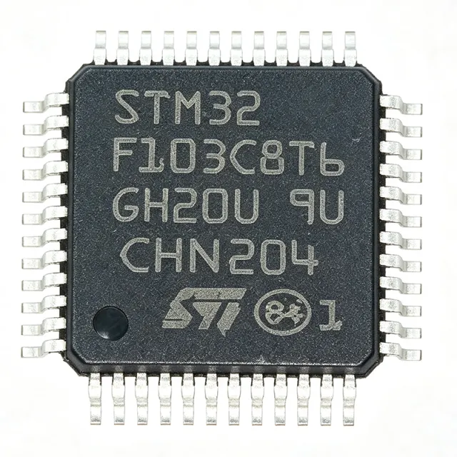
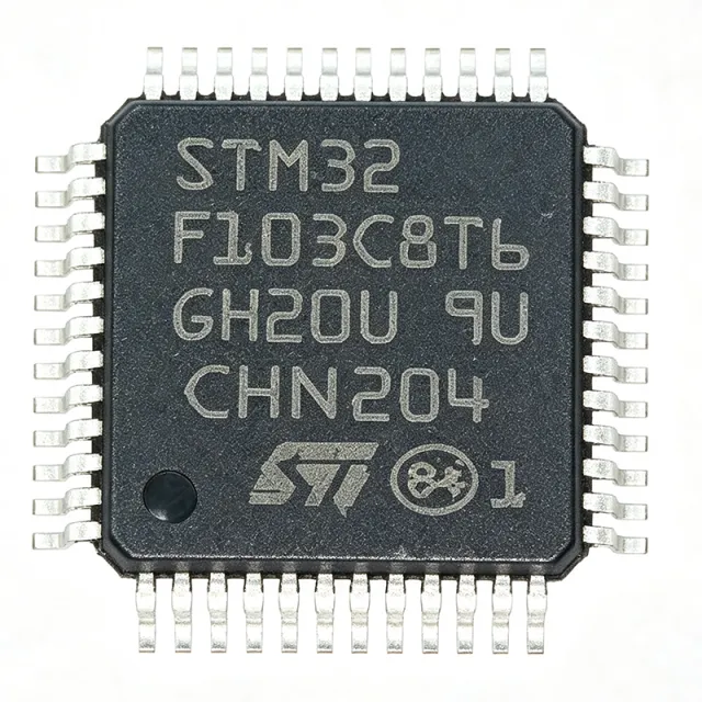
STM32F103C8T6 - 32-bit ARM Cortex-M3 MCU, 64KB Flash | STMicroelectronics
STM32F103C8T6

STM32F103C8T6 - 32-bit ARM Cortex-M3 MCU, 64KB Flash | STMicroelectronics

The STM32F103C8T6 is a 32-bit ARM Cortex-M3 microcontroller from STMicroelectronics, featuring 64KB Flash, 20KB SRAM, and operating at up to 72 MHz. It includes multiple communication interfaces (USART, SPI, I2C, USB, CAN) and 12-bit ADCs, making it suitable for industrial control, motor drives, and IoT applications. Available in LQFP-48 package.

USD $1,02 En stock
STM32F103C8T6 - 72MHz Cortex-M3 MCU, 64KB Flash, LQFP-48 | STMicroelectronics
STM32F103C8T6

STM32F103C8T6 - 72MHz Cortex-M3 MCU, 64KB Flash, LQFP-48 | STMicroelectronics

The STMicroelectronics STM32F103C8T6 is a 32-bit ARM Cortex-M3 medium-density performance-line microcontroller operating at up to 72 MHz, with 64 KB Flash and 20 KB SRAM, housed in a 48-pin LQFP package (7x7 mm). An ARM Cortex-M3 microcontroller (MCU) is a 32-bit RISC processor core designed by Arm Holdings for embedded applications requiring deterministic real-time performance at low power. The Cortex-M3 sits at the lower end of the Cortex-M family (above Cortex-M0/M0+ and below Cortex-M4/M7), and microcontrollers in this category combine the processor core with on-chip memory, peripherals, and analog blocks into a single system-on-chip. The STM32F103 family specifically belongs to the broader hierarchy: ARM Cortex-M3 -> 32-bit MCU -> STM32F1 series -> STM32 mainstream family -> STMicroelectronics microcontrollers -> semiconductor. This hierarchy matters because it determines the toolchain (Arm Cortex-M3 supports the standard Arm Keil, IAR, GCC, and STM32CubeIDE flows) and the peripheral programming model used across the STM32 platform. Key features include 64 KB of embedded Flash with read-while-write capability, 20 KB of SRAM, a 2.0 V to 3.6 V supply range, an 8 MHz internal RC oscillator with PLL multiplier to 72 MHz, two 12-bit ADCs (1 µs conversion, up to 16 channels), seven 16-bit timers, and a full-speed USB 2.0 Full-Speed device/host/OTG controller. Communication peripherals include three USARTs, two SPIs (18 Mbit/s), two I2C buses (400 kHz), one CAN 2.0B interface, and one USB Full-Speed port. The 48-pin LQFP package exposes 37 GPIO pins tolerant to 5 V. Architecturally, the Cortex-M3 core delivers 1.25 Dhrystone MIPS per MHz, supports the Thumb-2 instruction set, and includes a Nested Vectored Interrupt Controller (NVIC) with configurable priority and hardware stack handling. The integrated voltage regulator and brown-out reset (BOR) simplify power design, while the 4-byte backup register with a tamper-detection pin supports battery-backed RTC modes. Typical applications include industrial control boards, motor drives (BLDC/PMSM FOC complements), USB HID/COM port devices, CAN-bus node interfaces, and low-cost development platforms such as the well-known "Blue Pill" board. When designing with this device, place a 100 nF ceramic decoupling capacitor as close as possible to each VDD/VDDA pin pair, and reserve the NRST pin connection for a 10 kΩ pull-up and optional reset button. Ensure the BOOT0 pin state matches the desired boot memory on every power-up. This page synthesizes distributor pricing, drop-in alternatives (same-brand STM32F103 variants first, then cross-brand pin-compatible parts), and practical design notes not found in the manufacturer datasheet.

USD $0,90 En stock
STM32F103C8T6TR - 72MHz Cortex-M3 MCU, 64KB Flash, LQFP-48 | STMicroelectronics (Tape & Reel)
STM32F103C8T6TR

STM32F103C8T6TR - 72MHz Cortex-M3 MCU, 64KB Flash, LQFP-48 | STMicroelectronics (Tape & Reel)

The STMicroelectronics STM32F103C8T6TR is a 32-bit ARM Cortex-M3 medium-density performance-line microcontroller operating at up to 72 MHz, with 64 KB Flash and 20 KB SRAM, housed in a 48-pin LQFP package (7x7 mm). An ARM Cortex-M3 microcontroller (MCU) is a 32-bit RISC processor core designed by Arm Holdings for embedded applications requiring deterministic real-time performance at low power. The Cortex-M3 sits at the lower end of the Cortex-M family (above Cortex-M0/M0+ and below Cortex-M4/M7), and microcontrollers in this category combine the processor core with on-chip memory, peripherals, and analog blocks into a single system-on-chip. The STM32F103 family specifically belongs to the broader hierarchy: ARM Cortex-M3 -> 32-bit MCU -> STM32F1 series -> STM32 mainstream family -> STMicroelectronics microcontrollers -> semiconductor. This hierarchy matters because it determines the toolchain (Arm Cortex-M3 supports the standard Arm Keil, IAR, GCC, and STM32CubeIDE flows) and the peripheral programming model used across the STM32 platform. Key features include 64 KB of embedded Flash with read-while-write capability, 20 KB of SRAM, a 2.0 V to 3.6 V supply range, an 8 MHz internal RC oscillator with PLL multiplier to 72 MHz, two 12-bit ADCs (1 µs conversion, up to 16 channels), seven 16-bit timers, and a full-speed USB 2.0 Full-Speed device/host/OTG controller. Communication peripherals include three USARTs, two SPIs (18 Mbit/s), two I2C buses (400 kHz), one CAN 2.0B interface, and one USB Full-Speed port. The 48-pin LQFP package exposes 37 GPIO pins tolerant to 5 V. Architecturally, the Cortex-M3 core delivers 1.25 Dhrystone MIPS per MHz, supports the Thumb-2 instruction set, and includes a Nested Vectored Interrupt Controller (NVIC) with configurable priority and hardware stack handling. The integrated voltage regulator and brown-out reset (BOR) simplify power design, while the 4-byte backup register with a tamper-detection pin supports battery-backed RTC modes. Typical applications include industrial control boards, motor drives (BLDC/PMSM FOC complements), USB HID/COM port devices, CAN-bus node interfaces, and low-cost development platforms such as the well-known "Blue Pill" board. When designing with this device, place a 100 nF ceramic decoupling capacitor as close as possible to each VDD/VDDA pin pair, and reserve the NRST pin connection for a 10 kΩ pull-up and optional reset button. Ensure the BOOT0 pin state matches the desired boot memory on every power-up. This page synthesizes distributor pricing, drop-in alternatives (same-brand STM32F103 variants first, then cross-brand pin-compatible parts), and practical design notes not found in the manufacturer datasheet.

USD $1,68 En stock
STM32F103C8T7 - 72MHz Cortex-M3 MCU 64KB LQFP-48 | STMicroelectronics
STM32F103C8T7

STM32F103C8T7 - 72MHz Cortex-M3 MCU 64KB LQFP-48 | STMicroelectronics

The STMicroelectronics STM32F103C8T7 is a medium-density performance-line ARM Cortex-M3 microcontroller operating at 72 MHz with 64 KB of Flash and 20 KB of SRAM, housed in a 48-pin LQFP (7x7 mm) package. It integrates USB 2.0 Full-Speed, CAN 2.0B, seven 16-bit timers, two 12-bit ADCs (up to 1 MSPS), and nine communication interfaces (I2C, SPI, USART, USB, CAN) on a single die, delivering 90 DMIPS at 1.25 DMIPS/MHz. An ARM Cortex-M3 microcontroller is a 32-bit RISC processor core designed for deterministic real-time embedded control, sitting within a broader taxonomy of MCU -> embedded processor -> microcontroller -> semiconductor. Cortex-M3 cores specifically target low-latency interrupt response (typically 12 clock cycles), Thumb-2 instruction efficiency, and hardware divide in a small footprint, making them the workhorse of industrial motor control, USB peripherals, and consumer device controllers where deterministic behavior matters more than raw clock speed. Key features include 72 MHz CPU with hardware single-cycle multiply, 64 KB Flash with read-while-write support, 20 KB SRAM, a 12-bit ADC with up to 10 channels, two I2C, two SPI, three USART, one USB Full-Speed, and one CAN 2.0B interface. Operating voltage spans 2.0V to 3.6V with internal 8 MHz and 40 kHz RC oscillators plus a PLL multiplying up to 72 MHz. The architecture pairs the Cortex-M3 core with a Nested Vectored Interrupt Controller (NVIC) supporting up to 43 maskable interrupts, a DMA controller with seven channels, and a power management block offering Sleep, Stop, and Standby modes. The bus matrix arbitrates between the core, DMA, and peripherals to keep deterministic throughput even when USB or CAN packets arrive. Typical applications include USB HID peripherals, industrial CAN-bus nodes, motor-control boards, low-cost development platforms (the 'Blue Pill' form factor), and consumer device controllers. The integrated USB PHY and CAN 2.0B controller make it particularly suited for bridging PC and industrial networks without external transceiver logic. Operating temperature spans -40C to +105C for the industrial grade. When designing with this device, watch the 2.0V minimum VDD during PLL start-up and ensure decoupling comprises a 100 nF X7R per VDD pin plus a bulk 4.7 uF tantalum or ceramic. The NRST pin requires an external 10 kohm pull-up and a 100 nF capacitor to VDD for reliable reset. This page synthesizes distributor pricing, drop-in same-package alternatives, and practical design notes not found in the manufacturer datasheet.

Devis Contact
STM32F103C8T7TR - 72MHz Cortex-M3 MCU 64KB LQFP-48 | STMicroelectronics (Tape & Reel)
STM32F103C8T7TR

STM32F103C8T7TR - 72MHz Cortex-M3 MCU 64KB LQFP-48 | STMicroelectronics (Tape & Reel)

The STMicroelectronics STM32F103C8T7TR is a medium-density performance-line ARM Cortex-M3 microcontroller operating at 72 MHz with 64 KB of Flash and 20 KB of SRAM, housed in a 48-pin LQFP (7x7 mm) package. It integrates USB 2.0 Full-Speed, CAN 2.0B, seven 16-bit timers, two 12-bit ADCs (up to 1 MSPS), and nine communication interfaces (I2C, SPI, USART, USB, CAN) on a single die, delivering 90 DMIPS at 1.25 DMIPS/MHz. An ARM Cortex-M3 microcontroller is a 32-bit RISC processor core designed for deterministic real-time embedded control, sitting within a broader taxonomy of MCU -> embedded processor -> microcontroller -> semiconductor. Cortex-M3 cores specifically target low-latency interrupt response (typically 12 clock cycles), Thumb-2 instruction efficiency, and hardware divide in a small footprint, making them the workhorse of industrial motor control, USB peripherals, and consumer device controllers where deterministic behavior matters more than raw clock speed. Key features include 72 MHz CPU with hardware single-cycle multiply, 64 KB Flash with read-while-write support, 20 KB SRAM, a 12-bit ADC with up to 10 channels, two I2C, two SPI, three USART, one USB Full-Speed, and one CAN 2.0B interface. Operating voltage spans 2.0V to 3.6V with internal 8 MHz and 40 kHz RC oscillators plus a PLL multiplying up to 72 MHz. The architecture pairs the Cortex-M3 core with a Nested Vectored Interrupt Controller (NVIC) supporting up to 43 maskable interrupts, a DMA controller with seven channels, and a power management block offering Sleep, Stop, and Standby modes. The bus matrix arbitrates between the core, DMA, and peripherals to keep deterministic throughput even when USB or CAN packets arrive. Typical applications include USB HID peripherals, industrial CAN-bus nodes, motor-control boards, low-cost development platforms (the 'Blue Pill' form factor), and consumer device controllers. The integrated USB PHY and CAN 2.0B controller make it particularly suited for bridging PC and industrial networks without external transceiver logic. Operating temperature spans -40C to +105C for the industrial grade. When designing with this device, watch the 2.0V minimum VDD during PLL start-up and ensure decoupling comprises a 100 nF X7R per VDD pin plus a bulk 4.7 uF tantalum or ceramic. The NRST pin requires an external 10 kohm pull-up and a 100 nF capacitor to VDD for reliable reset. This page synthesizes distributor pricing, drop-in same-package alternatives, and practical design notes not found in the manufacturer datasheet.

Devis Contact
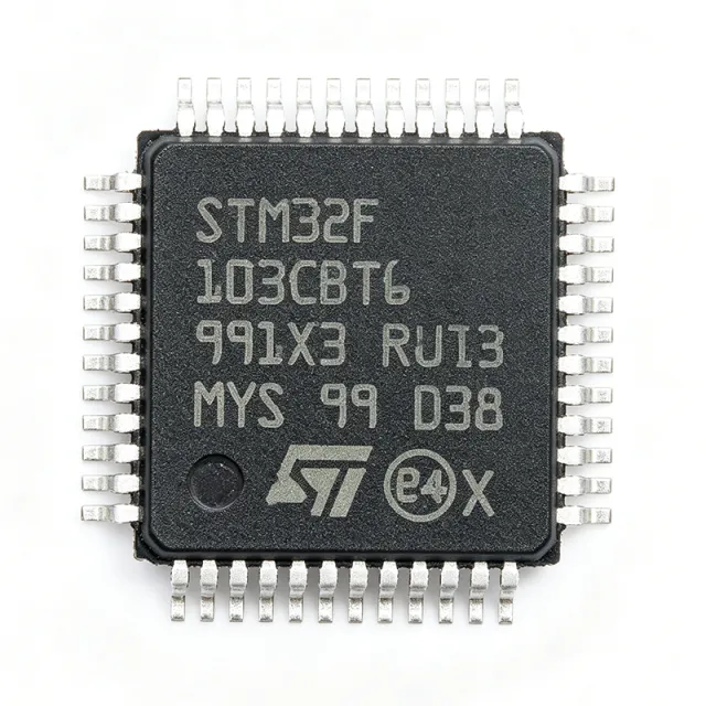
STM32F103CBT6 - 72MHz Cortex-M3 128KB Flash MCU | STMicroelectronics
STM32F103CBT6

STM32F103CBT6 - 72MHz Cortex-M3 128KB Flash MCU | STMicroelectronics

The STMicroelectronics STM32F103CBT6 is a 32-bit ARM Cortex-M3 mainstream microcontroller running at up to 72 MHz with 128 KB of Flash and 20 KB of SRAM, packaged in a 48-pin LQFP (7x7 mm) device. What is a microcontroller? An MCU integrates a processor core, on-chip non-volatile memory (Flash), volatile working memory (SRAM), and a set of programmable peripherals onto a single silicon die. Within the embedded-computing hierarchy it sits above a bare microprocessor and below a full system-on-chip, and within ST's own portfolio the STM32F1 mainstream series places the STM32F103CBT6 between the ultra-low-power STM32L family and the higher-performance Cortex-M4 STM32F4 family. The part belongs to the medium-density STM32F103xx performance line, which targets cost-sensitive industrial and consumer control. Key features include a 72 MHz Cortex-M3 core with single-cycle hardware multiply and divide, a 2.0 V to 3.6 V supply range, an embedded nested vectored interrupt controller with 43 maskable channels, and up to 37 GPIO pins tolerant to 5 V. On-board communication is broad for the class: three USARTs, two I2C buses, two SPI interfaces, one full-speed USB 2.0 device port, and one CAN 2.0B active controller. Two 12-bit ADCs (1 us conversion), one 12-bit DAC, three general-purpose 16-bit timers, one PWM timer, and one basic timer give ample motor-control flexibility. Technically, the clock tree uses an internal 8 MHz RC oscillator plus a 4-16 MHz external crystal and a dedicated 32 kHz RTC oscillator; PLL multiplication reaches 72 MHz. Programming is via SWD or JTAG, with a built-in bootloader selectable via BOOT0/BOOT1. The 7x7 mm LQFP-48 package gives a low-cost, easy-to-assemble footprint suitable for both hand-soldered prototypes and high-volume SMT lines. Typical applications include industrial control nodes, motor drives, USB-to-CAN fieldbus bridges, medical instruments, smart-home hubs, and IoT gateways, where the combination of USB, CAN, and multiple UARTs positions the part as a communication-rich embedded hub. For design, decouple every VDD pin with 100 nF ceramics plus a single 4.7 uF bulk, place the HSE crystal traces short and guarded, and tie BOOT0 to GND for normal Flash boot or to VDD for system-memory bootloader. This page synthesises distributor pricing, drop-in alternatives (GD32F103CBT6, APM32F103CBT6, AT32F403ACBT7), and practical design notes not found in the ST datasheet.

USD $3,20 Contact
STM32F103CBT6TR - 72MHz Cortex-M3 128KB Flash MCU | STMicroelectronics (Tape & Reel)
STM32F103CBT6TR

STM32F103CBT6TR - 72MHz Cortex-M3 128KB Flash MCU | STMicroelectronics (Tape & Reel)

The STMicroelectronics STM32F103CBT6TR is a 32-bit ARM Cortex-M3 mainstream microcontroller running at up to 72 MHz with 128 KB of Flash and 20 KB of SRAM, packaged in a 48-pin LQFP (7x7 mm) device. What is a microcontroller? An MCU integrates a processor core, on-chip non-volatile memory (Flash), volatile working memory (SRAM), and a set of programmable peripherals onto a single silicon die. Within the embedded-computing hierarchy it sits above a bare microprocessor and below a full system-on-chip, and within ST's own portfolio the STM32F1 mainstream series places the STM32F103CBT6TR between the ultra-low-power STM32L family and the higher-performance Cortex-M4 STM32F4 family. The part belongs to the medium-density STM32F103xx performance line, which targets cost-sensitive industrial and consumer control. Key features include a 72 MHz Cortex-M3 core with single-cycle hardware multiply and divide, a 2.0 V to 3.6 V supply range, an embedded nested vectored interrupt controller with 43 maskable channels, and up to 37 GPIO pins tolerant to 5 V. On-board communication is broad for the class: three USARTs, two I2C buses, two SPI interfaces, one full-speed USB 2.0 device port, and one CAN 2.0B active controller. Two 12-bit ADCs (1 us conversion), one 12-bit DAC, three general-purpose 16-bit timers, one PWM timer, and one basic timer give ample motor-control flexibility. Technically, the clock tree uses an internal 8 MHz RC oscillator plus a 4-16 MHz external crystal and a dedicated 32 kHz RTC oscillator; PLL multiplication reaches 72 MHz. Programming is via SWD or JTAG, with a built-in bootloader selectable via BOOT0/BOOT1. The 7x7 mm LQFP-48 package gives a low-cost, easy-to-assemble footprint suitable for both hand-soldered prototypes and high-volume SMT lines. Typical applications include industrial control nodes, motor drives, USB-to-CAN fieldbus bridges, medical instruments, smart-home hubs, and IoT gateways, where the combination of USB, CAN, and multiple UARTs positions the part as a communication-rich embedded hub. For design, decouple every VDD pin with 100 nF ceramics plus a single 4.7 uF bulk, place the HSE crystal traces short and guarded, and tie BOOT0 to GND for normal Flash boot or to VDD for system-memory bootloader. This page synthesises distributor pricing, drop-in alternatives (GD32F103CBT6, APM32F103CBT6, AT32F403ACBT7), and practical design notes not found in the ST datasheet.

USD $3,20 Contact
STM32F103CBT7 - 72MHz Cortex-M3 128KB MCU | STMicroelectronics
STM32F103CBT7

STM32F103CBT7 - 72MHz Cortex-M3 128KB MCU | STMicroelectronics

The STMicroelectronics STM32F103CBT7 is a 32-bit ARM Cortex-M3 microcontroller operating at up to 72MHz, with 128KB of flash memory and a 48-LQFP 7x7mm package. It is designed for embedded control applications requiring real-time processing, serial connectivity, timers, and mixed peripherals. The verified distributor data identifies the part as an STM32F1 microcontroller with 128KB flash and a 48-LQFP package. A microcontroller is a semiconductor that integrates a processor core, memory, and peripherals into one programmable device. The STM32F1 family belongs to the ARM Cortex-M embedded ecosystem, where the MCU executes firmware from flash and uses peripherals to interface with sensors, communication networks, motors, displays, and control systems. STM32F103CBT7 is specifically associated with the medium-density performance line and is suitable for designs where a Cortex-M3 core and compact 48-pin implementation are required. The key verified characteristics are a 32-bit Cortex-M3 processor, 72MHz maximum operating frequency, 128KB flash, and a 48-LQFP 7x7mm package. These values make the device appropriate for industrial controllers, communication modules, motor-control peripherals, instrument interfaces, and embedded automation products. The LQFP package also provides a practical surface-mount format for prototypes and medium-density production assemblies. The STM32F103CBT7 is a programmable embedded platform rather than a fixed-function controller. Firmware determines the behavior of its GPIO, timers, serial interfaces, analog functions, and interrupt-driven control loops. Designers should therefore validate the complete peripheral configuration, clock plan, memory usage, and board-level power requirements against the applicable STMicroelectronics documentation before production release. Typical applications include connected industrial sensors, compact motor-control boards, USB or UART communication modules, data acquisition equipment, and embedded controller platforms. The 72MHz Cortex-M3 core provides processing headroom for control tasks, while 128KB flash provides room for application code and bootloader logic. The 48-LQFP package remains useful where a moderate pin count and easy visual inspection are preferred over a very small package. When designing around STM32F103CBT7, preserve the required decoupling and oscillator layout recommended by the manufacturer documentation, and confirm the exact peripheral pin mapping for the selected board. Do not assume that a competitor with a similar package name is electrically or firmware compatible without checking pin functions, voltage limits, clock behavior, and peripheral differences. This page combines verified distributor data with clearly marked data gaps rather than estimating missing electrical details. This product reference is intended to help engineers identify the correct MCU, compare possible replacements, and plan an embedded design. The most important engineering checks are package compatibility, firmware portability, peripheral coverage, clock configuration, and supply availability.

Devis Contact
STM32F103CBT7TR - 72MHz Cortex-M3 128KB MCU | STMicroelectronics (Tape & Reel)
STM32F103CBT7TR

STM32F103CBT7TR - 72MHz Cortex-M3 128KB MCU | STMicroelectronics (Tape & Reel)

The STMicroelectronics STM32F103CBT7TR is a 32-bit ARM Cortex-M3 microcontroller operating at up to 72MHz, with 128KB of flash memory and a 48-LQFP 7x7mm package. It is designed for embedded control applications requiring real-time processing, serial connectivity, timers, and mixed peripherals. The verified distributor data identifies the part as an STM32F1 microcontroller with 128KB flash and a 48-LQFP package. A microcontroller is a semiconductor that integrates a processor core, memory, and peripherals into one programmable device. The STM32F1 family belongs to the ARM Cortex-M embedded ecosystem, where the MCU executes firmware from flash and uses peripherals to interface with sensors, communication networks, motors, displays, and control systems. STM32F103CBT7TR is specifically associated with the medium-density performance line and is suitable for designs where a Cortex-M3 core and compact 48-pin implementation are required. The key verified characteristics are a 32-bit Cortex-M3 processor, 72MHz maximum operating frequency, 128KB flash, and a 48-LQFP 7x7mm package. These values make the device appropriate for industrial controllers, communication modules, motor-control peripherals, instrument interfaces, and embedded automation products. The LQFP package also provides a practical surface-mount format for prototypes and medium-density production assemblies. The STM32F103CBT7TR is a programmable embedded platform rather than a fixed-function controller. Firmware determines the behavior of its GPIO, timers, serial interfaces, analog functions, and interrupt-driven control loops. Designers should therefore validate the complete peripheral configuration, clock plan, memory usage, and board-level power requirements against the applicable STMicroelectronics documentation before production release. Typical applications include connected industrial sensors, compact motor-control boards, USB or UART communication modules, data acquisition equipment, and embedded controller platforms. The 72MHz Cortex-M3 core provides processing headroom for control tasks, while 128KB flash provides room for application code and bootloader logic. The 48-LQFP package remains useful where a moderate pin count and easy visual inspection are preferred over a very small package. When designing around STM32F103CBT7TR, preserve the required decoupling and oscillator layout recommended by the manufacturer documentation, and confirm the exact peripheral pin mapping for the selected board. Do not assume that a competitor with a similar package name is electrically or firmware compatible without checking pin functions, voltage limits, clock behavior, and peripheral differences. This page combines verified distributor data with clearly marked data gaps rather than estimating missing electrical details. This product reference is intended to help engineers identify the correct MCU, compare possible replacements, and plan an embedded design. The most important engineering checks are package compatibility, firmware portability, peripheral coverage, clock configuration, and supply availability.

Devis Contact
STM32F103CBU6 - 72MHz Cortex-M3 128KB MCU | STMicroelectronics
STM32F103CBU6

STM32F103CBU6 - 72MHz Cortex-M3 128KB MCU | STMicroelectronics

The STMicroelectronics STM32F103CBU6 is a 32-bit ARM Cortex-M3 microcontroller operating up to 72 MHz, with 128 KB of Flash memory and a 48-pin UFQFPN package measuring 7 mm by 7 mm. The verified distributor listing identifies this part as an STM32F1 performance-line MCU with 128K x 8 Flash organization. It combines general-purpose embedded processing with USB, CAN, timers, ADCs, and multiple communication interfaces in one compact surface-mount device. A microcontroller is a programmable semiconductor that integrates a CPU core, memory, peripherals, and interfaces into a single embedded-control component. The STM32F103 belongs to the ARM Cortex-M microcontroller class and the broader embedded-processor hierarchy: MCU, microcontroller, embedded processor, and semiconductor. This device family is intended for systems that need deterministic control, serial communications, analog measurement, and moderate firmware complexity without a separate processor. Key verified features include a 72 MHz ARM Cortex-M3 CPU, 1.25 DMIPS/MHz Dhrystone 2.1 performance at zero-wait-state memory access, single-cycle multiplication, hardware division, and 128 KB of Flash. The family feature description also identifies USB, CAN, seven timers, two ADCs, and nine communication interfaces. These peripherals support connected industrial controls, USB peripherals, CAN nodes, measurement systems, and compact embedded products. The STM32F103CBU6 uses a 48-UFQFPN package with an exposed pad, enabling a compact PCB footprint and improved heat spreading when the pad is properly connected to the ground plane. The MCU is not a power semiconductor, so a safe-operating-area chart is not applicable. Supply voltage, current, temperature limits, pin functions, and detailed electrical limits are not fully included in the supplied verified data and must be confirmed from the manufacturer datasheet before design release. Typical applications include industrial automation, USB-enabled embedded controls, CAN-connected equipment, motor and motor-control systems, instrumentation, and low-cost development platforms. Its 72 MHz processing rate and communication peripherals make it suitable for control loops that require more performance than a simple 8-bit MCU while retaining a broad embedded peripheral set. The 48-pin package also offers more I/O and interface options than smaller 32-pin or 20-pin devices. For a new design, preserve the exposed-pad land pattern, follow the manufacturer's decoupling and layout guidance, and verify pin multiplexing, clock configuration, peripheral assignment, and firmware support against the exact datasheet and reference manual. This page combines verified distributor specifications, sourced replacement information, comparison structure, and practical design guidance; it does not substitute for an electrical sign-off of the manufacturer documentation.

Devis Contact
STM32F103CBU6TR - 72MHz Cortex-M3 128KB MCU | STMicroelectronics (Tape & Reel)
STM32F103CBU6TR

STM32F103CBU6TR - 72MHz Cortex-M3 128KB MCU | STMicroelectronics (Tape & Reel)

The STMicroelectronics STM32F103CBU6TR is a 32-bit ARM Cortex-M3 microcontroller operating up to 72 MHz, with 128 KB of Flash memory and a 48-pin UFQFPN package measuring 7 mm by 7 mm. The verified distributor listing identifies this part as an STM32F1 performance-line MCU with 128K x 8 Flash organization. It combines general-purpose embedded processing with USB, CAN, timers, ADCs, and multiple communication interfaces in one compact surface-mount device. A microcontroller is a programmable semiconductor that integrates a CPU core, memory, peripherals, and interfaces into a single embedded-control component. The STM32F103 belongs to the ARM Cortex-M microcontroller class and the broader embedded-processor hierarchy: MCU, microcontroller, embedded processor, and semiconductor. This device family is intended for systems that need deterministic control, serial communications, analog measurement, and moderate firmware complexity without a separate processor. Key verified features include a 72 MHz ARM Cortex-M3 CPU, 1.25 DMIPS/MHz Dhrystone 2.1 performance at zero-wait-state memory access, single-cycle multiplication, hardware division, and 128 KB of Flash. The family feature description also identifies USB, CAN, seven timers, two ADCs, and nine communication interfaces. These peripherals support connected industrial controls, USB peripherals, CAN nodes, measurement systems, and compact embedded products. The STM32F103CBU6TR uses a 48-UFQFPN package with an exposed pad, enabling a compact PCB footprint and improved heat spreading when the pad is properly connected to the ground plane. The MCU is not a power semiconductor, so a safe-operating-area chart is not applicable. Supply voltage, current, temperature limits, pin functions, and detailed electrical limits are not fully included in the supplied verified data and must be confirmed from the manufacturer datasheet before design release. Typical applications include industrial automation, USB-enabled embedded controls, CAN-connected equipment, motor and motor-control systems, instrumentation, and low-cost development platforms. Its 72 MHz processing rate and communication peripherals make it suitable for control loops that require more performance than a simple 8-bit MCU while retaining a broad embedded peripheral set. The 48-pin package also offers more I/O and interface options than smaller 32-pin or 20-pin devices. For a new design, preserve the exposed-pad land pattern, follow the manufacturer's decoupling and layout guidance, and verify pin multiplexing, clock configuration, peripheral assignment, and firmware support against the exact datasheet and reference manual. This page combines verified distributor specifications, sourced replacement information, comparison structure, and practical design guidance; it does not substitute for an electrical sign-off of the manufacturer documentation.

Devis Contact
STM32F103R4H6A - 72MHz ARM Cortex-M3 MCU | STMicroelectronics
STM32F103R4H6A

STM32F103R4H6A - 72MHz ARM Cortex-M3 MCU | STMicroelectronics

The STMicroelectronics STM32F103R4H6A is a 32-bit ARM Cortex-M3 microcontroller operating at up to 72 MHz, with 16 KB of Flash memory and 64-pin TFBGA packaging in a 5 x 5 mm footprint. It combines a 2.0 V to 3.6 V supply range with 37 I/O ports and belongs to the STM32F103 low-density performance line. The device is positioned for compact embedded-control systems requiring USB, CAN, timers, analog conversion, and multiple communication interfaces without the memory footprint of a high-density STM32 design. A microcontroller is an integrated circuit that combines a processor core, memory, peripherals, and I/O in one device. The ARM Cortex-M3 core provides deterministic embedded processing, while the STM32F103 family adds timers, communication interfaces, analog converters, and GPIO resources. In the product hierarchy, this component is an MCU, a semiconductor, and a member of the STM32F1 low-density performance line. Key features include a maximum CPU frequency of 72 MHz, 16 KB of Flash, and 37 I/O ports. The verified product listing also identifies USB, CAN, six timers, two ADCs, and six communication interfaces within the applicable STM32F103 low-density family. These resources support USB-connected peripherals, CAN-based industrial or automotive communication, periodic control functions, and analog sensor acquisition. A separate source identifies a 2 V to 3.6 V supply range and RoHS-compliant construction, although exact operating-temperature and electrical-limit details were not included in the supplied data. The Cortex-M3 architecture supports 32-bit instruction execution and efficient embedded control without an external memory interface being required for the stated 16 KB configuration. Its peripherals reduce the need for discrete interface components in designs that combine data acquisition, communications, and control functions. Package density also makes the 5 x 5 mm TFBGA useful for compact modules and densely populated industrial controllers, although it requires careful PCB layout and inspection because its leads are hidden beneath the package. Typical uses include USB data acquisition equipment, CAN-connected industrial controls, motor-control subsystems, communication adapters, and compact embedded-control modules. The STM32F103R4H6A is especially appropriate when a design needs several peripherals but only 16 KB of application Flash. Developers should confirm that code size, firmware requirements, peripheral configuration, and production availability remain within the device's limits before final release. A primary design consideration is BGA assembly. Its pads require via-in-pad or fanout-capable PCB construction, adequate solder-paste control, X-ray inspection, and careful power-and-ground plane design. Decoupling should be placed directly at the appropriate supply pins, while signal routing must preserve USB, CAN, clock, and analog-input signal integrity. Confirming the exact pinout against the manufacturer datasheet is mandatory because the supplied sources do not provide the complete numbered 64-pin assignment. This page consolidates verified distributor and manufacturer information, strict same-package replacement candidates, application guidance, and practical PCB considerations. It distinguishes confirmed parameters from values that still require datasheet confirmation so engineers can make sourcing and design decisions without unsupported assumptions.

Devis Contact
STM32F103R4T6A - 72MHz Cortex-M3 16KB MCU | STMicroelectronics
STM32F103R4T6A

STM32F103R4T6A - 72MHz Cortex-M3 16KB MCU | STMicroelectronics

STMicroelectronics STM32F103R4T6A is an ARM Cortex-M3 32-bit RISC microcontroller with a 72 MHz maximum operating frequency, 16 KB of Flash program memory, and a 64-pin LQFP package. The device belongs to the STM32F103x4 low-density performance line and is positioned for compact embedded-control, communication, analog-interface, and USB applications. A microcontroller is a programmable semiconductor that integrates a processor core, memory, peripheral interfaces, and control logic into one device. The STM32F103 family combines an ARM Cortex-M3 CPU with Flash memory, SRAM, timers, communication peripherals, and analog conversion resources. This integration lets an embedded product execute application firmware, acquire sensor data, control outputs, and exchange information without requiring several separate devices. The STM32F103R4T6A provides 16 KB of Flash memory and operates at up to 72 MHz. Its documented feature set includes USB, CAN, six timers, two ADCs, and six communication interfaces. These resources support designs that need moderate processing performance and multiple peripheral functions within a constrained board area. The 64-pin LQFP package also exposes a comparatively broad set of GPIO and interface options. The ARM Cortex-M3 core uses a 32-bit RISC architecture and is designed for efficient real-time control. Its instruction set supports interrupt-driven operation, while the STM32 peripheral set connects timers to motor-control and timing tasks, ADCs to analog measurement, and serial interfaces to communications networks. The 1.25 DMIPS/MHz performance figure quoted for the STM32F103 family illustrates its processing efficiency, although final application performance depends on firmware and system configuration. Typical uses include USB-connected data acquisition, CAN-based industrial or automotive equipment, motor-control systems, sensor nodes, and compact embedded controllers. The two ADCs support analog measurement, the timers support precise event and waveform generation, and USB or CAN provides a path for data exchange. Firmware and peripheral configuration must be checked against the selected device variant because STM32 families can contain parts with different memory capacities and feature combinations. Place decoupling capacitors close to the power and ground pins, preserve the manufacturer's recommended clock and reset arrangements, and route high-frequency or sensitive analog signals away from switching nodes. Because the exact pin assignments and electrical limits are defined by the manufacturer documentation, use the STM32F103x4 reference manual and pin-description tables when assigning PCB tracks. This product page combines the exact STM32F103R4T6A identity, memory, frequency, package, interface, and lifecycle information with sourcing guidance, documented drop-in candidates, comparison criteria, and practical embedded-design considerations. Request current availability, lead time, and commercial terms through the Request a Quote form on this page.

Devis Contact