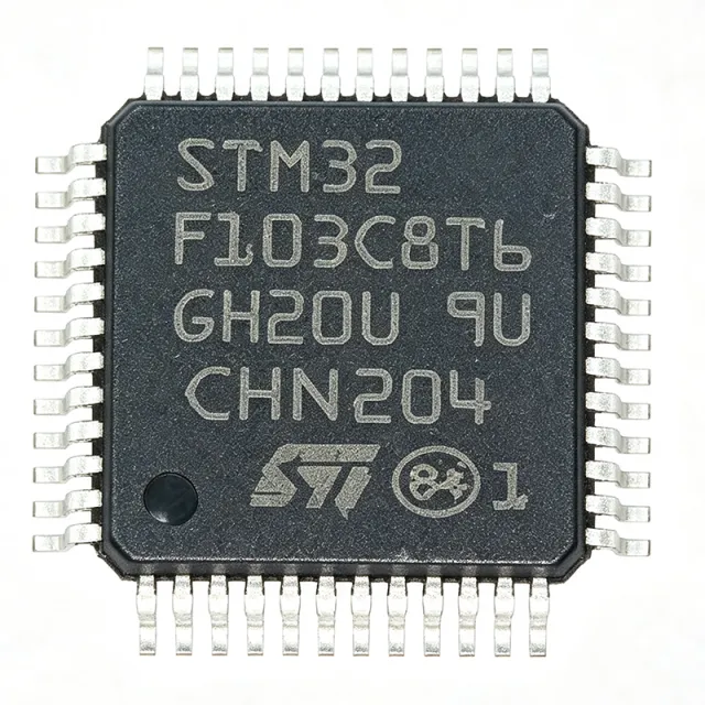
STM32F103C8T6 - MCU Cortex-M3 72 MHz, 64 Ko de Flash, LQFP-48 | STMicroelectronics
Référence : STM32F103C8T6 ✓ Actif| Qté | Prix unitaire | Total |
|---|---|---|
| 1 | $3.1 | $3,10 |
| 10 | $2.78 | $27,80 |
| 100 | $2.45 | $245,00 |
| 500 | $2.18 | $1 090,00 |
| 1 000 | $1.92 | $1 920,00 |
| 3 000 | $1.68 | $5 040,00 |
STM32F103C8T6 Présentation
Un microcontrôleur (MCU) ARM Cortex-M3 est un cœur de processeur RISC 32 bits conçu par Arm Holdings pour les applications embarquées nécessitant des performances temps réel déterministes à faible consommation. Le Cortex-M3 se situe dans la partie basse de la famille Cortex-M (au-dessus des Cortex-M0/M0+ et en dessous des Cortex-M4/M7), et les microcontrôleurs de cette catégorie combinent le cœur du processeur avec la mémoire embarquée, les périphériques et les blocs analogiques dans un seul système sur puce. La famille STM32F103 appartient spécifiquement à la hiérarchie plus large : ARM Cortex-M3 -> MCU 32 bits -> série STM32F1 -> famille grand public STM32 -> microcontrôleurs STMicroelectronics -> semi-conducteur. Cette hiérarchie est importante car elle détermine la chaîne d'outils (Arm Cortex-M3 prend en charge les flux standard Arm Keil, IAR, GCC et STM32CubeIDE) et le modèle de programmation des périphériques utilisé sur toute la plateforme STM32.
Les principales caractéristiques comprennent 64 Ko de Flash embarquée avec capacité de lecture pendant écriture, 20 Ko de SRAM, une plage d'alimentation de 2,0 V à 3,6 V, un oscillateur RC interne de 8 MHz avec multiplicateur PLL jusqu'à 72 MHz, deux CAN 12 bits (conversion 1 µs, jusqu'à 16 canaux), sept temporisateurs 16 bits et un contrôleur USB 2.0 Full-Speed device/host/OTG. Les périphériques de communication comprennent trois USART, deux SPI (18 Mbit/s), deux bus I2C (400 kHz), une interface CAN 2.0B et un port USB Full-Speed. Le boîtier LQFP à 48 broches expose 37 broches GPIO tolérantes 5 V.
Sur le plan architectural, le cœur Cortex-M3 offre 1,25 Dhrystone MIPS par MHz, prend en charge le jeu d'instructions Thumb-2 et inclut un contrôleur d'interruptions vectorielles imbriquées (NVIC) avec priorité configurable et gestion matérielle de la pile. Le régulateur de tension intégré et la réinitialisation en cas de chute de tension (BOR) simplifient la conception de l'alimentation, tandis que le registre de sauvegarde de 4 octets avec une broche de détection d'effraction prend en charge les modes RTC sauvegardés par batterie.
Les applications typiques comprennent les cartes de contrôle industriel, les entraînements de moteur (compléments BLDC/PMSM FOC), les périphériques USB HID/port COM, les interfaces de nœud de bus CAN et les plateformes de développement à faible coût telles que la célèbre carte « Blue Pill ».
Lors de la conception avec ce composant, placez un condensateur de découplage céramique de 100 nF aussi près que possible de chaque paire de broches VDD/VDDA, et réservez la connexion de la broche NRST pour une résistance de tirage de 10 kΩ et un bouton de réinitialisation optionnel. Assurez-vous que l'état de la broche BOOT0 correspond à la mémoire de démarrage souhaitée à chaque mise sous tension.
Cette page synthétise les prix des distributeurs, les alternatives de remplacement direct (d'abord les variantes STM32F103 de même marque, puis les pièces compatibles broche à broche d'autres marques) et des notes de conception pratiques introuvables dans la fiche technique du fabricant.
Alternatives de remplacement direct pour STM32F103C8T6 — même boîtier, compatible broche à broche. Les références à boîtier différent nécessitant une retouche du PCB sont exclues.
Outil de comparaison rapide — sélectionnez des références alternatives pour une comparaison côte à côte :
STM32F103CBT6
✓ En stock
$3.2 / unité
Voir la fiche technique →STM32F030C8T6
✓ En stock
$0.98 / unité
Voir la fiche technique →STM32F103C8T7
📋 Alternative de référence (hors catalogue)
GD32F103C8T6
📋 Alternative de référence (hors catalogue)
APM32F103C8T6
📋 Alternative de référence (hors catalogue)
STM32F103C8T6 Valeurs maximales et caractéristiques électriques
| Core Architecture | ARM Cortex-M3 (32-bit RISC) |
| Fréquence d'horloge maximale | 72 MHz |
| Flash Memory | 64 KB |
| SRAM | 20 KB |
| Supply Voltage (VDD) | 2.0 V to 3.6 V |
| Boîtier | LQFP-48 (7x7 mm, 0.5 mm pitch) |
| GPIO Count | 37 |
| ADC | 2x 12-bit, 1 µs, up to 16 channels |
| Timers | 7x 16-bit (including 1x watchdog, 2x SysTick) |
| USART | 3 |
| SPI | 2 (18 Mbit/s) |
| I2C | 2 (400 kHz) |
| USB | 1x USB 2.0 Full-Speed device/host/OTG |
| CAN | 1x CAN 2.0B |
| Température de fonctionnement | -40 °C to +85 °C (industrial grade) |
| Statut RoHS | Compliant |
Configuration des broches de STM32F103C8T6
| Broche 1 | VBAT — Backup battery supply input |
| Broche 2 | PC13 — GPIO PC13, anti-tamper (RTC) |
| Broche 3 | PC14 — GPIO PC14 / OSC32_IN |
| Broche 4 | PC15 — GPIO PC15 / OSC32_OUT |
| Broche 5 | OSC_IN — HSE oscillator input |
| Broche 6 | OSC_OUT — HSE oscillator output |
| Broche 7 | NRST — Reset input, active-low |
| Broche 8 | VSSA — Analog ground |
| Broche 9 | VDDA — Analog supply (2.4 V - 3.6 V) |
| Broche 10 | PA0 — GPIO PA0 / WKUP / ADC_IN0 / TIM2_CH1 |
| Broche 11 | PA1 — GPIO PA1 / ADC_IN1 / TIM2_CH2 |
| Broche 12 | PA2 — GPIO PA2 / USART2_TX / ADC_IN2 |
| Broche 13 | PA3 — GPIO PA3 / USART2_RX / ADC_IN3 |
| Broche 14 | PA4 — GPIO PA4 / SPI1_NSS / ADC_IN4 |
| Broche 15 | PA5 — GPIO PA5 / SPI1_SCK / ADC_IN5 |
| Broche 16 | PA6 — GPIO PA6 / SPI1_MISO / ADC_IN6 |
| Broche 17 | PA7 — GPIO PA7 / SPI1_MOSI / ADC_IN7 |
| Broche 18 | PB0 — GPIO PB0 / ADC_IN8 / TIM3_CH3 |
| Broche 19 | PB1 — GPIO PB1 / ADC_IN9 / TIM3_CH4 |
| Broche 20 | PB2 — GPIO PB2 / BOOT1 (also PB-BOOT input) |
| Broche 21 | PB10 — GPIO PB10 / I2C2_SCL / USART3_TX |
| Broche 22 | PB11 — GPIO PB11 / I2C2_SDA / USART3_RX |
| Broche 23 | VSS_1 — Digital ground |
| Broche 24 | VDD_1 — Digital supply (2.0 V - 3.6 V) |
| Broche 25 | PB12 — GPIO PB12 / SPI2_NSS / CAN2_RX |
| Broche 26 | PB13 — GPIO PB13 / SPI2_SCK / CAN2_TX / USB_DP pull-up |
| Broche 27 | PB14 — GPIO PB14 / SPI2_MISO |
| Broche 28 | PB15 — GPIO PB15 / SPI2_MOSI |
| Broche 29 | PA8 — GPIO PA8 / USART1_CK / TIM1_CH1 |
| Broche 30 | PA9 — GPIO PA9 / USART1_TX / TIM1_CH2 |
| Broche 31 | PA10 — GPIO PA10 / USART1_RX / TIM1_CH3 |
| Broche 32 | PA11 — GPIO PA11 / CAN1_RX / USBDM (USB data minus) |
| Broche 33 | PA12 — GPIO PA12 / CAN1_TX / USBDP (USB data plus) |
| Broche 34 | PA13 — GPIO PA13 / JTMS / SWDIO |
| Broche 35 | VSS_2 — Digital ground |
| Broche 36 | VDD_2 — Digital supply (2.0 V - 3.6 V) |
| Broche 37 | PA14 — GPIO PA14 / JTCK / SWCLK |
| Broche 38 | PA15 — GPIO PA15 / JTDI |
| Broche 39 | PB3 — GPIO PB3 / JTDO / TRACESWO |
| Broche 40 | PB4 — GPIO PB4 / JNTRST |
| Broche 41 | PB5 — GPIO PB5 / I2C1_SMBAI |
| Broche 42 | PB6 — GPIO PB6 / I2C1_SCL / TIM4_CH1 |
| Broche 43 | PB7 — GPIO PB7 / I2C1_SDA / TIM4_CH2 |
| Broche 44 | BOOT0 — Boot mode select (0 = Flash, 1 = System bootloader) |
| Broche 45 | PB8 — GPIO PB8 / TIM4_CH3 |
| Broche 46 | PB9 — GPIO PB9 / TIM4_CH4 |
| Broche 47 | VSS_3 — Digital ground |
| Broche 48 | VDD_3 — Digital supply (2.0 V - 3.6 V) |
Applications typiques
STM32F103C8T6 convient pour 6 applications: Industrial Control Boards, USB HID / Virtual COM Port Devices, BLDC / PMSM Motor Drives, CAN-Bus Node Interface, Low-Cost Development Platforms ("Blue Pill"), IoT Sensor / Smart Home Edge Nodes.
Industrial Control Boards
The STM32F103C8T6 fits industrial control boards because its 72 MHz Cortex-M3 core and 64 KB Flash comfortably handle Modbus RTU slave firmware, PID loop control, and user-interface logic on a single chip. The dual 12-bit ADCs (1 µs, up to 16 channels) sample 4-20 mA sensor inputs at the kHz rates typical of PLC analog modules, while the three USARTs (USART1/2/3) support simultaneous RS-232/RS-485 fieldbus and a debug console. The 2.0 V to 3.6 V supply range aligns with 3.3 V industrial backplanes, and the -40 °C to +85 °C operating temperature meets most cabinet-mounted equipment specs. On-board CAN 2.0B lets a single MCU handle both a sensor bus and an external CANopen master.
Recommandé
USB HID / Virtual COM Port Devices
The STM32F103C8T6's integrated USB 2.0 Full-Speed device controller (12 Mbit/s) makes it a natural fit for USB HID-class peripherals, virtual COM-port bridges, and CDC-MSC composite devices without external PHY hardware. The 72 MHz core and 20 KB SRAM execute the standard ST USB device library (and STM32CubeMX-generated middleware) with room left for application logic, while the 64 KB Flash fits typical HID report descriptors and command parsers. Its 2.0 V to 3.6 V rail tolerance lets designers tap the USB 5 V bus through an LDO and run the MCU from a single 3.3 V supply. Designers should add ESD protection (USBLC6-2SC6) and a 1.5 kΩ pull-up on the D+ line to the USB connector.
Recommandé
BLDC / PMSM Motor Drives
The STM32F103C8T6 is widely used in sensorless or hall-sensored BLDC and PMSM motor drives for low- to mid-power applications (fans, pumps, e-bike hubs). Its 72 MHz Cortex-M3 plus advanced timers (TIM1 with complementary PWM and dead-time insertion) generate the 6-step or space-vector PWM that drives a 3-phase inverter at up to tens of kHz switching. The two ADCs trigger from timer events to sample phase currents within the PWM cycle for low-latency commutation, and the quadrature encoder interface on TIM2 supports sensored FOC firmware patterns. CAN bus readiness lets the drive communicate with a central PLC, while the 2.0-3.6 V range accepts a wide range of bus-powered motor-control supplies.
Recommandé
CAN-Bus Node Interface
The STM32F103C8T6 is a battle-tested choice for CAN 2.0B node interfaces used in automotive body-electronics, industrial CANopen, and medical device buses. The bxCAN peripheral supports standard and extended frames with hardware filter banks and a 1 Mbit/s bit rate suitable for most fieldbus deployments. With 64 KB Flash the device holds small CANopen/CANFestival stacks and application logic, while three USARTs allow a companion GPS or HMI link. Operating temperature of -40 °C to +85 °C suits non-automotive nodes; designers needing AEC-Q100 should select the STM32F103C8T7 variant. Drop a 60 Ω termination resistor only on the bus ends and add a TJA1050 or TCAN332 transceiver externally.
Recommandé
Low-Cost Development Platforms ("Blue Pill")
The STM32F103C8T6 is the headline MCU of the iconic "Blue Pill" development board that became the de-facto entry ticket to ARM Cortex-M3 firmware development. Its 72 MHz core, 64 KB Flash, SWD debug pins, USB connector, and 48-pin LQFP form factor fit on a 53 x 23 mm PCB with a USB micro-B port, a 3.3 V LDO, a reset button, and boot-mode jumpers. Students and hobbyists target it with STM32CubeIDE, PlatformIO, and the Arduino STM32 core, and any prototype firmware written on the Blue Pill ports directly to custom hardware when the same MCU is kept on the production board. The LQFP-48 footprint is also shared by several GD32 and APM32 pin-compatibles, simplifying second sourcing for educational kits.
Recommandé
IoT Sensor / Smart Home Edge Nodes
The STM32F103C8T6 handles Smart Home and IoT edge nodes that need local sensor aggregation, BLE/Wi-Fi module handshaking, and OTA bootloading without committing to a high-cost M4-class part. Three USARTs (USART1/2/3) drive an ESP-01 Wi-Fi co-processor, a GPS module, and a debug console in parallel; two SPIs (up to 18 Mbit/s) talk to a LoRa SX1278 or a small TFT display; two I2C buses serve a BME280 environmental sensor and an OLED panel. The 12-bit ADC samples analog sensors such as soil-moisture probes, and the RTC plus 4-byte backup register keep a wall-clock time across deep-sleep cycles powered by a CR2032. The 2.0-3.6 V supply range supports direct lithium-ion battery operation via an LDO or buck.
Recommandé
Récapitulatif des produits recommandés
Données de référence d'ingénierie pour STM32F103C8T6 — comparaison, recommandations de conception et informations de conformité.
Guide de sélection
Comparaison avec les alternatives
| Paramètre | Ce produit | STM32F103CBT6 | STM32F103C8T7 | GD32F103C8T6 | APM32F103C8T6 | STM32F030C8T6 |
|---|---|---|---|---|---|---|
| Brand | STMicroelectronics | STMicroelectronics | STMicroelectronics | GigaDevice | GigaDevice | STMicroelectronics |
| Package | LQFP-48 (7x7 mm) | LQFP-48 (7x7 mm) - same | LQFP-48 (7x7 mm) - same | LQFP-48 (7x7 mm) - same | LQFP-48 (7x7 mm) - same | LQFP-48 (7x7 mm) - same |
| Core | ARM Cortex-M3 | ARM Cortex-M3 | ARM Cortex-M3 | ARM Cortex-M3 | ARM Cortex-M3 | ARM Cortex-M0 (-1 class) |
| Max Clock | 72 MHz | 72 MHz | 72 MHz | 108 MHz (+50%) | 96 MHz (+33%) | 48 MHz (-33%) |
| Flash | 64 KB | 128 KB (+100%) | 64 KB | 64 KB | 64 KB | 64 KB |
| SRAM | 20 KB | 20 KB | 20 KB | 20 KB | 20 KB | 8 KB (-60%) |
| USB | USB 2.0 Full-Speed | USB 2.0 Full-Speed | USB 2.0 Full-Speed | USB 2.0 Full-Speed | USB 2.0 Full-Speed | No USB |
| CAN | 1x CAN 2.0B | 1x CAN 2.0B | 1x CAN 2.0B | 1x CAN 2.0B | 1x CAN 2.0B | No CAN |
| Automotive Grade | No (industrial -40/+85C) | No | Yes (AEC-Q100) | No | No | No |
Principaux différenciateurs
- Remplacement direct compatible broche à broche avec Flash doublée dans la même famille (vs STM32F103CBT6)
- Grade de température automobile AEC-Q100 disponible sur le même silicium/puce (vs STM32F103C8T7)
- Cœur deux à quatre fois plus rapide sur la même empreinte LQFP-48 (vs GD32F103C8T6)
Notes de conception
Placez des condensateurs de découplage céramique de 100 nF aussi près que possible de chaque paire de broches VDD/VDDA (broches 24, 36, 48 / 9), avec au moins un condensateur de masse de 4,7 µF sur le rail principal 3,3 V à moins de 20 mm. VDDA nécessite une connexion à faible impédance ; si l'alimentation principale 3,3 V est bruitée, insérez une perle de ferrite entre VDD et VDDA. Reliez VBAT à VDD si aucune batterie de secours n'est utilisée. Maintenez toujours la broche BOOT0 à l'état bas à la mise sous tension pour un démarrage par défaut depuis la Flash.
Routagez les pistes du quartz HSE 8 MHz courtes et symétriques, avec le quartz placé à moins de 5 mm de OSC_IN/OSC_OUT (broches 5/6) et les condensateurs de charge (généralement 20-30 pF) mis à la masse directement au niveau du boîtier du quartz. Maintenez USB D+/D- (PA11/PA12) de longueur appariée (écart cible <2 mm) et placez la résistance de tirage de 1,5 kΩ sur D+ à côté du connecteur, pas du côté du MCU. Prévoyez une résistance de tirage de 10 kΩ sur NRST et un chemin à faible impédance vers GND via un bouton-poussoir de réinitialisation.
Lors de l'utilisation du CAN ou de l'USB, ajoutez un réseau de diodes TVS tel que USBLC6-2SC6 ou PESD1CAN à proximité du connecteur pour satisfaire les niveaux IEC 61000-4-2 de ±8 kV en décharge dans l'air et ±4 kV en décharge par contact. Le tirage interne sur USB D+ (PA12) n'est pas suffisamment fort pour une énumération fiable ; une résistance externe de 1,5 kΩ vers 3,3 V est recommandée. La terminaison du bus CAN doit utiliser 120 Ω aux deux extrémités uniquement, avec un réseau à condensateur divisé pour la suppression des stubs dans les harnais multi-nœuds.
Ne laissez pas BOOT0 flottant - le bruit sur cette broche pendant la mise sous tension fera démarrer le MCU de manière intermittente dans le bootloader système et le code applicatif semblera absent. Trois erreurs courantes : (1) laisser VBAT flottant au lieu de le relier à VDD, ce qui charge la diode interne et corrompt les écritures dans le registre de sauvegarde ; (2) utiliser PA13/PA14 comme GPIO sans désactiver JTAG/SWD, car JTAG utilise ces broches par défaut après réinitialisation ; (3) configurer la vitesse de sortie GPIO à « 50 MHz » sur les broches I2C, ce qui provoque des oscillations - sélectionnez toujours « 2 MHz » en drain ouvert avec des tirages externes.
Informations de conformité
RoHS-compliant per ST product page; AEC-Q100 grade is a separate SKU (STM32F103C8T7). Halogen-free status not explicitly verified in the provided data and flagged as 'unknown'.







