MOSFETs
Produits (1294)

IRF3205STRLPBF - 55V 110A N-Ch HEXFET MOSFET | Infineon
The Infineon IRF3205STRLPBF is a 55V, 110A N-Channel HEXFET power MOSFET in a surface-mount D2PAK (TO-263-3) package. It uses advanced process technology to deliver an extremely low on-resistance of 8 mΩ (max) per silicon area, while sustaining continuous drain current of 110A at 25°C case temperature and pulsed current up to 390A. The device is rated for 200W power dissipation at Tc, making it one of the most popular workhorse MOSFETs in its class since the early 2000s. A power MOSFET is a voltage-controlled semiconductor switch that uses an electric field at the gate to control current flow between the drain and source terminals. Within the broader taxonomy, this part is an N-channel enhancement-mode MOSFET, a subset of power discrete semiconductors and the fundamental switching element in switched-mode power supplies, motor drives, and high-current load switches. HEXFET is Infineon's (formerly International Rectifier's) trade name for its proprietary vertical-diffused power MOSFET cell structure, which reduces on-resistance per unit area by stacking thousands of parallel cells. Key features include a logic-level compatible gate threshold (Vgs(th) typically 2.0-4.0V), avalanche-rated ruggedness, fast intrinsic body diode for switching converter rectification, and a TO-263-3 (D2PAK) surface-mount footprint with an exposed metal tab that doubles as the drain connection and primary thermal dissipation path. The 'STRL' suffix denotes Tape-and-Reel packaging, and the 'PBF' suffix indicates lead-free (Pb-free) terminal plating compliant with RoHS directives. Typical applications include DC motor drives (12V/24V/48V), synchronous-rectifier stages in SMPS, solenoid and relay drivers, battery protection circuits, high-current LED drivers, audio amplifier output stages, and automotive 12V/24V bus switches. The D2PAK footprint allows high-power dissipation without the through-hole mounting required by TO-220 devices, enabling denser PCB designs. When designing with this MOSFET, ensure the gate driver can source/sink sufficient peak current (Qg = 97.3 nC typical) to achieve fast switching transitions and minimize switching losses. The exposed metal tab must be soldered to a sufficient copper pour area on the PCB to keep the junction temperature below 175°C at full load.
IRF3205ZSTRLPBF - 55V 110A N-Channel HEXFET MOSFET | Infineon
The Infineon IRF3205ZSTRLPBF is a single N-channel HEXFET power MOSFET rated at 55 V VDS, 110 A continuous drain current (per package datasheet) and 6.5 mOhm maximum on-resistance, offered in a surface-mount D2PAK (TO-263) package with tape-and-reel packaging. It uses Infineon's advanced IR MOSFET process technology to deliver extremely low on-resistance per silicon area, 175 deg C maximum junction operating temperature, fast switching speed, and an improved repetitive avalanche rating, making it suitable for demanding power-conversion stages. A power MOSFET (Metal-Oxide-Semiconductor Field-Effect Transistor) is a voltage-controlled three-terminal device (gate, drain, source) that switches or amplifies power in a system. N-channel MOSFETs are the workhorses of low-voltage, high-current switching because electron mobility is roughly 2-3x higher than hole mobility in silicon, giving lower RDS(on) for the same die area. They sit at the bottom of the power-management hierarchy: power MOSFET -> discrete semiconductor -> power switch -> power conversion building block. Key features of the IRF3205ZSTRLPBF include 55 V drain-source breakdown, 110 A continuous drain current at 25 deg C case, a maximum RDS(on) of 6.5 mOhm at VGS = 10 V, total gate charge of 76 nC, and 170 W maximum power dissipation at Tc = 25 deg C. The D2PAK package provides a low thermal resistance path to the PCB copper pour, which is essential for sustained high-current operation. The Z-suffix variant of the IRF3205 family adds the latest-generation process improvements for lower conduction loss. The internal HEXFET structure uses multiple paralleled N-channel cells to share current and reduce on-resistance, with the trench/planar process tuned for low gate charge and fast body-diode recovery. A low gate charge of 76 nC simplifies gate-driver design and minimizes switching losses at moderate PWM frequencies. The avalanche-rated body diode allows unclamped inductive switching events such as motor phase commutation and transformer demagnetization. Typical applications for the IRF320ZSTRLPBF include high-current DC motor drives in e-bikes, power tools, robotics, and small EVs; synchronous-rectifier or low-side switch positions in 24 V / 48 V DC-DC buck converters; battery management for 12 V / 24 V lead-acid and Li-ion packs; solenoid and relay drivers; and industrial welding or plasma-cut pilot stages. It is widely used as a drop-in upgrade for older IRF3205 designs where lower RDS(on) and higher avalanche energy are desired. When designing with this device, ensure the gate is driven to at least 10 V for full enhancement and that PCB copper area is sized to keep Tj below 150 deg C under worst-case load. A 10 kohm gate-source resistor is recommended to prevent unwanted turn-on from drain dv/dt induced Miller coupling, and a TVS clamp across the drain-source path is advisable for highly inductive loads. This page synthesizes distributor pricing, drop-in alternatives, and practical design notes not found in the manufacturer datasheet, giving engineers a one-stop reference for BOM decision-making.
IRF3415STRLPBF - 150V 43A N-Channel HEXFET MOSFET D2PAK | Infineon
The Infineon IRF3415STRLPBF is a fifth-generation HEXFET N-channel power MOSFET rated at 150 V VDS, 43 A continuous ID (at Tc), with a maximum on-resistance of 42 mOhm and a total gate charge of 133.3 nC, housed in a surface-mount D2PAK (TO-263-3) package. The STRLPBF suffix indicates tape-and-reel packaging with a lead-free, RoHS-compliant finish. This part belongs to Infineon's IR MOSFET family optimized for high-efficiency switching applications. A power MOSFET (Metal-Oxide-Semiconductor Field-Effect Transistor) is a voltage-controlled semiconductor switch used to switch and amplify signals in power electronics. It is a type of discrete semiconductor belonging to the broader hierarchy: MOSFET -> transistor -> discrete semiconductor -> electronic component. N-channel MOSFETs such as the IRF3415STRLPBF conduct current when a positive gate-to-source voltage exceeds the threshold, enabling low-side or high-side switching topologies in DC-DC converters, motor drives, and load switches. Key features include an ultra-low on-resistance of 42 mOhm at VGS=10V, avalanche-rated single-pulse capability, and a fast switching speed characteristic of the HEXFET fifth-generation process. The D2PAK surface-mount package offers a thermal resistance (junction-to-case) suitable for high-power dissipation, with the tab acting as an integrated heatsink when soldered to a sufficient copper area. Power dissipation is rated at 3.8 W at TA=25C and 200 W at TC=25C, indicating strong thermal performance in continuous-conduction applications. The fifth-generation HEXFET technology utilizes advanced processing to achieve extremely low on-resistance per silicon area, combining fast switching speed with rugged avalanche-rated operation. This makes the IRF3415STRLPBF an efficient and reliable solution for high-frequency switching power supplies, where low conduction and switching losses directly translate into improved system efficiency and reduced thermal stress. Typical applications include switch-mode power supplies (SMPS), DC-DC converters, motor control circuits, solenoid drivers, and high-current load switches in industrial and automotive systems. The 150 V rating also makes it suitable for 48 V telecom and e-mobility bus architectures. When designing with this device, ensure the gate drive voltage reaches at least 10 V for full enhancement and minimum RDS(on). The D2PAK tab must be soldered to a sufficient copper pour area to keep junction temperature within the 175 C maximum rating under worst-case load. This page synthesizes distributor pricing, drop-in alternatives, and practical design notes not found in the manufacturer datasheet alone, providing engineers a one-stop reference for sourcing and substitution decisions.

IRF3710STRLPBF - 100V 57A N-Channel MOSFET | Infineon | D2PAK
The Infineon IRF3710STRLPBF is an N-channel power MOSFET rated for 100 V drain-source voltage and 57 A continuous drain current (Tc) in a surface-mount D2PAK (TO-263) package. Built on Infineon's IR (International Rectifier) HEXFET power MOSFET process, it delivers a maximum on-resistance of 23 mOhm and a total gate charge of 86.7 nC, making it well suited to high-current DC-DC conversion and motor-drive stages. The device is supplied on a 13-inch tape-and-reel in the -TRL orientation and is qualified to industrial-grade standards. A power MOSFET is a voltage-controlled semiconductor switch that uses an insulated gate (typically a metal-oxide layer) to modulate current flow between drain and source terminals. Within the broader device taxonomy, MOSFETs sit under discrete semiconductors and are further divided into N-channel and P-channel variants. The N-channel type, like the IRF3710, is preferred for low-side switching and high-current paths because n-channel carriers (electrons) offer higher mobility, yielding lower RDS(on) for a given silicon area than p-channel equivalents. As a member of the HEXFET family, the IRF3710 uses a planar cell layout optimised for low conduction loss and avalanche ruggedness. Key features include an advanced process technology that reduces conduction losses, full avalanche rating for unclamped inductive switching, fast intrinsic body-diode recovery, and a wide SOA that simplifies thermal design. The D2PAK footprint allows direct attachment to a heatsink or copper pour, removing the through-hole assembly step typical of TO-220 parts while preserving high-current capability. With a power dissipation rating of 200 W at Tc=25 C, the device can sustain high transient loads without immediate thermal shutdown. In typical DC-DC and motor-drive applications the IRF3710 is used as a low-side or synchronous switch where its 23 mOhm RDS(on) limits conduction loss and its 86.7 nC Qg keeps driver losses modest. Compared to older generation MOSFETs, the IRF3710 achieves a lower figure-of-merit (RDS(on) x Qg), which directly translates into cooler operation and higher efficiency in switched-mode designs. Designers must still observe the SOA limits during pulsed operation, particularly at high VDS and high di/dt events. When laying out the PCB, place the gate drive loop as compact as possible and provide a low-impedance Kelvin source connection to keep gate ringing under control. For continuous high-current operation above 30 A, attach the D2PAK tab to at least 1 square inch of copper or bolt it to a dedicated heatsink. This page synthesises distributor pricing, drop-in alternatives, and practical design notes not found on the manufacturer's datasheet alone.

IRF3710ZPBF - 100V 59A N-Channel HEXFET MOSFET | Infineon
The Infineon IRF3710ZPBF is a 100V N-Channel HEXFET power MOSFET delivering 59A continuous drain current at 25C case temperature and 160W maximum power dissipation in an industry-standard TO-220AB through-hole package. Built on Infineon's advanced process technology, the device achieves an extremely low typical on-resistance of 18 mOhm at VGS=10V and a 175C maximum junction operating temperature. A HEXFET Power MOSFET is a specific class of N-channel enhancement-mode power MOSFET that uses a hexagonal cell layout to maximize channel width per unit silicon area, dramatically lowering RDS(on) compared to planar DMOS predecessors. In the broader taxonomy, HEXFET belongs to power MOSFET -> power discrete semiconductor -> discrete semiconductor. The IRF3710ZPBF sits in the 100V mid-voltage class, between sub-40V logic-level FETs and high-voltage 500V+ parts, and is one of the most widely adopted TO-220 N-channel devices for switching applications. Key features include 18 mOhm typical RDS(on) at VGS=10V, 82 nC typical total gate charge, 175C maximum junction temperature with optimized 10V gate drive, fast switching speed, and an improved repetitive avalanche rating for inductive switching robustness. The TO-220AB package provides industry-standard through-hole mounting with a heatsink-compatible tab and a standard 3-pin G-D-S pinout that drops into any TO-220 layout. The device uses Infineon's latest processing techniques to achieve extremely low on-resistance per silicon area while maintaining fast switching speed and improved repetitive avalanche rating. Product qualification follows the JEDEC standard, and the part is optimized for 10V gate drive voltage, making it ideal for use as a low-side switch driven directly by gate driver ICs, PWM controllers, or logic-level microcontrollers with gate charge pumps. Typical applications include DC motor drives, switching power supplies (SMPS), synchronous rectifier secondary-side switches, solenoid drivers, DC-DC converter high-side/low-side switches, and automotive 12V/24V load switches. The wide safe operating area and 100V rating also make it suitable for 48V telecom bus switches and battery protection circuits in lithium-ion packs. When designing with this part, place a 10kOhm gate-source pull-down resistor to prevent accidental turn-on during power-up transients, and ensure the gate drive voltage reaches at least 10V for full RDS(on) enhancement. A small series gate resistor (10-100 Ohm) helps dampen ringing in high-di/dt switching applications. This page synthesizes Infineon distributor pricing, drop-in HEXFET alternatives, and practical TO-220 design notes not found in the manufacturer datasheet alone, giving engineers a one-stop reference for part selection and PCB integration.

IRF4905LPBF - P-Ch -55V 74A 20mOhm HEXFET MOSFET | Infineon
The Infineon IRF4905LPBF is a -55V P-channel HEXFET power MOSFET rated for -74A continuous drain current and 20 mOhm maximum on-resistance, housed in a TO-262 (I2PAK) through-hole package. It belongs to Infineon's legacy IRF4905 die family originally released by International Rectifier, offering 200W total power dissipation (Ptot at Tc=25C), advanced process technology, ultra-low on-resistance, and 150C maximum junction operating temperature for harsh-environment switching. The 'L' suffix denotes the TO-262 long-lead variant, while 'PbF' confirms lead-free (RoHS-compliant) terminal finish. A P-channel MOSFET is a majority-carrier field-effect transistor whose drain-source channel is formed by p-type semiconductor material and conducts when the gate is pulled below the source. P-channel devices are commonly used as high-side switches in low-side-grounded systems, because pulling the gate to ground turns the device on without requiring a charge pump or bootstrap circuit. The IRF4905LPBF is therefore frequently deployed as a high-side load switch, reverse-battery protection element, and back-feed blocker in 12V/24V automotive and industrial power designs. Key features of the IRF4905LPBF include 20 mOhm Rds(on) at Vgs=-10V, fast switching speed suited to PWM converters and motor drive, 150C rated junction temperature, avalanche-rated single-pulse energy for inductive load handling, and industry-standard TO-262 pinout shared with the TO-220 IRF4905PBF variant. The TO-262 footprint provides a low-profile alternative to TO-220 where vertical clearance is limited while maintaining screw-mount thermal attachment to a heatsink. Architecturally the IRF4905LPBF uses Infineon's HEXFET cell geometry - a vertical DMOS structure with thousands of parallel cells sharing a common substrate to minimize on-resistance per unit die area. The die is rated for avalanche operation, allowing unclamped inductive switching events common in solenoid, motor, and relay drive applications. Typical applications include automotive ECU high-side switching, 12V/24V battery protection and reverse-polarity blocking, DC motor and solenoid drivers, low-frequency switching regulators, and uninterruptible power supply (UPS) battery disconnect. Its P-channel polarity also makes it ideal as a load-side switch when an N-channel high-side would otherwise need a charge pump. When designing with the IRF4905LPBF, ensure Vgs(th) and full Vgs drive are within the datasheet limits, especially at low temperatures where P-channel thresholds shift upward. Heatsink sizing must be calculated from worst-case continuous current, Rds(on) at the operating temperature, and the thermal resistance of the chosen TO-262 heatsink interface. This page synthesizes distributor pricing, drop-in pin-compatible alternatives, and practical design notes not found in the manufacturer datasheet, enabling faster sourcing decisions for engineers.

IRF4905PBF - 55V P-Channel 74A HEXFET MOSFET | Infineon
The Infineon IRF4905PBF is a -55V P-channel HEXFET power MOSFET rated for -74A continuous drain current and 200W power dissipation, housed in a through-hole TO-220AB package. The PBF suffix denotes a lead-free, RoHS-compliant termination. Built on Infineon's fifth-generation HEXFET process, the device achieves an extremely low on-resistance of 20 mΩ per silicon area while preserving the fast switching and ruggedness that HEXFET Power MOSFETs are known for. A P-channel MOSFET is a voltage-controlled device whose drain-source conduction is triggered by a gate-source voltage of the same polarity as the source (negative for P-channel). Because P-channel devices can be driven by pulling the gate low relative to the source, they are widely used as high-side switches in half-bridge and buck topologies, where their gate-drive simplicity avoids the bootstrap network required by an N-channel high-side switch. In the broader taxonomy, the IRF4905PBF sits as: MOSFET -> power MOSFET -> P-channel MOSFET -> discrete semiconductor -> power management building block. Key specifications include -55V drain-source breakdown (VDS), -74A continuous drain current at TC (ID, with package-limited pulse rating higher), 20 mΩ max on-resistance at VGS=-10V, 120 nC total gate charge, and a fast switching edge suitable for 100 kHz-class converters. The TO-220AB package offers three through-hole leads (Gate, Drain, Source from left to right when viewing the front of the package) and a metal tab that doubles as the drain connection and a thermal dissipation path with θJC of approximately 1.0 °C/W. Architecturally, the device uses Infineon's HEXFET cellular planar process, which places thousands of parallel MOSFET cells across the die to minimize RDS(on) while maintaining SOA robustness. The fifth-generation refinement shrinks cell pitch, reduces gate charge, and improves avalanche energy rating compared to earlier generations, enabling higher current density and more efficient switching. Typical applications include high-side switching in motor drives (H-bridge high-side), battery protection and reverse-polarity protection circuits, load switches and power OR-ing, DC-DC converter synchronous-rectifier high-side replacements, and audio amplifier output stages where high current pulses demand low on-resistance to minimize dissipation. A critical design consideration is the gate-drive requirement: because this is a P-channel device, the gate must be pulled at least -10V below the source to fully enhance. Designers must ensure the gate driver can swing between VSOURCE and VSOURCE-10V or lower, accounting for the source-follower configuration when the device is used as a high-side switch. This page synthesizes distributor pricing, drop-in TO-220AB alternatives, and practical thermal/SOA guidance not found in the manufacturer datasheet alone.
IRF4905SPBF - 55V P-Channel HEXFET MOSFET, 42A D2PAK | Infineon
The Infineon IRF4905SPBF is a P-Channel 55V HEXFET power MOSFET rated for 42A continuous drain current (Tc) with 170W power dissipation (Tc) in a surface-mount D2PAK (TO-263) package. Originally released by International Rectifier and now part of the Infineon portfolio, this second-generation planar-cell MOSFET targets high-current switching below 100 kHz. A power MOSFET (Metal-Oxide-Semiconductor Field-Effect Transistor) is the dominant switching element in modern power electronics. P-channel variants conduct when the gate is pulled below the source, making them ideal for high-side switching where a low-side N-channel would require a charge pump. The IRF4905SPBF belongs to the broader class of power MOSFETs, which sit within discrete semiconductors and, ultimately, power management ICs at the system level. Key features include an ultra-low on-resistance of 20 mOhm maximum at VGS = -10V, a fast body-diode recovery suitable for half-bridge topologies, and a junction operating temperature ceiling of 150 C. The planar cell structure provides a wide safe operating area (SOA) for linear-mode and inductive-switching loads, while JEDEC-qualified silicon and industry-standard surface-mount D2PAK footprint enable drop-in compatibility on existing layouts. According to the manufacturer datasheet, dynamic dv/dt is ruggedized for repetitive avalanche stress. Architecturally, the IRF4905SPBF uses a vertical HEXFET die that places the source on top and the drain on the bottom tab, allowing the PCB copper pad to double as a heatsink. The 175 C maximum junction and 0.6 C/W junction-to-case thermal resistance enable 170W power handling with proper PCB layout. Gate threshold is specified at -2.0V to -4.0V, allowing direct drive from 5V or 12V logic-level shifters. Typical applications include high-side load switches in automotive 12V systems, battery protection and reverse-polarity protection circuits, motor-speed-control H-bridges, and synchronous-rectifier replacements for Schottky diodes in buck converters. The low RDS(on) at -10V VGS makes it ideal where conduction loss dominates. When designing with this part, ensure the gate-drive voltage swings fully to -10V (or below) for rated RDS(on), and that PCB copper area under the drain tab meets SOA requirements at peak current. Use a gate-source resistor of 10 kOhm or higher to prevent inadvertent turn-on during fast dV/dt transients. This page synthesizes distributor pricing, drop-in alternatives, and practical design notes not found in the manufacturer datasheet.
IRF4905STRLPBF - 55V P-Channel HEXFET MOSFET, 74A, D2PAK | Infineon
The Infineon IRF4905STRLPBF is a -55V P-Channel HEXFET power MOSFET rated for continuous drain current up to 74A and pulsed current up to 260A, housed in a surface-mount D2PAK (TO-263) package. It features an extremely low on-resistance of 20 mOhm at VGS = -10V and a total gate charge of 120 nC, delivering high-efficiency switching for high-current power-conversion stages. A power MOSFET (Metal-Oxide-Semiconductor Field-Effect Transistor) is a voltage-controlled semiconductor switch used to efficiently route or modulate high currents in power-electronic circuits. P-channel variants conduct current from source to drain when the gate is pulled below the source voltage, making them ideal as high-side switches that can be driven by a low-voltage microcontroller. The IRF4905 belongs to the HEXFET family from Infineon (formerly International Rectifier), a legacy technology that uses a planar stripe cell layout to maximize silicon utilization and minimize conduction losses. Key specifications include 55V VDS rating, 170W continuous power dissipation at Tc = 25C, and avalanche-rated ruggedness for unclamped inductive switching. The part uses standard -10V gate drive, which is compatible with most logic-level translators and gate-driver ICs. It is also characterized for linear-mode operation, enabling use in hot-swap and e-fuse circuits where the MOSFET operates in its active region for a brief interval. The architecture is built on advanced planar HEXFET technology with a vertical DMOS structure that minimizes on-state resistance per unit silicon area. The die is housed in a D2PAK package with a large tab drain connection that doubles as a thermal dissipation path, allowing direct PCB-mount heatsinking for high-current applications. The part is qualified to JEDEC standards and supported by extensive Spice and thermal models. Typical applications include high-side load switches in industrial equipment, motor-drive reverse-battery protection, DC-DC converter synchronous-rectifier stages, and power-ORing in redundant supply architectures. Its low RDS(on) makes it particularly attractive where conduction losses dominate, such as in battery-management systems and high-current hot-swap controllers. When designing with this part, pay close attention to the gate-drive voltage: a true -10V VGS is required to fully enhance the channel and reach the 20 mOhm on-resistance. The D2PAK tab must be soldered to a copper pour of at least 1 square inch to keep the junction temperature below 175C at sustained high currents. This page synthesizes distributor pricing, parametric cross-references, and practical design notes not found in the bare manufacturer datasheet, including a verified list of drop-in alternatives for sourcing flexibility and a measured estimate of conduction loss under typical load conditions.
IRF4905STRRPBF - 55V P-Channel HEXFET MOSFET | Infineon
The Infineon IRF4905STRRPBF is a P-channel HEXFET power MOSFET rated at -55 V VDS and 74 A continuous drain current in a 3-pin D2PAK (TO-263-3) surface-mount package with tape-and-reel packaging. It is built on Infineon's HEXFET advanced process technology and delivers a maximum on-resistance of 20 mOhm at VGS = -10 V, with an industry-standard P-channel logic that simplifies high-side switching by removing the need for a charge pump. A P-channel MOSFET (PMOS) is a type of metal-oxide-semiconductor field-effect transistor in which the channel is formed by positive charge carriers (holes) flowing from source to drain when the gate is pulled below the source potential. In the broader power-device taxonomy, it sits alongside its N-channel counterpart under the power MOSFET family, within discrete semiconductors, and ultimately under power management ICs and modules. P-channel devices are valued for high-side load switching because a simple low-voltage control signal referenced to ground can drive the gate, eliminating the complexity of bootstrap or charge-pump drive circuitry required for N-channel high-side switches. The IRF4905STRRPBF delivers three differentiating features: an industry-lowest 20 mOhm Rds(on) at -10 V VGS in its voltage class, a robust 170 W continuous power dissipation rating at Tc = 25 C, and an avalanche-rated repetitive ruggedness that protects the device during unclamped inductive switching events. The low on-resistance translates directly into lower conduction losses and cooler operation in DC-DC converters, while the 55 V drain-source rating provides 10 V of margin above the 12 V automotive transient envelope, supporting reliable operation in 24 V industrial bus systems. Architecturally, the IRF4905STRRPBF uses a vertical DMOS cell structure with a stripe-layout HEXFET die. The P-channel polarity simplifies gate drive because pulling the gate to ground turns the device on, allowing direct logic-level control from a microcontroller GPIO without level-shifting hardware. The D2PAK package's exposed metal tab provides a low thermal-resistance path (approximately 1.0 C/W junction-to-case), enabling the 170 W power rating when mounted on adequate PCB copper or an external heatsink. Typical applications include high-side load switches in automotive ECUs, motor driver H-bridges, battery protection circuits in 12 V Li-ion packs, DC-DC converter synchronous rectifiers, and power-ORing redundancy modules. In each case, the PMOS high-side topology and 20 mOhm Rds(on) make it well-suited to systems where low conduction loss, simple gate drive, and compact surface-mount assembly are required. When designing with this MOSFET, ensure that the gate-source voltage stays within the +/-20 V absolute maximum rating and add a pull-up resistor on the gate to prevent accidental turn-on from drain-to-gate dv/dt coupling. The D2PAK tab is electrically tied to the drain, so PCB layout must maintain adequate clearance between the tab and any low-side copper pour. This page synthesizes distributor stock data, drop-in D2PAK alternatives, and design notes not consolidated in the manufacturer datasheet, providing engineering context beyond raw spec reproduction.

IRF520NPBF - 100V 9.7A N-Channel HEXFET MOSFET | Infineon
The Infineon IRF520NPBF is a fifth-generation N-channel HEXFET power MOSFET housed in a TO-220AB through-hole package. It is rated for 100 V drain-to-source voltage (V_DSS) and continuous drain current of 9.7 A at case temperature (Tc), with a pulsed current capability supporting typical inductive switching loads. The device uses Infineon's advanced process technology to achieve very low on-resistance per silicon area combined with fast switching speed. A power MOSFET is a voltage-controlled semiconductor switch used to efficiently route or modulate power in electronic circuits. The MOSFET hierarchy descends from power transistors -> discrete semiconductors -> power management components, and within Infineon's HEXFET family, the IRF520NPBF belongs to the standard-gate, mid-voltage class designed for general-purpose switching and amplification. Key specifications include a static drain-to-source on-resistance (R_DS(on)) of 200 mOhm maximum at V_GS = 10 V, a total gate charge (Q_g) of 16.7 nC, and a power dissipation rating of 48 W at Tc. The device features a logic-compatible threshold, avalanche-rated single-pulse ruggedness, and an intrinsic body diode suitable for inductive commutation. HEXFET technology uses a vertical DMOS structure to minimize conduction loss while keeping switching losses low. The 200 mOhm R_DS(on) at 9.7 A continuous current delivers conduction losses of roughly 19 W at full rated load, manageable with the TO-220AB copper tab. The fast switching capability (low Q_g and Q_rr) supports PWM frequencies from a few kHz to several hundred kHz, depending on driver design. Typical applications include DC motor drives, relay and solenoid replacement, high-side/low-side switching regulators, Class D audio amplifiers, and general-purpose inverter stages. The TO-220AB package allows simple through-hole PCB assembly and easy attachment to a heatsink with a single screw. When designing with this device, ensure V_GS = 10 V is available at the gate for full enhancement. Always include a gate-source resistor (typically 10-100 kOhm) to prevent floating-gate turn-on, and verify SOA at start-up and fault conditions. This page synthesizes distributor pricing, drop-in same-package alternatives, and design guidance that goes beyond a single datasheet reading. We cross-reference the IRF520NPBF against pin-compatible HEXFET alternatives from Infineon and competitor N-channel MOSFETs in the TO-220AB footprint.
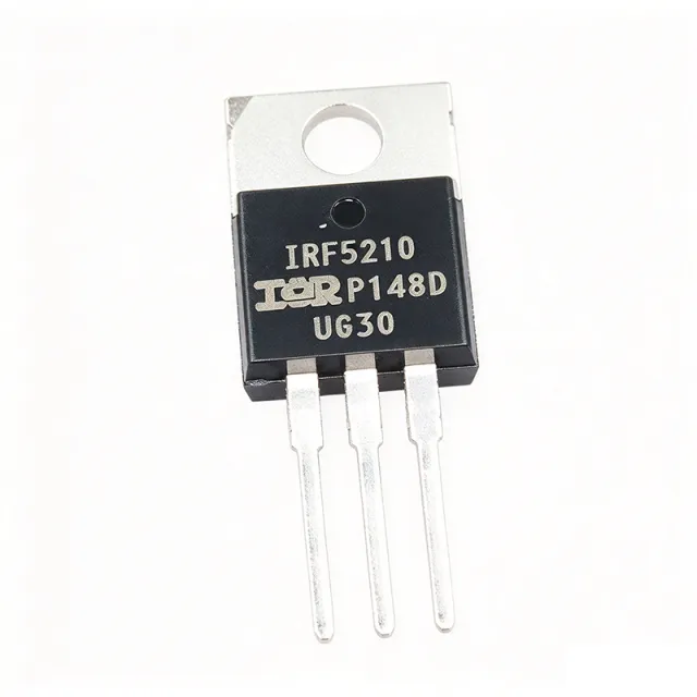
IRF5210PBF - -100V P-Channel 40A HEXFET MOSFET | Infineon
The Infineon IRF5210PBF is a P-Channel 100V HEXFET power MOSFET rated for -40A continuous drain current (Tc) and 200W power dissipation in a TO-220AB through-hole package. Originally designed by International Rectifier and now produced by Infineon after the 2015 acquisition, this Fifth Generation HEXFET device uses advanced processing to achieve extremely low on-resistance per silicon area, with a typical Rds(on) of 60 milliohms at Vgs = -10V. A P-Channel MOSFET is a type of field-effect transistor where the channel conductivity is induced by a negative gate-to-source voltage. P-Channel devices are used as high-side switches because their source is connected near the load supply rail and turning the device on only requires pulling the gate below the source by Vgs(th), which simplifies gate drive in many 24V and 48V systems. The IRF5210PBF fits into the broader taxonomy of MOSFET -> power MOSFET -> discrete semiconductor, making it a fundamental building block of power electronics. Key features include a drain-to-source voltage rating of -100V, continuous drain current of -40A at Tc, avalanche-rated ruggedness for unclamped inductive switching, and a low typical on-resistance of 60 milliohms. The TO-220AB package provides a thermal resistance of around 0.75 C/W junction-to-case, enabling reliable operation at high power levels. The PBF suffix confirms lead-free, RoHS-compliant construction suitable for global commercial and industrial designs. Technically, the device uses Infineon's fifth-generation HEXFET process technology with a vertical DMOS structure, optimized for low conduction loss and fast switching. The typical total gate charge of 120 nC allows moderate-frequency PWM operation. The intrinsic body diode supports synchronous-rectifier-style applications and free-wheeling current paths. Typical applications include high-side load switches, DC motor control, solenoid drivers, power OR-ing, hot-swap controllers, and uninterruptible power supplies. It is widely deployed in industrial 24V/48V bus systems where P-Channel high-side switching simplifies gate drive architecture. When designing with this part, ensure the gate drive pulls at least 10V below the source for full enhancement, and verify SOA at peak load conditions. The TO-220AB tab is electrically tied to the drain; insulator kits are required when mounting to a grounded heatsink. This page synthesizes distributor pricing, drop-in same-package alternatives, and practical high-side-switching design notes not found in the manufacturer datasheet.

IRF5305PBF - 55V P-Ch HEXFET MOSFET 31A TO-220 | Infineon
The Infineon IRF5305PBF is a P-Channel HEXFET power MOSFET rated at -55V VDS, -31A continuous drain current (Tc), and 110W maximum power dissipation, housed in a TO-220AB through-hole package. Built on Infineon's fifth-generation HEXFET process, it delivers a typical on-resistance of 60 mOhm at VGS = -10V and a total gate charge of 42 nC, making it well suited for high-efficiency switching conversion and low-side motor control. A P-Channel MOSFET is a type of metal-oxide-semiconductor field-effect transistor in which the channel conducts when the gate is pulled below the source potential. P-Channel devices sit at the top of a high-side switch (source at the load supply, drain at the load) and simplify gate-drive circuitry when the system logic ground equals the load ground. Within the broader semiconductor taxonomy, the IRF5305PBF belongs to: power MOSFET -> discrete semiconductor -> power management semiconductor. As a 'P-Channel complement' to the popular N-Channel IRF540N, it enables push-pull half-bridge and synchronous-rectifier topologies using a single ground-referenced gate drive. Key features include a low typical RDS(on) of 60 mOhm at VGS = -10V, avalanche-rated energy (EAS) per the HEXFET ruggedness spec, fast switching thanks to low Qg and Qgd, and an industry-standard TO-220AB outline with the gate, drain, and source pins on the tab, tab, and 3-pin row respectively. The 'PBF' suffix confirms lead-free (Pb-free) terminal plating compliant with RoHS. Architecturally, the IRF5305PBF uses Infineon's planar HEXFET cell structure with a vertical DMOS die, allowing high current density and avalanche capability. The through-hole TO-220AB tab provides a low thermal resistance path (~1.0 C/W junction-to-case) so the device can dissipate 110W at TC = 25C with appropriate heatsinking. Typical applications include high-side switching in 12V/24V automotive and industrial systems, DC motor direction control (H-bridge), load switching and OR-ing, power OR-ing for redundant supplies, and buck/boost converters where a P-Channel high-side switch is preferred for simplicity. The -55V rating gives wide margin for 24V and 40V industrial buses. When designing with the IRF5305PBF, ensure the gate is pulled fully to at least -10V relative to the source to achieve the rated on-resistance; a logic-level MOSFET is preferable if the driver swings only to -5V. Always heatsink the tab for continuous currents above a few amperes and respect the SOA at high VDS. This page synthesizes distributor pricing, drop-in alternatives, and practical design notes not found in the manufacturer datasheet alone.
IRF5305STRLPBF - 55V P-Ch MOSFET 31A 60mΩ | Infineon
The Infineon IRF5305STRLPBF is a P-channel HEXFET power MOSFET rated at -55V VDS, -31A continuous drain current (at TC), and 60 mOhm maximum on-resistance at VGS = -10V, supplied in a surface-mount D2PAK (TO-263) package and shipped on tape-and-reel (TR) packaging with lead-free (Pb-free) plating. This fifth-generation HEXFET device leverages advanced process technology to achieve extremely low on-resistance per silicon area while maintaining fast switching speed and rugged avalanche-rated performance. A P-channel power MOSFET is a voltage-controlled majority-carrier device in which the channel is formed by holes; this polarity allows it to be used as a high-side switch with a simple gate-drive referenced to ground, which simplifies driving circuits in low-voltage battery and USB power-path applications. Within the broader taxonomy, the IRF5305 belongs to the discrete-semiconductor MOSFET family, which itself sits under power transistors and ultimately under the wider power-management electronics hierarchy. Key features include 60 mOhm R_DS(on) max at VGS = -10V, 110 W maximum power dissipation at TC, a logic-level compatible threshold that achieves low R_DS(on) at VGS = -4.5V, and a continuous drain current of -31A. The device is avalanche-rated, lead-free (Pb-free), RoHS-compliant, and supplied on 800-piece tape-and-reel. The D2PAK package provides a low thermal resistance path through the PCB drain pad, enabling high-current operation with a minimal heatsink or copper pour. The IRF5305 uses Infineon's fifth-generation HEXFET stripe-cell planar technology, which minimizes JFET and accumulation resistance contributions to R_DS(on). The body diode exhibits a soft reverse-recovery characteristic that reduces switching losses and EMI in half-bridge and synchronous-rectifier topologies, while the ruggedized die design supports unclamped inductive switching (UIS) for motor-drive and solenoid applications. Typical applications include battery protection and power-path management in portable and battery-powered systems, high-side load switching for motors and solenoids, DC-DC converter high-side switches, reverse-polarity protection circuits, and power-ORing for redundant supplies. The wide -55V rating also suits 24V industrial bus switching with substantial transient margin. When designing with this device, pay attention to gate-drive voltage headroom: although R_DS(on) is specified at VGS = -10V, the device is characterized for low-side-of-spec R_DS(on) at VGS = -4.5V, allowing direct 5V microcontroller drive. Always derate continuous drain current with mounting pad area and ambient temperature using the SOA curves in the datasheet. This page synthesizes distributor pricing, parametric comparison, and drop-in D2PAK alternatives not consolidated on the manufacturer datasheet alone.
IRF5305STRRPBF - P-CH 55V 31A HEXFET MOSFET D2PAK | Infineon
The Infineon IRF5305STRRPBF is a P-channel power MOSFET built on the company's HEXFET advanced-process technology, rated for -55 V VDS and continuous drain current up to 31 A at TC, delivered in a surface-mount D2PAK (TO-263) package. The device achieves a maximum on-resistance of 60 mOhm at VGS = -10 V and dissipates up to 110 W at TC. It is offered as a RoHS-compliant, lead-free part (Pb-free suffix) and ships in tape-and-reel packaging for high-volume assembly. A power MOSFET (metal-oxide-semiconductor field-effect transistor) is a voltage-controlled switch used to deliver large currents efficiently in DC-DC conversion, motor drive, and load-switching circuits. Within the power-management hierarchy, it sits below the IC-level controller and above the discrete wiring layer, providing the high-current, low-loss switching element. P-channel MOSFETs are particularly common in high-side switching because they can be driven from a low-side gate signal without a charge pump, simplifying gate-drive architecture. Key differentiating features include an avalanche-rated body diode, dynamic dv/dt ruggedness, and a logic-compatible -10 V gate-drive threshold that pairs cleanly with industry-standard gate drivers. The D2PAK footprint supports substantial PCB copper heatsinking, allowing continuous operation near the 31 A TC rating with proper thermal design. Low thermal resistance and a wide operating junction temperature range of -55C to +175C enable deployment in harsh automotive under-hood, industrial, and power-tool environments. The IRF5305STRRPBF uses HEXFET cell technology that minimizes RDS(on) per unit silicon area, balancing conduction loss with switching speed for sub-100 kHz applications. Its P-channel polarity makes it ideal for reverse-battery protection, high-side load switches, and synchronous rectifier low-side replacements in buck converters where N-channel drive complications are undesirable. Typical applications include DC motor speed control, solenoid drivers, high-side load switching in 12 V/24 V automotive systems, uninterruptible power supply (UPS) battery switching, and synchronous rectification in buck converters. The device is also used in power OR-ing for redundant supplies and in audio amplifier output stages. When designing with the IRF5305STRRPBF, ensure the gate-drive circuit can pull VGS to -10 V for full enhancement and that PCB copper area is sized for the expected continuous dissipation. P-channel devices conduct when the gate is pulled below the source, so gate-drive timing must be coordinated with downstream logic-level signals. Use a gate-source resistor to prevent unintended turn-on during transients. This page synthesizes distributor pricing, verified drop-in alternatives, application notes, and D2PAK thermal design guidance not consolidated in any single manufacturer document, providing engineering value beyond the original IRF5305 datasheet.
IRF530NPBF - 100V N-Channel HEXFET MOSFET 17A TO-220 | Infineon
The Infineon IRF530NPBF is an N-channel HEXFET power MOSFET rated for 100 V VDS and 17 A continuous drain current (at Tc) in a TO-220AB through-hole package. It uses advanced process technology to deliver extremely low on-resistance per silicon area, combined with fast switching speed and ruggedized avalanche-rated construction, giving designers an efficient and reliable switch for a wide variety of power-conversion and motor-drive topologies. A power MOSFET is a voltage-controlled semiconductor switch in which the gate field modulates a conduction channel between source and drain. The HEXFET family pioneered by International Rectifier (now part of Infineon) uses a hex-cell layout that maximizes channel width per unit area, lowering RDS(on) and conduction losses. Within the broader taxonomy, IRF530NPBF sits as: power MOSFET -> N-channel enhancement-mode MOSFET -> discrete semiconductor -> semiconductor device. Its standard TO-220 footprint and gate-threshold range make it directly compatible with thousands of legacy designs from the early 1990s onward. Key specifications include a maximum drain-source voltage of 100 V, continuous drain current of 17 A at Tc, pulsed current capability above 50 A, and static drain-source on-resistance in the tens of milliohms range that drops with higher VGS. The device is fully avalanche rated, has a dv/dt ruggedness rating, and operates from -55 C to +175 C junction temperature. The TO-220AB package provides a low thermal-resistance path that can dissipate approximately 70 W at Tc. The IRF530NPBF uses Infineon's advanced planar cell process, which combines a vertical DMOS structure with optimized cell pitch to minimize specific on-resistance. This yields a low figure-of-merit (RDS(on) x Qg) compared with older-generation devices, reducing both conduction and switching losses. The die is avalanche-rated, meaning it can absorb the energy stored in stray inductance during turn-off without degradation, which is essential for inductive loads such as motors and solenoids. Typical applications include DC motor drives and H-bridges, solenoid and relay drivers, switching-mode power supplies (SMPS), DC-DC converters, uninterruptible power supplies (UPS), audio amplifiers, and general-purpose high-side or low-side switching in industrial and automotive subsystems. The 100 V rating comfortably supports 24 V and 48 V bus rails. When designing with this part, ensure VGS is driven above 10 V for full enhancement and minimum RDS(on). Use a gate resistor (10-100 ohm) to control ringing, and provide adequate heatsinking when continuous dissipation exceeds 2-3 W. The tab is electrically connected to the drain in TO-220. This page synthesizes distributor pricing, drop-in TO-220 alternatives, and practical design notes not found in the manufacturer datasheet.

IRF530NSTRLPBF - 100V 17A N-Channel HEXFET MOSFET | Infineon
The Infineon IRF530NSTRLPBF is an N-channel 100V 17A HEXFET power MOSFET in a surface-mount D2PAK (TO-263) package delivering 90 mOhm max on-resistance at 10V VGS and 70W continuous power dissipation at Tc=25C. The device belongs to Infineon's HEXFET Power MOSFET family and uses advanced processing techniques to achieve extremely low on-resistance per silicon area, combined with fast switching speed and ruggedized device design. A power MOSFET (Metal-Oxide-Semiconductor Field-Effect Transistor) is a voltage-controlled semiconductor switch used to switch and amplify signals in power electronics. Power MOSFETs sit within the discrete semiconductor hierarchy as transistors -> MOSFETs -> power MOSFETs, serving as the workhorse switching element in switched-mode power supplies, motor drivers, and load switching circuits. The N-channel enhancement-mode configuration of the IRF530NSTRLPBF means current flows from drain to source when a positive gate-source voltage exceeds the threshold. Key specifications include 100V drain-to-source breakdown voltage (V(BR)DSS), 17A continuous drain current at Tc=25C, 90 mOhm max static drain-source on-resistance at VGS=10V, and 24.7 nC total gate charge. The D2PAK surface-mount package features a low thermal resistance path through the drain tab to the PCB copper pad, enabling 70W dissipation at case temperatures below 25C with proper PCB thermal design. The IRF530NSTRLPBF utilizes Infineon's proprietary HEXFET stripe-cell planar technology, which optimizes cell density to balance on-resistance, switching loss, and avalanche ruggedness. The fast switching speed supports PWM frequencies above 100 kHz in DC-DC converter and motor-drive applications, while the avalanche-rated design provides robustness against inductive switching transients. Typical applications include switched-mode power supplies (SMPS), DC motor speed controls, uninterruptible power supplies (UPS), solenoid drivers, and high-side/low-side switching in power conversion stages. The 100V rating provides ample headroom for 48V telecom bus, 24V industrial, and 12V automotive subsystems. When designing with this device, ensure the gate drive voltage reaches at least 10V to achieve the specified 90 mOhm RDS(on). The D2PAK package requires substantial PCB copper area (typically 1 sq inch minimum) to achieve rated power dissipation, otherwise de-rate aggressively with thermal calculations. This page synthesizes distributor pricing, drop-in alternative cross-references, and practical thermal design notes not consolidated in the manufacturer datasheet alone, giving engineers actionable intelligence for sourcing and design-in decisions.

IRF540 - 100V 22A N-Channel Power MOSFET | STMicroelectronics
The STMicroelectronics IRF540 is an N-channel power MOSFET rated 100 V drain-source voltage (VDSS), 22 A continuous drain current at Tc, and 85 W power dissipation at Tc, housed in a through-hole TO-220 package. It uses ST's avalanche-rugged technology with typical RDS(on) of 0.050 ohm and 100% avalanche testing at production. A power MOSFET is a voltage-controlled semiconductor switch that forms the top layer of the power semiconductor hierarchy: transistor -> MOSFET -> power MOSFET -> power management. Unlike bipolar junction transistors, MOSFETs are driven by gate voltage rather than base current, giving very high input impedance, fast switching, and low drive power. This makes them the default choice for switching converters, motor drives, and load switches in modern power electronics. Key features of the IRF540 include its 100 V avalanche-rugged drain-source rating, repetitive avalanche data specified at 100 C, low total gate charge for efficient gate driving, high current capability up to 22 A (case temperature), and a 175 C maximum operating junction temperature. The 100% avalanche test in production guarantees uniform ruggedness against inductive kickback events, an important reliability differentiator versus non-avalanche-rated devices. Architecturally, the IRF540 family is based on a vertical power MOSFET structure optimized for the classic industry-standard IRF pinout: gate, drain, source on the TO-220 tab package. The typical 0.050 ohm on-resistance limits conduction loss to roughly 12 W at a 22 A continuous load (estimated: I^2 x R = 22 A squared x 0.050 ohm), while the low gate charge reduces switching losses in PWM converters operating at tens to hundreds of kilohertz. Typical applications include DC-DC converter switching stages, DC motor speed control and H-bridges, inverter and UPS output stages, and general-purpose high-current load switches. The 100 V rating comfortably covers 12 V, 24 V, and 48 V industrial buses with ample transient headroom, which is why the IRF540 remains a workhorse in both hobbyist and industrial designs. Design-wise, drive the gate with at least 10 V for full enhancement and lowest RDS(on); logic-level drive at 5 V will substantially increase on-resistance. Always verify thermal margins with proper heatsinking, since the TO-220 package requires an effective thermal path at multi-watt dissipation. This page synthesizes cross-manufacturer drop-in alternatives, parametric comparison data, and practical design notes beyond what a single datasheet provides, saving engineers cross-referencing time.

IRF540NSTRLPBF - 100V 33A N-Channel MOSFET D2PAK | Infineon
The Infineon IRF540NSTRLPBF is a 100 V, 33 A N-channel HEXFET power MOSFET housed in a surface-mount D2PAK (TO-263) package, supplied on a 13-inch reel. It uses Infineon's advanced process technology to deliver a maximum on-resistance of 44 mOhm at VGS = 10 V and a typical gate charge of 47.3 nC, giving an excellent figure of merit (FOM) for hard-switched power-conversion stages. An N-channel power MOSFET is a voltage-controlled majority-carrier device whose drain current is modulated by the gate-to-source voltage. Within the broader taxonomy, N-channel MOSFETs sit below power MOSFETs, which in turn belong to the discrete semiconductor family of transistors. They are typically preferred over P-channel devices in low-side switching or synchronous-rectifier positions because their lower Rds(on) per unit silicon area reduces conduction loss. Key features of the IRF540NSTRLPBF include a continuous drain current of 33 A at Tc = 25 C, a pulsed drain current rating suitable for inductive loads, and a power dissipation of 130 W at Tc = 25 C. The D2PAK surface-mount footprint allows direct attachment to a PCB copper pour that serves as both electrical ground and thermal heatsink, simplifying mechanical assembly compared to the through-hole TO-220 variant of the same die. The device uses Infineon's HEXFET stripe-cell planar structure with a vertical DMOS architecture, optimized for low on-resistance per die area. The avalanche-rated body diode and high dv/dt immunity make the part robust against the voltage transients seen in motor and solenoid switching. Thermal resistance junction-to-case is on the order of 1.0 C/W, enabling the 130 W dissipation figure when the case is properly soldered to a sufficient copper area. Typical applications include DC motor drives in industrial automation, solenoid and relay drivers, low-frequency switching regulators, LED drivers, battery protection circuits, and uninterruptible power supplies. The 100 V Vds rating gives comfortable margin on 24 V and 48 V buses. When designing with this part, ensure that the PCB copper area under the D2PAK tab is sized to keep the junction below 150 C at worst-case load. A 10 V gate drive is required for full enhancement; logic-level (5 V) microcontrollers must use a gate-driver stage. This page synthesizes distributor pricing, drop-in same-package alternatives, and practical thermal and gate-drive design notes not found in the manufacturer datasheet.
IRF540ZPBF - 100V 36A N-Channel HEXFET MOSFET | Infineon
The Infineon IRF540ZPBF is a 100 V, 36 A N-channel HEXFET Power MOSFET in a TO-220AB through-hole package, designed using advanced process technology to deliver extremely low on-resistance per silicon area. It features 26.5 mOhm maximum R_DS(on) at V_GS=10V, 42 nC total gate charge, 175 degC maximum junction temperature, and improved repetitive avalanche ruggedness. These characteristics make it an extremely efficient and reliable device for automotive-grade power switching applications. A power MOSFET (Metal-Oxide-Semiconductor Field-Effect Transistor) is a voltage-controlled switch used to efficiently switch and amplify signals in power electronics. The HEXFET family represents Infineon's optimized vertical DMOS architecture, which falls under the broader categories of: discrete semiconductor -> MOSFET -> N-channel MOSFET -> power MOSFET -> switching transistor. The IRF540Z series specifically targets the 100 V breakdown class, occupying a middle position between low-voltage logic-level parts and high-voltage IGBTs, and is widely used for synchronous rectification, DC-DC conversion, motor drive, and relay replacement. Key features of the IRF540ZPBF include ultra-low on-resistance (26.5 mOhm max), fast switching speed enabled by low Q_g (42 nC typical), fully avalanche-rated design, and a TO-220AB package with industry-standard pinout that allows direct drop-in replacement of legacy IRF540-series parts. The device is also qualified for automotive environments, with extended temperature range and enhanced reliability testing. Technically, the IRF540ZPBF uses a stripe-cell DMOS design with a polysilicon gate, achieving an excellent figure-of-merit (FOM = R_DS(on) x Q_g) for its voltage class. The 175 degC maximum junction temperature and 92 W power dissipation rating give designers substantial thermal headroom in industrial and automotive systems. Compared with older IRF540 generations, the 'Z' suffix variant offers significantly lower on-resistance while preserving the same TO-220AB footprint. Typical applications include DC motor drives in automotive and industrial systems, solenoid and relay drivers, switching-mode power supplies (SMPS) primary-side switches, DC-DC converters, battery protection circuits, and general-purpose high-current switching. It is widely used as an upgrade for IRF540N, IRF640, and similar 100 V-class MOSFETs. When designing with the IRF540ZPBF, ensure the gate driver can source and sink sufficient peak current (typically 1-2 A) to charge the input capacitance within the desired switching interval. A 10 Ohm gate resistor is recommended to damp ringing, and the drain-source avalanche energy must be derated according to junction temperature using the SOA curves in the datasheet. This page synthesizes distributor pricing, parametric drop-in alternatives, and practical design notes beyond what the manufacturer datasheet alone provides, enabling faster BOM decisions and second-source qualification.
IRF5N5210 - -100V P-CH HEXFET MOSFET, SMD-1 | International Rectifier
The International Rectifier IRF5N5210 is a -100V, -31A P-channel HEXFET power MOSFET in a surface-mount SMD-1 package, qualified to MIL-PRF-19500 for high-reliability applications. It is a Fifth-Generation HEXFET device from International Rectifier (now Infineon Technologies), using advanced processing techniques to achieve the lowest possible on-resistance per silicon unit area. The datasheet reference number is PD-94154B and it carries Hi-Rel validation per the manufacturer. A P-channel MOSFET (PMOS) is a type of field-effect transistor in which the majority carriers are holes; it is turned ON by pulling the gate voltage below the source voltage. PMOS devices sit at the high-side of a load in many switching topologies and simplify low-side drive designs because the gate can be referenced to ground. Within the power-MOSFET taxonomy, the IRF5N5210 belongs to the HEXFET family of planar/HEX-cell MOSFETs, the broader discrete-semiconductor hierarchy, and is qualified for high-energy pulse and aerospace/defense circuits. This P-channel construction simplifies gate drive in high-side switching because no charge pump is required. Key electrical specifications include a -100V drain-source breakdown (V(BR)DSS), -31A continuous drain current (ID), and HEXFET cell architecture that minimizes RDS(on) per unit area. The device features high transconductance, superior avalanche energy rating, and reverse-recovery dv/dt capability, enabling robust operation in inductive-switching environments. The SMD-1 surface-mount package provides a low-profile footprint suitable for high-density PCBs while maintaining the high-current handling required for power applications. Typical applications include power supplies (as a high-side switch), motor control circuits, chopper circuits, audio amplifiers, and other high-energy pulse applications. The MIL-PRF-19500 qualification makes it particularly suitable for military, aerospace, and other high-reliability environments where ruggedness and proven performance are required. When designing with the IRF5N5210, note that P-channel MOSFETs require the gate voltage to be pulled below the source to turn on, which usually means the gate driver must be referenced to the source node. For switching applications, ensure proper gate-source resistance to control switching speed and prevent false triggering from dv/dt transients. The high avalanche rating allows unclamped inductive switching within the published energy limits. This page synthesizes manufacturer datasheet values, MIL-PRF-19500 qualification status, parametric drop-in alternatives, and high-reliability design guidance that is not duplicated on distributor listing pages.
IRF640NPBF - 200V 18A N-Channel HEXFET MOSFET TO-220 | Infineon
The Infineon IRF640NPBF is a fifth-generation HEXFET N-channel power MOSFET rated at 200 V VDS, 18 A continuous drain current at Tc, and 150 W power dissipation, housed in a TO-220AB through-hole package. It features a maximum on-resistance of 150 mOhm at VGS = 10 V and a total gate charge of 44.7 nC, making it a workhorse part for medium-voltage switching applications. A power MOSFET is a voltage-controlled semiconductor switch that uses an insulated gate (typically silicon dioxide) to modulate current flow between the source and drain terminals. HEXFET is Infineon's trade name (originally International Rectifier's) for its vertical-cell, hex-shaped power MOSFET structure that maximises channel density per silicon area and minimises on-resistance. Within the broader hierarchy, the IRF640NPBF sits under: power MOSFET -> discrete power transistor -> discrete semiconductor -> electronic component. Key features include extremely low on-resistance per silicon area (a fifth-generation HEXFET hallmark), fast switching speed, dynamic dv/dt rating, full avalanche ruggedness, and a maximum operating junction temperature of 150 C. The TO-220AB package with its mounting tab enables direct heatsink attachment, and the simple three-terminal gate-source-drain configuration allows direct drive from standard 10 V logic-level gate drivers without intermediate buffer stages. The fifth-generation HEXFET cell geometry combines advanced process techniques with a stripe-cell layout to deliver low RDS(on) per unit area while preserving the ruggedness and avalanche-energy rating that earlier generations were known for. Internally, the gate structure is optimised for fast switching and high dv/dt immunity, important in off-line SMPS, motor drive, and inverter applications where ringing and transient stresses can destroy lesser parts. The TO-220AB package also provides generous creepage distance well-suited to 200 V rails. Typical applications include switched-mode power supplies (SMPS), DC-DC converters, motor drivers, relay and solenoid replacement circuits, battery management, uninterruptible power supplies (UPS), and low-frequency (<100 kHz) inverters for audio amplifiers, lighting ballasts, and induction heating. The 200 V rating gives comfortable headroom for rectified 120 V mains or 48 V telecom rails with margin for inductive spikes. When designing with this part, ensure gate-drive headroom is correct (VGS = 10 V is recommended for lowest RDS(on)), add a gate-source resistor (typically 10-100 ohm) to suppress parasitic oscillation, and verify that the heatsink keeps Tj below 150 C under worst-case SOA conditions. The TO-220AB tab is electrically connected to the drain, so isolate with a thermal pad (e.g. silicone rubber with mica or ceramic) if the heatsink is grounded. This page synthesises distributor pricing, drop-in TO-220AB alternatives, and practical thermal and PCB design notes not found in the bare manufacturer datasheet, giving engineers a single reference for sourcing and designing with the IRF640NPBF.
IRF640NSTRLPBF - 200V 18A N-Channel HEXFET MOSFET | Infineon
The Infineon IRF640NSTRLPBF is a fifth-generation HEXFET N-channel power MOSFET rated at 200V VDS, 18A continuous drain current (Tc), and 150W maximum power dissipation, housed in a surface-mount D2PAK (TO-263AB) package with a tape-and-reel suffix. It features a typical on-resistance of 0.15 ohm at VGS=10V and a total gate charge of 44.7 nC, providing an optimized balance between conduction losses and switching speed for high-voltage power conversion. A power MOSFET (Metal-Oxide-Semiconductor Field-Effect Transistor) is a voltage-controlled three-terminal semiconductor switch that uses an insulated gate to modulate conduction between the drain and source terminals. N-channel MOSFETs like the IRF640NSTRLPBF are the workhorses of switched-mode power supplies (SMPS), motor drives, and DC-DC converters. The HEXFET (HEXagonal cell) topology pioneered by International Rectifier (now Infineon) places many parallel hexagonal cells across the die to minimize RDS(on) per unit silicon area, dramatically lowering conduction losses compared to planar stripe designs. N-channel devices occupy the upper position of the power-MOSFET hierarchy: N-channel MOSFET -> power MOSFET -> discrete semiconductor -> power management component. Key features include an ultra-low on-resistance of 0.15 ohm, fast switching with low gate charge of 44.7 nC, avalanche-rated ruggedness, and a logic-level-compatible VGS(th) range. The D2PAK package exposes the metal tab for low-thermal-resistance PCB mounting, achieving much higher continuous current than a comparably rated TO-220 part on equivalent copper area. This device is also lead-free (PbF suffix) and RoHS-compliant. The IRF640NSTRLPBF is built on Infineon's advanced process technology that combines trench-gate structures with optimized cell density, achieving the lowest possible RDS(on) × Qg figure of merit. This translates directly to lower switching and conduction losses in high-frequency applications, and the ruggedized device design supports unclamped inductive switching events common in motor and solenoid drive circuits. Typical applications include switched-mode power supplies (SMPS), DC motor speed controls, uninterruptible power supplies (UPS), and high-voltage buck/boost converters. The 200V rating makes it especially well suited for 120V/170V offline rectified bus rails and 48V telecom secondary-side switching. When designing with this part, gate-drive voltage of 10V VGS is required to fully enhance the channel and achieve the datasheet 0.15 ohm RDS(on); a 10 ohm gate resistor dampens ringing. The exposed metal tab should be soldered to a copper pour of at least 1 square inch for full 150W rated performance. This page synthesizes distributor pricing, drop-in HEXFET alternatives from the same family, and practical thermal/layout design notes not found in the manufacturer datasheet alone.

IRF7103TRPBF - 50V Dual N-Channel MOSFET, 3A, SO-8 | Infineon
The Infineon IRF7103TRPBF is a dual N-channel power MOSFET in a surface-mount SO-8 package, rated for 50V VDS, 3A continuous drain current, and 130 mOhm maximum on-resistance. It uses Infineon's advanced IR MOSFET™ process technology and is qualified to industrial standards for low- to medium-power switching applications. An N-channel power MOSFET is a voltage-controlled semiconductor switch that conducts current when a gate-source voltage exceeds the threshold. Dual MOSFET arrays integrate two independent MOSFETs in one package to save PCB area in half-bridge, synchronous-rectification, and load-switch topologies. The IRF7103 belongs to the power-MOSFET -> discrete semiconductor -> active component hierarchy. Key features include a low on-resistance of 0.11 ohm (typ.) at VGS=10V, a logic-level capable gate threshold, and fast switching speeds optimized for DC-DC conversion. The SO-8 (PG-DSO-8-902) package has been modified with a customized leadframe for enhanced thermal characteristics and dual-die capability, allowing up to 2W power dissipation per the manufacturer datasheet. The trench-based IR MOSFET™ cell structure minimizes conduction losses while maintaining robust avalanche ruggedness. Typical applications include synchronous rectification in buck converters, half-bridge motor drive, low-side load switching in industrial controls, battery protection circuits, and DC fan drivers. The dual-die common-source configuration makes it ideal for synchronous step-down (buck) topologies where two low-side switches are needed. When designing with this part, ensure the gate drive voltage reaches at least 10V for full enhancement and lowest RDS(on). Add a gate-source resistor (typ. 10 kOhm) to prevent unintended turn-on from dv/dt-induced Miller coupling, and observe the SOA envelope for pulsed loads above 3A. The thermal pad should be soldered to a sufficient copper pour for rated 2W dissipation. This page synthesizes distributor pricing, drop-in SO-8 alternatives, parametric data, and practical PCB layout guidance that goes beyond the manufacturer datasheet alone.