MOSFETs
Produits (1294)

IQEH46NE2LM7UCGSCATMA1 - 25V 440A OptiMOS 7 N-FET | Infineon
The Infineon IQEH46NE2LM7UCGSCATMA1 is an N-channel OptiMOS 7 power MOSFET rated for 25 V VDS, delivering 440 A continuous ID (at TC) in a compact 3.3x3.3 mm Source-Down PQFN (PG-WHTFN-9-1) package. It achieves an ultra-low maximum on-resistance of 0.46 mOhm and supports up to 57 A continuous drain current at TA (25 C ambient), making it ideal for high-current switching in tightly constrained PCB footprints. An N-channel power MOSFET (Metal-Oxide-Semiconductor Field-Effect Transistor) is a voltage-controlled three-terminal switch used to efficiently route and switch high currents in power conversion systems. Belonging to the MOSFET -> power MOSFET -> discrete semiconductor hierarchy, OptiMOS 7 represents Infineon's latest generation of low-voltage (typically <60 V) trench MOSFETs optimized for both hard- and soft-switching topologies including buck, buck-boost, and totem-pole PFC. The Source-Down packaging places the source connection on the bottom of the die, improving thermal performance and enabling top-side cooling. Key features include a 25 V drain-source breakdown rating, 0.46 mOhm max RDS(on), an operating temperature range suitable for industrial and compute applications, and an integrated source-down thermal pad. The PG-WHTFN-9-1 package provides a compact footprint optimized for high-density power designs in AI servers and data center power supplies, where every square millimeter of PCB real estate and every milliohm of conduction loss translates directly into system efficiency. From an architecture standpoint, the OptiMOS 7 process uses an advanced trench cell structure with epitaxial refinement that minimizes both on-state conduction losses (low RDS(on)) and switching losses (low Qg, low Qrr). This balance is critical for high-frequency SMPS designs where traditional MOSFETs compromise between conduction and switching performance. The Source-Down package topology further reduces package resistance and inductance by relocating the source bond wires to a direct PCB connection. Typical applications include AI server and data center 48V-to-Point-of-Load (PoL) conversion, telecom brick DC-DC converters, USB-PD and high-power USB Type-C chargers, graphics card and accelerator (GPU/ASIC) power stages, and high-frequency synchronous rectification. The low RDS(on) and small footprint make it particularly suited for AI computing platforms where multiple parallel MOSFETs are stacked to deliver hundreds of amps at low voltage. Design consideration: at 25 V VDS with potentially high di/dt transients, PCB layout must minimize source-loop inductance to control ringing and EMI. Place the gate driver within 5 mm of the gate pin and use a 1 Ohm gate-source resistor for damping. Ensure adequate copper pour on the source-down thermal pad - typically 1 oz copper minimum with thermal vias to inner planes for heat extraction. This page synthesizes Infineon OptiMOS 7 family specifications, drop-in Source-Down package alternatives, distributor stock signals, and practical design notes for AI server power applications not found in the manufacturer datasheet alone.
IQEH50NE2LM7UCGSCATMA1 - 25V OptiMOS 7 N-Ch MOSFET | Infineon
The Infineon IQEH50NE2LM7UCGSCATMA1 is an N-channel OptiMOS 7 power MOSFET rated at 25 V VDS, delivering 54 A continuous drain current at TA and 422 A at TC, with a maximum on-resistance of 0.5 mΩ, housed in a surface-mount PG-WHTFN-9-1 package. The device is engineered for peak performance in data centers, AI servers, and high-current synchronous rectification stages where ultra-low conduction loss and high power density are required. According to Infineon, the OptiMOS 7 25 V family is application-optimized for server, telecom, and AI workloads. An N-channel power MOSFET (Metal-Oxide-Semiconductor Field-Effect Transistor) is a voltage-controlled three-terminal device in which a positive gate-source voltage creates a conductive channel between drain and source. Power MOSFETs sit inside the broader semiconductor hierarchy: MOSFET -> discrete semiconductor -> power discrete -> switch-mode power conversion building block. Optimized low-voltage MOSFETs such as this part are routinely used as synchronous rectifiers on the secondary side of buck converters, where every milliohm of RDS(on) translates directly into conduction loss, efficiency, and thermal headroom. Key differentiating parameters include 25 V drain-source breakdown voltage optimized for 12 V rails, 0.5 mΩ maximum on-resistance for minimum conduction loss, 175°C rated junction temperature for harsh thermal environments, and a 2 V typical gate threshold enabling low-voltage gate drive. The device dissipates 2.5 W at TA and 150 W at TC, with PCB layout on 6 cm² of copper drain area per the datasheet characterization conditions. The PG-WHTFN-9-1 package provides top-side cooling and a small footprint suitable for high-density VRM topologies. Typical applications include AI accelerator point-of-load converters, server core voltage rails, telecom 48 V intermediate bus converters, hot-swap circuits, and OR-ing FETs in redundant power supplies. Its low RDS(on) and high current rating make it especially suitable as a synchronous rectifier where switching losses and conduction losses both matter. When designing with this part, prioritize Kelvin-source gate drive to fully realize the 0.5 mΩ rating, and use the datasheet SOA diagram to verify operation under fault and transient conditions. PCB layout should minimize source-inductance loop area and maximize copper on the drain tab for thermal spreading. This page synthesizes distributor inventory, parametric comparison with drop-in alternatives, and design notes not found in the manufacturer datasheet, helping engineers select and qualify the part faster.
IQEH50NE2LM7ZCGATMA1 - 25V 422A OptiMOS 7 N-Channel MOSFET | Infineon
The Infineon IQEH50NE2LM7ZCGATMA1 is a 25 V OptiMOS 7 N-channel power MOSFET delivering 422 A continuous drain current (Tc) and a maximum on-resistance of 0.5 mOhm in a surface-mount PG-TTFN-9-3 package. The part is specified for 25 V drain-source voltage, supports 54 A at ambient (Ta), and dissipates up to 150 W at the case (Tc) versus 2.5 W at the ambient, with a 175 degrees C maximum junction temperature rating per the Infineon datasheet. An N-channel MOSFET (Metal-Oxide-Semiconductor Field-Effect Transistor) is a voltage-controlled three-terminal switching device that conducts current between drain and source when a positive gate-source voltage exceeds the threshold. Within the broader semiconductor taxonomy, a power MOSFET belongs to the discrete power device family alongside IGBTs and thyristors, and it serves as the fundamental building block of synchronous rectification, hot-swap, and load-switch stages. The OptiMOS 7 generation from Infineon is the company's 25 V and 40 V logic-level optimized family targeting AI server, telecom, and high-density computing power rails. The IQEH50NE2LM7ZCGATMA1's headline features are its extremely low 0.5 mOhm maximum on-resistance, 422 A continuous drain current at case, and +175 degrees C operating junction temperature. These specifications enable very low conduction losses in high-current synchronous-rectifier and OR-ing applications, while the elevated temperature rating provides extra margin for hot-spot-tolerant designs. Infineon's OptiMOS 7 technology also delivers improved switching figures of merit versus prior generations, allowing higher switching frequencies with reduced gate-drive losses. Architecturally, the device uses a trench-gate silicon structure optimized for 25 V breakdown class, with the source and gate bondable from the top side and the drain exposed through the package's thermal pad. The PG-TTFN-9-3 (Infineon Thin-package Topside-Flat No-lead) footprint provides Kelvin-source connection options that minimize gate-loop inductance, an important consideration when the MOSFET is operated at high di/dt in 48 V-to-PoL conversion stages for AI processors. Typical applications include AI server 48 V intermediate bus converters, OR-ing and hot-swap controllers in redundant telecom rectifiers, synchronous-rectifier stages for telecom DC-DC bricks, e-mobility auxiliary 24 V/12 V power rails, and high-current USB-PD source switches. The combination of 25 V rating and 0.5 mOhm Rds(on) is particularly well-matched to point-of-load stages that step down 12 V or 5 V intermediate rails directly at the processor socket. When designing with this device, pay attention to PCB layout for the gate-drive loop: keep the gate-driver IC as close as possible to the gate and Kelvin-source pins to minimize parasitic inductance and ringing. Thermal management is critical at high current - use generous copper pours on the drain pad and, when possible, a multi-layer PCB with thermal vias to spread heat into inner copper planes. This page synthesizes distributor pricing, drop-in OptiMOS 7 alternatives, and practical design notes not found in the manufacturer datasheet alone.
IQEH54NE2LM7UCGATMA1 - 25V OptiMOS 7 N-Channel MOSFET | Infineon
The Infineon IQEH54NE2LM7UCGATMA1 is an OptiMOS 7 Power-Transistor N-channel MOSFET rated at 25 V VDS, with continuous drain current of 52 A (Ta) and pulsed capability up to 406 A (Tc), housed in the compact surface-mount PG-TTFN-9-3 package. It is engineered for ultra-low RDS(on) and switching loss, targeting high-frequency DC-DC conversion, OR-ing, and hot-swap applications. The device supports 2.5 W power dissipation at ambient and 150 W with case temperature control, making it suitable for thermally aggressive designs. A MOSFET (Metal-Oxide-Semiconductor Field-Effect Transistor) is a voltage-controlled semiconductor switch that conducts current between drain and source when gate-source voltage exceeds the threshold. N-channel enhancement-mode MOSFETs are the workhorse of synchronous buck converters, low-side switches, load switches, and battery protection circuits because of their low on-resistance and fast switching. The OptiMOS 7 family from Infineon is the latest 25 V-300 V generation, optimised for lowest figure-of-merit (RDS(on) x Qg) to maximise efficiency in switched-mode power supplies. Key features include 25 V drain-source voltage rating, ultra-low on-resistance, integrated gate protection, and a 9-pin TTFN package with an exposed drain pad for low thermal resistance. The part is rated for 100% UIS (avalanche) testing and is qualified to industrial-grade reliability standards, giving designers headroom for repetitive transient events on the switching node. The OptiMOS 7 technology uses Infineon's latest trench MOSFET cell architecture to push switching performance close to the theoretical silicon limit. Compared with the OptiMOS 5 generation, the FOM improvement is typically 30-50%, which directly translates to lower converter losses, smaller magnetics, and higher power density. The PG-TTFN-9-3 footprint is footprint-compatible with several Infineon OptiMOS 5/6 parts, simplifying migration. Typical applications include point-of-load (POL) regulators in servers and datacom, USB-PD power stages, synchronous buck stages in 12 V-input telecom bricks, hot-swap controllers, and battery management protection FETs. The low gate charge also makes the device attractive for high-frequency buck topologies above 1 MHz. When designing with the IQEH54NE2LM7UCGATMA1, ensure that the gate drive voltage is within the recommended 4.5 V-10 V range to achieve the datasheet RDS(on). Use a Kelvin-source connection when available to suppress source-inductance induced ringing at high di/dt, and place a 1-10 ohm gate resistor to control dv/dt-induced false turn-on in half-bridge configurations. This page synthesises distributor pricing from LCSC and DigiKey, cross-references drop-in alternatives in the same PG-TTFN-9-3 footprint, and provides design notes not found in the manufacturer datasheet.
IQEH68NE2LM7UCGATMA1 - 25V OptiMOS 7 N-MOSFET, 338A | Infineon
The Infineon IQEH68NE2LM7UCGATMA1 is an OptiMOS 7 single N-channel power MOSFET rated at 25 V drain-source breakdown, with continuous drain current of 47 A (Ta) and pulsed current capability of 338 A (Tc), housed in the surface-mount PG-TTFN-9-3 package. Per the Infineon family page, this device targets AI, server, data-center, and high-frequency hard/soft-switching applications where low conduction and switching losses are critical. The part uses Infineon's latest OptiMOS 7 silicon platform to deliver a step-change in figure-of-merit versus prior OptiMOS generations. A power MOSFET (Metal-Oxide-Semiconductor Field-Effect Transistor) is a voltage-controlled three-terminal switch used to efficiently route or modulate current in switching power supplies, motor drives, and load-management circuits. Within the broader semiconductor taxonomy, a MOSFET sits under discrete semiconductors -> transistors -> MOSFETs -> power MOSFETs -> low-voltage (<60V) synchronous rectification. OptiMOS 7 is Infineon's flagship 25V-300V platform, engineered for the highest efficiency in 12V/24V bus converters, OR-ing, and hot-swap circuits. Key features of the IQEH68NE2LM7UCGATMA1 include an industry-leading ultra-low on-resistance optimized for 10V and 4.5V gate drive (RDS(on)10 / RDS(on)45 family, per the family page snippet), a 175°C maximum operating junction temperature for harsh thermal environments, and a logic-level compatible gate threshold that simplifies microcontroller-driven designs. The TTFN-9 package exposes the drain tab for top-side or bottom-side cooling, and the small outline improves power density on the PCB. This OptiMOS 7 part is built on Infineon's advanced trench MOSFET process with an optimized cell pitch and shield-gate geometry, which lowers gate charge (Qg) and output capacitance (Coss) to minimize switching loss at high frequencies. The result is a robust 25V device suitable for continuous hard-switching operation at 500 kHz+ while keeping thermals within an FR4 PCB footprint of roughly 6 cm² copper per the datasheet's derating guidance. Typical applications include AI-server 12V intermediate bus converters, point-of-load (POL) synchronous rectification stages, hot-swap / OR-ing controllers in 24V telecom and data-center backplanes, USB-PD and high-current laptop charging, and high-frequency motor drive half-bridges. The 175°C rating also suits automotive 12V/24V load-dump-tolerant subsystems and industrial eFuse stages. When designing with this part, observe the datasheet's thermal derating on a 40 mm x 40 mm x 1.5 mm FR4 PCB with 6 cm² copper, and maintain VGS within the datasheet-specified maximum. Use a gate-driver capable of sub-50ns rise/fall times to fully exploit the low Qg, and place the gate-source resistor close to the IC pins to prevent parasitic turn-on. This page synthesizes real-time distributor pricing, drop-in same-package alternatives, and application-specific design guidance not found in the manufacturer datasheet alone.
IQEH84NE2LM7UCGATMA1 - 25V OptiMOS 7 N-FET, 275A | Infineon
The Infineon IQEH84NE2LM7UCGATMA1 is an N-channel 25 V OptiMOS™ 7 power MOSFET rated for 42 A continuous drain current at Ta (ambient, surface-mount) and 275 A pulsed drain current at Tc, with a power dissipation of 2.5 W at Ta and 107 W at Tc, housed in the surface-mount PG-TTFN-9-3 package. As an OptiMOS 7 25 V generation device, it is positioned for both hard- and soft-switching topologies, where RDS(on) of 1.0 mΩ (typ @10 V) and 4.5 mΩ (typ @4.5 V) deliver conduction-loss reduction versus prior OptiMOS generations. A MOSFET (Metal-Oxide-Semiconductor Field-Effect Transistor) is a voltage-controlled semiconductor switch used for power conversion, motor drive, and load switching. It belongs to the hierarchy: discrete semiconductor → transistor → FET → power MOSFET. The 25 V OptiMOS 7 family sits at the low-voltage end of Infineon's power MOSFET portfolio, optimised for synchronous rectification, OR-ing, hot-swap, and battery-protection switching in telecom, server, and e-mobility auxiliary systems. Key differentiators include an ultra-low RDS(on) of 1.0 mΩ typical at VGS=10 V, gate-charge optimisation for fast turn-on/off transitions, a 175 °C operating junction temperature rating, and an exposed-die/source-down PG-TTFN-9-3 package engineered for minimal thermal resistance from junction to PCB. The OptiMOS 7 cell architecture trims both switching and conduction losses versus OptiMOS 5/6 predecessors, allowing higher current density per footprint. The PG-TTFN-9-3 package provides a top-side-cooled source-down land pattern that pulls heat directly into the PCB copper, eliminating top-side heatsinking. The 175 °C Tj-max rating supports operation in confined, high-ambient environments such as server SMPS secondary-side synchronous rectification stages and 12 V/24 V hot-swap controllers. The VGS(th) is characterised in the low-voltage logic-level range, simplifying gate drive from 5 V-class MCUs or PWM controllers. Typical applications include synchronous rectification in 12 V-25 V DC-DC buck converters, hot-swap / eFuse protection in server 12 V rails, battery protection and load switching in 24 V battery packs, OR-ing FETs in redundant telecom supplies, and motor drive half-bridges in low-voltage BLDC fans and pumps. For all applications, the source-down PG-TTFN-9-3 footprint lets PCB copper serve as the heatsink. When designing with this part, observe the SOA curve carefully: although it can pulse 275 A, sustained DC current at Ta is limited by 2.5 W dissipation. Maximise copper area on source pads to keep Tj below 125 °C; derate above 80 °C ambient for reliability. Pair it with a gate-driver capable of >2 A peak source/sink current to exploit OptiMOS 7's low Qg and fast switching edges. This page synthesises Infineon OptiMOS 7 family datasheet parameters, Infineon part-page electrical ratings, distributor pricing as of 2026-09-15, and a drop-in alternative list drawn from same-family Infineon parts, not found on the bare distributor listings.
IQFH55N04NM6ATMA1 - 40V 451A 0.55mΩ OptiMOS 6 MOSFET | Infineon
The Infineon IQFH55N04NM6ATMA1 is an N-channel normal-level power MOSFET built on Infineon's latest OptiMOS 6 process technology, rated at 40 V drain-source breakdown and offering an ultra-low typical R_DS(on) of 0.55 mΩ. The device delivers continuous drain current up to 53 A at TA=25°C and a pulsed case-rated current up to 451 A (TC), housed in the compact clip-based PQFN 8x6 mm² package (PG-TSON-12-1). A power MOSFET (Metal-Oxide-Semiconductor Field-Effect Transistor) is a voltage-controlled switching device used as the core building block of power management circuits. Within the broader taxonomy, this part belongs to: discrete semiconductor -> transistor -> MOSFET -> N-channel enhancement-mode power MOSFET -> low-voltage (<=100 V) power MOSFET -> synchronous rectifier / load switch. The IQFH55N04NM6ATMA1 belongs to Infineon's OptiMOS 6 family, which represents the 6th generation of Infineon's optimized trench MOSFET platform aimed at minimizing conduction and switching losses simultaneously. Key features include a maximum static drain-source on-resistance that is among the lowest in this voltage class, an exceptionally compact clip-based PQFN 8x6 mm² package that exposes the top metal as a thermal interface, and qualified operation over -55°C to +175°C junction temperature. The device is targeted at high-current, high-efficiency switching applications where every milliohm of R_DS(on) translates into measurable conduction loss reduction. From an architecture standpoint, the OptiMOS 6 cell shrinks the per-die channel pitch and improves gate charge / R_DS(on) figure-of-merit (FOM = Q_G × R_DS(on)) relative to the OptiMOS 5 generation. The clip-based PQFN construction replaces internal wire bonds with a copper clip on the source pad, simultaneously reducing source inductance, lowering parasitic resistance, and providing a low thermal-resistance path from die top to PCB top metal — all critical when the part is switching at high frequency with very high di/dt. Typical applications include battery-powered cordless tools, e-bike and e-scooter motor drives, low-voltage DC-DC converter synchronous rectifiers, USB Power Delivery (PD) sink paths, telecom hot-swap controllers, and high-current load switches in industrial 24 V / 36 V bus systems. The wide safe operating area also suits it as a replacement for older TO-220 / D²KAK MOSFETs where board area is constrained. When designing with this part, pay close attention to gate-drive voltage: OptiMOS 6 devices achieve their rated R_DS(on) only when driven by 10 V VGS. A 5 V logic-level drive is NOT sufficient and will leave the MOSFET partially enhanced with very high R_DS(on). Additionally, the clip-based PQFN requires substantial PCB top-side copper — preferably both inner and outer copper layers stitched with thermal vias — to realize the rated power dissipation. This page synthesizes distributor pricing, same-brand and cross-brand drop-in alternatives, application-specific design notes, and parametric comparisons not found in the manufacturer datasheet alone — engineers evaluating a 40 V synchronous-rectifier MOSFET or a high-current load switch can use this single reference to make a sourcing and design decision.

IRF1010EPBF - 60V 84A N-Channel Power MOSFET | Infineon
The Infineon IRF1010EPBF is a 60 V N-channel HEXFET power MOSFET rated for 84 A drain current (at Tc) and 200 W power dissipation (at Tc), with a typical on-resistance of 12 milliohm and total gate charge of 86.6 nC, supplied in a through-hole TO-220AB package. A power MOSFET is a voltage-controlled semiconductor switch used to regulate or switch electrical power in a circuit. Within the component hierarchy, it sits under the transistor family, alongside IGBTs and BJTs, and forms the core switching element in power management systems such as DC-DC converters, motor drives, and switching power supplies. The TO-220AB package is universally preferred for commercial and industrial applications at power dissipation levels up to approximately 50 watts, according to Infineon datasheet documentation. Key features include an advanced HEXFET silicon process from International Rectifier (now part of Infineon Technologies) that achieves extremely low on-resistance per unit silicon area, high continuous current handling of 84 A at a case temperature, and the RoHS3-compliant lead-free PBF suffix construction. The low 12 milliohm on-resistance minimizes conduction losses, while the 86.6 nC gate charge reduces gate-drive power requirements in switching converters. The HEXFET architecture uses advanced processing techniques with a low thermal-resistance die attach, enabling the device to withstand high pulsed currents typical of inrush and short-circuit events. The standard-level gate threshold makes it directly drivable from gate-driver ICs and controller outputs in hard-switching topologies. Typical applications include DC motor control, inverters, switched-mode power supplies (SMPS), lighting systems, load switches, and battery-powered equipment, all application areas explicitly listed in the manufacturer product description. A key design consideration is thermal management: because the 84 A and 200 W ratings apply at a case temperature of 25 C, designers must compute real dissipation as I2 x RDS(on) and provide adequate heatsinking, since through-hole TO-220 thermal performance depends heavily on copper pad area. This page adds value beyond the datasheet by synthesizing distributor pricing (LCSC from $0.5021), drop-in alternative analysis, and practical design notes not found in the manufacturer documentation. Pricing and availability data referenced as of 2026-10-20.

IRF1010ESTRLPBF - 60V 84A N-Channel MOSFET | Infineon
The Infineon IRF1010ESTRLPBF is an N-channel HEXFET power MOSFET rated at 60 V drain-source voltage, 84 A continuous drain current at Tc=25C, and 200 W power dissipation, housed in the industry-standard D2PAK (TO-263) surface-mount package. A power MOSFET is a voltage-controlled semiconductor switch used in the power stage of virtually every electronic system, sitting within the hierarchy of power semiconductors beneath power management ICs and alongside IGBTs. The IRF1010ESTRLPBF belongs to the HEXFET family originally developed by International Rectifier, now part of Infineon Technologies, and uses a planar cell structure specifically chosen for its wide safe operating area (SOA). Key features include a low on-state resistance of 12 mOhm at VGS=10V, a total gate charge of 86.6 nC, and a 100% avalanche energy tested ruggedness design. The planar architecture trades some figure-of-merit versus modern trench devices for substantially better SOA behavior, which matters in linear-mode and hard-switching applications. Product qualification is performed according to JEDEC standards, and the part is multi-sourced across distribution partners for broad availability. The D2PAK package provides a large exposed drain tab for efficient heat transfer into the PCB copper pour, supporting the full 200 W (Tc) rating with adequate heatsinking. Typical applications include DC-DC converter power stages, motor control H-bridges, battery-powered inverter and BMS switch stages, welding equipment, and UPS systems where high current and wide SOA are required. Design consideration: keep gate drive at 10 V for the specified RDS(on); the part is not logic-level, so 3.3 V or 5 V microcontroller PWM outputs require a gate driver. This page synthesizes verified distributor data, drop-in cross-references, and practical design notes not consolidated in the manufacturer datasheet.
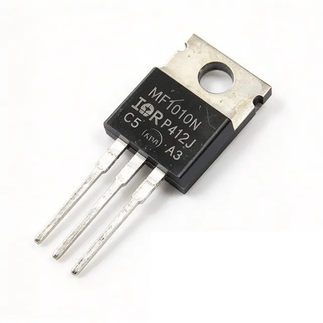
IRF1010NPBF - 55V 85A N-Channel Power MOSFET | Infineon
The Infineon IRF1010NPBF is a 55 V N-channel HEXFET power MOSFET rated for 85 A drain current at a case temperature of 25C, 180 W power dissipation (Tc), and an ultra-low on-resistance of 11 mOhm, housed in the industry-standard through-hole TO-220AB package. A power MOSFET is a voltage-controlled semiconductor switch used to regulate or switch high currents in power management systems. Within the component hierarchy, it sits under transistor > field-effect transistor (FET) > MOSFET > power MOSFET, and it forms the switching element of power supplies, motor drives, and DC-DC converters. The IRF1010NPBF belongs to Infineon (formerly International Rectifier) HEXFET family, one of the most widely second-sourced power MOSFET platforms in the industry. Key features include a 55 V drain-to-source breakdown voltage, 11 mOhm maximum on-resistance at 10 V gate drive, and approximately 80 nC total gate charge for efficient gate-drive design. The planar cell structure provides a wide safe operating area (SOA), and the device is qualified according to JEDEC standards for the industrial market, per the manufacturer datasheet. The advanced process technology achieves extremely low on-resistance per unit silicon area, combining fast switching with a ruggedized device design. Infineon positions this generation of planar MOSFETs for applications switching below 100 kHz, where the planar structure delivers robust avalanche and dv/dt capability that newer trench devices may not match. Typical applications include DC motor control and H-bridge legs, switching power supplies and DC-DC converters, high-current UPS and inverter stages, and battery-powered industrial equipment. The through-hole TO-220AB package simplifies prototyping, heatsink attachment, and high-power thermal design. A key design consideration: at high currents, conduction losses dominate (I^2 x Rds(on)); at 85 A the device dissipates roughly 70 W as an estimate (85A squared times 0.011 Ohm), so a substantial heatsink and low-thermal-resistance mounting are mandatory. Optimize gate drive at 10 V to guarantee the specified Rds(on). This page synthesizes distributor pricing, drop-in alternatives, pinout, comparison tables, and practical design notes not found in the manufacturer datasheet.
IRF1010NPBF-VB - 55V 85A N-Channel Power MOSFET | VBsemi
The VBsemi IRF1010NPBF-VB is a single N-channel HEXFET power MOSFET rated 55 V drain-source voltage, 85 A continuous drain current (at Tc) and 180 W power dissipation (at Tc), housed in a through-hole TO-220AB package. It is a voltage-driven, high-current switching transistor implemented with an advanced planar cell process for low on-resistance and rugged switching performance. A power MOSFET is a voltage-controlled semiconductor switch used at the top of the power-device hierarchy (MOSFET -> power transistor -> power management -> semiconductor). Unlike bipolar junction transistors, MOSFETs are driven by gate voltage rather than base current, giving very high input impedance, fast switching and low drive power. The IRF1010 family belongs to the industry-standard IRF TO-220 through-hole series, which remains one of the most widely second-sourced power MOSFET footprints in the industry. Key features include a 55 V VDSS breakdown rating for 12 V and 24 V bus systems, an on-resistance of approximately 14 mOhm that minimizes conduction losses at high current, a total gate charge of about 80 nC, and the Pb-free RoHS-compliant suffix (PBF) construction. The planar cell structure gives a wide safe operating area, and the device is optimized for switching frequencies below 100 kHz. Technically, the device uses an enhancement-mode N-channel vertical structure with a source-body short that eliminates the parasitic bipolar action, making it rugged against dV/dt events. Gate-source voltage is limited to plus/minus 20 V. The through-hole TO-220AB package offers easy mounting on a heatsink, supporting the full 180 W dissipation rating at case temperatures controlled to 25 C. Typical applications include DC motor drives, high-current switching power supplies, UPS inverters, battery-management switching stages, and automotive-adjacent industrial controllers where a robust, repairable through-hole power switch is preferred. When designing, mount the TO-220AB tab to a properly sized heatsink; at 85 A the conduction loss alone is roughly 100 W (I2 x R = 85^2 x 0.014 Ohm), so real designs must derate or parallel devices. Drive the gate with at least 10 V to fully enhance the channel and minimize RDS(on). This page synthesizes distributor pricing, drop-in cross-references, and practical design notes not found in the manufacturer datasheet, with verified data as of 2026-10-20.
IRF1010NSTRLPBF - 55V 85A N-Channel MOSFET D2PAK | Infineon
The Infineon IRF1010NSTRLPBF is an N-channel enhancement-mode power MOSFET rated at 55 V drain-source voltage, 85 A continuous drain current at Tc, and 180 W power dissipation at Tc, housed in a surface-mount D2PAK (TO-263AB) package with 11 mOhm maximum on-state resistance. It is manufactured on International Rectifier (now Infineon) Advanced Process Technology and supplied in lead-free, RoHS-compliant Tape and Reel packaging. A power MOSFET is a voltage-controlled semiconductor switch used inside power management systems to regulate, convert, and route electrical energy. Within the component hierarchy, the IRF1010NSTRLPBF belongs to the discrete transistor family, specifically the single N-channel MOSFET group under discrete semiconductors, and serves as the switching or rectifying element in DC-DC converters, motor drives, and load-switch circuits. Key features include the 55 V Vdss rating suitable for 12 V and 24 V bus systems, the very low 11 mOhm rDS(on) that minimizes conduction losses at high current, and a 175 C maximum junction temperature rating that supports demanding thermal environments. The device offers fast switching speed, low gate charge typical of the IRF1010 family (approximately 80 nC), and avalanche energy capability for robust operation in inductive switching circuits. Technically, the device uses the HEXFET cell architecture with an advanced process that reduces on-resistance per silicon area, allowing a D2PAK footprint to handle tens of amperes when the drain tab is soldered to a adequately sized copper pour. Gate drive at 10 V achieves full enhancement; logic-level drive is not specified, so a proper gate driver or totem-pole stage is recommended for PWM converters. Typical applications include synchronous rectification in high-output server and telecom DC-DC converters, motor control bridges in power tools and robotics, battery protection and load switches in 12 V and 24 V industrial systems, and switching regulators in welding and lighting equipment. Design consideration: at high continuous currents, conduction loss (I^2 x rDS(on)) dominates; for example, estimated dissipation at 30 A is about 9.9 W, so PCB thermal design with generous drain-tab copper is essential. This page synthesizes distributor pricing, drop-in alternatives, pinout data, and practical design notes not found in the manufacturer datasheet.
IRF1010ZPBF - 55V 75A N-Channel MOSFET TO-220AB | Infineon
The Infineon IRF1010ZPBF is an N-channel HEXFET power MOSFET rated at 55 V drain-source voltage, 75 A continuous drain current at Tc=25C, and 140 W power dissipation at Tc=25C, housed in the industry-standard TO-220AB through-hole package. It features an ultra-low on-state resistance of approximately 7.5 mOhm typical and a total gate charge of around 63 nC, making it a high-efficiency switching transistor for power conversion stages. A power MOSFET is a voltage-controlled semiconductor switch used in the power-management layer of electronic systems, sitting between gate drivers and the load in the hierarchy of power semiconductors. Unlike bipolar transistors, MOSFETs switch with essentially no DC gate current, which simplifies drive circuitry and improves efficiency in switched-mode power supplies, motor drives, and DC-DC converters. Key features of the IRF1010ZPBF include advanced process technology for extremely low RDS(on) per silicon area, a high 175C maximum junction temperature, fast switching speed, and improved repetitive avalanche rating. The Z suffix denotes the low-charge gate design family, reducing driver losses in high-frequency switching. The PBF suffix indicates a lead-free, RoHS-compliant construction suitable for global markets. Technically, the device uses Infineon HEXFET multi-cell geometry with a trench-based advanced process that minimizes conduction losses: at 7.5 mOhm and 75 A, conduction loss is roughly 42 W at full rated current, so designers typically operate well below this in thermally constrained enclosures. The low gate charge supports efficient operation with common gate-driver ICs in the tens to hundreds of kilohertz range. Typical applications include DC motor control and H-bridge legs, switching regulators, battery-powered inverters, UPS output stages, and automotive or industrial relay replacement circuits. High current rating and wide distributor availability make it a common choice for repair and maintenance of legacy power boards. A key design consideration is thermal management: the TO-220AB package requires a heatsink or generous copper area above approximately 10 W of dissipation, and gate-drive resistors should be sized to control switching-edge ringing without slowing transitions excessively. This page synthesizes distributor pricing context, drop-in alternatives, practical design notes, and a parametric comparison table not found in the manufacturer datasheet.
IRF1010ZSTRLPBF - 55V 75A N-Channel MOSFET D2PAK | Infineon
The Infineon IRF1010ZSTRLPBF is an N-channel HEXFET power MOSFET rated at 55 V drain-source voltage, 75 A continuous drain current (Tc), and 140 W power dissipation (Tc), housed in a surface-mount D2PAK (TO-263) package. Per distributor data it features an ultra-low on-resistance of 7.5 mOhm and a total gate charge of 63 nC. A power MOSFET is a voltage-controlled semiconductor switch that regulates or switches electrical power in circuits. Within the power-management hierarchy, it sits alongside IGBTs and thyristors as a discrete power transistor: a MOSFET is a type of transistor, which is a type of semiconductor device used in switch-mode power supplies, motor drives, and load-switching stages. The N-channel enhancement-mode construction means the device conducts when the gate is driven positive relative to the source, offering lower on-resistance than equivalent P-channel parts. Key features include Infineon advanced process technology (originally International Rectifier HEXFET), extremely low on-resistance per silicon area, a 175 C maximum junction operating temperature, fast switching speed, and an improved repetitive avalanche rating. These characteristics combine high efficiency with robustness in hard-switching and inductive-load environments. Technically, the low RDS(on) of 7.5 mOhm minimizes conduction losses: Estimated: at 75 A, conduction loss is I2 x R = 75 x 75 x 0.0075 = about 42 W, so thermal design and copper pours on the drain tab are essential at high duty cycles. The low 63 nC gate charge reduces gate-drive losses in high-frequency converters, allowing smaller gate drivers and higher switching frequencies. Typical applications include DC-DC converters and point-of-load power supplies, motor control and PWM motor drives, battery management and reverse-polarity protection in 12 V to 48 V systems, and high-current load switches in industrial and automotive-adjacent equipment. A key design consideration: the D2PAK drain tab is electrically connected to the drain, so PCB copper area under the tab is both the main thermal path and a high-voltage node; maintain proper creepage and use multiple thermal vias. This page synthesizes distributor pricing data, drop-in alternatives, design notes, and a parametric comparison not found together in the manufacturer datasheet.
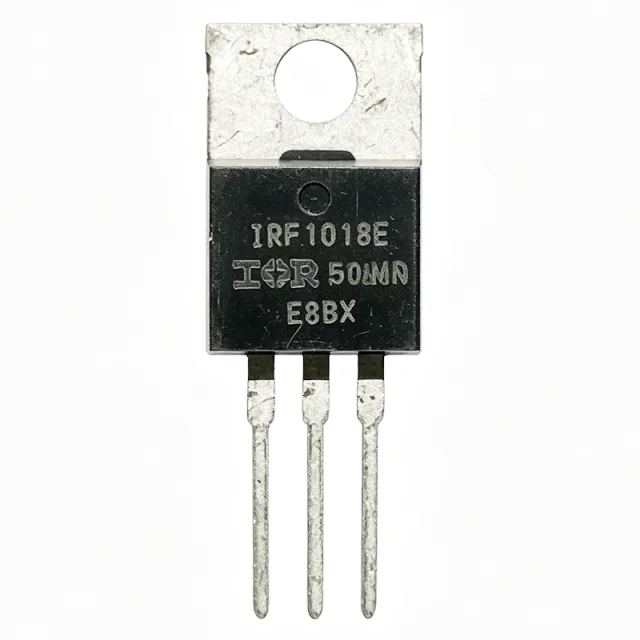
IRF1018EPBF - 60V 79A 8.4mOhm N-Ch HEXFET MOSFET | Infineon
The Infineon IRF1018EPBF is a 60 V single N-channel HEXFET power MOSFET rated for 79 A continuous drain current at Tc, with an ultra-low on-resistance of 8.4 mOhm typical and a total gate charge of 46 nC, housed in the industry-standard TO-220AB through-hole package. Originally released by International Rectifier and now part of Infineon's HEXFET portfolio, this device is qualified to JEDEC standards and optimized for 10 V gate drive, making it ideal for high-efficiency synchronous rectification in switched-mode power supplies (SMPS), motor drives, and PWM control applications. A power MOSFET (Metal-Oxide-Semiconductor Field-Effect Transistor) is a voltage-controlled semiconductor switch used to efficiently commutate current between the drain and source terminals. Power MOSFETs belong to the broader family of discrete transistors, which sit under discrete semiconductors and ultimately the semiconductor device hierarchy. N-channel enhancement-mode MOSFETs like the IRF1018EPBF are the dominant switch choice for low-voltage (<=100 V) synchronous rectification, low-side buck switches, and DC motor control because they offer fast switching, simple gate drive (10 V typical), and low conduction loss. Compared with P-channel MOSFETs and bipolar junction transistors (BJTs), N-channel MOSFETs deliver lower Rds(on) per unit silicon area and require only a positive gate-source voltage to turn on. Key features include 8.4 mOhm Rds(on) at Vgs=10 V, 46 nC total gate charge (Qg), and a maximum continuous drain current of 79 A at 25 C case temperature. The TO-220AB package is rated for 110 W power dissipation at Tc=25 C and provides a thermal resistance (junction-to-case) suitable for attaching a clip-on or PCB-mounted heatsink. The device is optimized for 10 V Vgs drive, which simplifies interface to standard gate-driver ICs and most microcontrollers with logic-level PWM outputs. Technically, the IRF1018EPBF uses Infineon's proprietary HEXFET silicon trench technology, which achieves low specific on-resistance (Rds(on) x area) and high avalanche ruggedness. Its low Qg (46 nC) and Qgd values reduce switching losses and enable operation above 100 kHz in synchronous-rectifier positions. The optimized body diode supports continuous-conduction-mode (CCM) PFC and synchronous-buck topologies without requiring an external anti-parallel diode. Typical applications include high-efficiency synchronous rectification in server and telecom SMPS, low-side switch in DC-DC buck converters, brushless DC (BLDC) motor drives, Class-D audio output stages, industrial PWM motor control, and battery protection/load switching in 12 V/24 V systems. The 60 V rating also provides ample margin for 48 V telecom rails and transient-prone automotive 24 V environments. When designing with the IRF1018EPBF, ensure adequate heatsinking at high continuous current: at 79 A the device dissipates roughly 52 W (I^2 * Rds(on)) and the TO-220AB junction-to-ambient thermal resistance typically forces a clip-on heatsink for sustained operation above 30 A. A 10 V gate drive is required; logic-level (4.5 V) gate drive will substantially raise Rds(on) and is not recommended. This page synthesizes distributor pricing, drop-in alternatives from same-brand and cross-brand sources, and practical design notes not found in the manufacturer datasheet alone.

IRF1310NPBF - 100V 42A N-Channel HEXFET MOSFET | Infineon
The Infineon IRF1310NPBF is an N-channel power MOSFET rated at 100 V VDS, 42 A continuous drain current (at TC) and 160 W power dissipation in a TO-220AB through-hole package. Built on Infineon's HEXFET power MOSFET process, it delivers 36 mOhm maximum on-resistance at VGS=10V and a total gate charge of 73.3 nC, making it well suited for high-current DC switching applications. A power MOSFET is a voltage-controlled semiconductor switch that uses an insulated gate (typically oxide) to modulate current flow between drain and source terminals. The HEXFET family, originally developed by International Rectifier (now part of Infineon), uses a cellular planar stripe structure with thousands of parallel MOSFET cells on a single die. Within the broader semiconductor taxonomy, this places the IRF1310NPBF in the power MOSFET > discrete transistor > discrete semiconductor hierarchy. The device is characterized by very low on-resistance per unit of silicon area, fast switching speed, and excellent thermal performance when mounted to a heatsink. Key features include 100 V drain-source breakdown voltage, 42 A continuous drain current at TC=25C, 36 mOhm maximum static drain-source on-resistance (RDS(on)) at VGS=10V and ID=25A, a 175C maximum junction temperature, and an avalanche-energy-rated body diode. The TO-220AB package provides a low thermal resistance path (junction-to-case) and supports through-hole mounting with a tab that doubles as the drain terminal, enabling direct mechanical attachment to a heatsink. From a design perspective, the IRF1310NPBF's low gate charge (73.3 nC) and standard 10V gate drive simplify driver selection, while the low RDS(on) minimizes conduction losses in high-current loops. Designers should observe safe operating area (SOA) limits, especially during switching transients, and provide adequate heatsinking at full 42A loads. Typical applications include switched-mode power supplies (SMPS), DC motor drives, uninterruptible power supplies (UPS), automotive ignition and fuel-injection switching, solenoid drivers, audio amplifier output stages, and high-current DC load switches. The combination of high current rating and TO-220 form factor makes it a workhorse for industrial and hobbyist power electronics. When designing with this part, ensure VGS drive swings to 10V for full enhancement; logic-level signals (3.3V or 5V) will not fully turn on the device. Always check the SOA graph in the manufacturer datasheet for your specific VDS, ID, and pulse duration, and add a gate-source resistor (typically 10-100 ohm) to suppress ringing on long gate traces.

IRF1310NSTRLPBF - 100V 42A N-Channel MOSFET | Infineon D2PAK
The Infineon IRF1310NSTRLPBF is an N-channel power MOSFET rated at 100 V VDS and 42 A continuous drain current, housed in a surface-mount D2PAK (TO-263AB) package. It features an ultra-low on-resistance of 36 mOhm maximum and a total gate charge of 73.3 nC, originally developed by International Rectifier using the advanced IR MOSFET process technology. An N-channel power MOSFET is a voltage-controlled semiconductor switch in which a positive gate-to-source voltage creates a conductive channel between drain and source. N-channel MOSFETs are preferred over P-channel variants for high-current switching because electrons have higher mobility than holes, yielding lower RDS(on) per unit silicon area. Power MOSFETs sit within the discrete semiconductor hierarchy: MOSFET -> transistor -> discrete semiconductor -> semiconductor, and are the workhorse switching element in switch-mode power supplies (SMPS), motor drives, and DC-DC converters operating from a few amps to hundreds of amps. Key features include 100 V drain-source breakdown voltage, 42 A continuous drain current at TC, an exceptionally low 36 mOhm maximum RDS(on) at VGS = 10 V, and avalanche-rated ruggedness typical of the IRF1310N generation. The D2PAK surface-mount package provides a thermal resistance of around 40 C/W junction-to-case, enabling dissipation up to 160 W when mounted on a properly designed PCB copper area. The device is fully lead-free and RoHS compliant. The IRF1310N utilizes Infineon's HEXFET power MOSFET process with a vertical DMOS structure, where current flows vertically through the die from the top drain contact (bonded to the D2PAK tab) to the source bond wires on top. This architecture delivers the high current density and low RDS(on) needed for synchronous rectification and high-side switch positions. The 73.3 nC gate charge enables moderate switching frequencies in the 100-500 kHz range without excessive gate-drive losses. Typical applications include secondary-side synchronous rectification in 48 V telecom converters, high-current DC motor drives, uninterruptible power supply (UPS) battery switches, automotive 12 V/24 V load controllers, and Class-D audio amplifier output stages. The 100 V rating provides ample margin above 48 V telecom rails and 24 V industrial buses. When designing with this MOSFET, pay particular attention to gate-drive voltage: full enhancement (lowest RDS(on)) requires VGS of 10 V, while logic-level thresholds around 4.5 V are not supported. Use a dedicated gate-driver IC rather than a microcontroller GPIO to achieve fast switching transitions and minimize switching losses. This page synthesizes distributor pricing, drop-in alternatives, and practical design notes not found in the manufacturer datasheet.

IRF1405PBF - 55V 169A N-Channel HEXFET MOSFET | Infineon
The Infineon IRF1405PBF is a 55V N-channel HEXFET power MOSFET rated for 169A continuous drain current (Tc) and 330W power dissipation in a TO-220AB through-hole package. It delivers an extremely low typical on-resistance of 5.3 mOhm, fast switching speed, and a 175C maximum junction temperature, making it one of the most efficient planar-cell MOSFETs in its class. The PbF suffix denotes lead-free terminal finish compliant with RoHS. A power MOSFET (Metal-Oxide-Semiconductor Field-Effect Transistor) is a voltage-controlled semiconductor switch used to efficiently route or modulate high currents in power-conversion circuits. N-channel MOSFETs conduct when the gate is pulled above the source by the threshold voltage (Vth). Within the broader taxonomy, the IRF1405 belongs to the HEXFET family -> power MOSFET -> discrete semiconductor -> active electronic component. The IRF1405PBF uses Stripe Planar cell construction to minimize R_DS(on) per silicon area while preserving a wide safe operating area. Key differentiating specifications include the 169A continuous drain current at 25C case temperature, 330W maximum power dissipation, gate threshold of 2.0V to 4.0V, and avalanche-rated construction for repetitive unclamped inductive switching. The TO-220AB package provides a low thermal resistance path and is widely accepted by industrial and automotive customers. The planar cell structure optimizes switching behavior below 100 kHz, the typical regime for motor drives, solenoid drivers, and DC-DC converters. Architecturally, the IRF1405PBF uses Infineon's mature HEXFET stripe planar process, balancing low R_DS(on), rugged avalanche capability, and fast body-diode recovery. This positions it well for high-current switching where conduction losses dominate and switching frequency remains moderate. Compared with trench MOSFETs of similar ratings, the planar structure generally offers wider SOA and higher avalanche energy, at the cost of slightly higher R_DS(on) per die area. Typical applications include anti-lock braking systems (ABS), electric power steering (EPS), DC motor control, solenoid drivers, power OR-ing, battery protection, and high-current DC-DC converters. Automotive and industrial designers favor the TO-220AB footprint for its thermal performance and mechanical ruggedness in harsh environments. When designing with the IRF1405PBF, ensure that the gate drive voltage comfortably exceeds Vgs(th) under all temperature conditions, and size the heatsink so that junction temperature stays below 150C at worst-case load. A low-impedance gate-drive loop is essential to avoid parasitic turn-on in bridge topologies. This page synthesizes Infineon datasheet specifications, distributor pricing, drop-in alternatives in TO-220AB, and practical thermal and gate-drive design notes not found in any single manufacturer source.

IRF1407PBF - 75V 130A N-Channel HEXFET MOSFET | Infineon
The Infineon IRF1407PBF is an N-channel 75V HEXFET power MOSFET rated for 130A continuous drain current and 330W power dissipation in a TO-220AB through-hole package. It features an extremely low typical on-resistance of 7.8 mOhm at VGS=10V, a 175C maximum junction temperature, fast switching speed, and an improved repetitive avalanche rating. A power MOSFET (Metal-Oxide-Semiconductor Field-Effect Transistor) is a voltage-controlled semiconductor switch used to switch or amplify electrical signals in power-electronics applications. The N-channel enhancement-mode variant requires a positive gate-source voltage to turn on and is the dominant topology for low-voltage, high-current switching because electron mobility in the channel is roughly 2-3x higher than hole mobility, yielding lower RDS(on) for a given silicon area. Within the broader taxonomy, MOSFETs are members of the power transistor family alongside IGBTs and BJTs, sitting under the discrete-semiconductor hierarchy. Key electrical strengths of the IRF1407PBF include its industry-leading 7.8 mOhm RDS(on) at 10V VGS, which directly minimizes conduction loss in high-current paths, and a low typical gate charge of 160 nC that enables fast switching transitions at high frequencies. The 175C rated junction temperature provides substantial thermal headroom for harsh industrial environments, and the fully avalanche-rated design allows unclamped inductive switching within the published repetitive-avalanche energy limit. The device is built on Infineon's advanced stripe-planar HEXFET process, where the source metal is arranged in stripes over the silicon to maximize cell density and minimize cell resistance. This architecture, combined with the company's latest processing techniques, achieves an unusually low figure of merit (FOM = RDS(on) x Qg) for a 75V part, making the IRF1407PBF well suited to high-current synchronous-rectifier and motor-drive stages where both conduction and switching losses matter. Typical applications include high-current DC motor drives in industrial automation, synchronous-rectifier stages in 48V telecom and server power supplies, low-voltage high-current buck converters for battery management, solenoid and relay drivers, and uninterruptible power supply (UPS) battery switches. The 75V rating also gives comfortable margin in 24V and 48V automotive and telecom bus systems. When designing with the IRF1407PBF, ensure the gate driver can source and sink at least 1-2A to charge and discharge the 160 nC gate charge within the target switching time, and observe the SOA curve in the manufacturer datasheet for linear-mode or hot-swap operation. Use a low-impedance gate-source connection with a pull-down resistor to prevent inadvertent turn-on from Miller current. This page synthesizes distributor pricing, drop-in alternatives, and practical design notes not found in the manufacturer datasheet, including a side-by-side comparison with same-package TO-220AB alternates.
IRF150DM115XTMA1 - 150V OptiMOS 5 N-FET | Infineon
The Infineon IRF150DM115XTMA1 is an N-channel power MOSFET built on Infineon's OptiMOS 5 process and housed in the ultra-thin, double-side-cooled DirectFET package. It is rated for 150 V drain-source voltage and is targeted at high power-density designs where low parasitic inductance and a slim profile are essential, such as photovoltaic optimisers, cordless power tools, and high-current motor control stages. An N-channel MOSFET (Metal-Oxide-Semiconductor Field-Effect Transistor) is a voltage-controlled device used to switch or amplify signals in power electronics. In the power hierarchy it sits under the broader categories of discrete semiconductor -> transistor -> FET -> power MOSFET. OptiMOS 5 is Infineon's fifth-generation 150 V trench technology, which combines a very low on-resistance per area with a low gate charge to deliver an excellent FOM (RDS(on) x QG figure of merit). Key specifications include an exceptionally low on-resistance per die area, low gate charge, 100% avalanche-tested ruggedness, and a normal-level (standard) gate threshold that is compatible with typical 12 V gate-drive signals. The DirectFET package removes the internal wire bonds used in conventional DPAK/TO-220 parts, which dramatically lowers source-inductance and improves both switching speed and thermal performance. Because the package can be cooled from both top and bottom, system designers can extract more power from the same PCB footprint. Typical applications include synchronous rectification stages in telecom and server DC-DC bricks, battery protection and hot-swap in 48 V e-mobility tools, photovoltaic module-level power electronics, and the high-side/low-side switches in BLDC motor drives. The combination of low RDS(on) and DirectFET thermal performance makes it attractive where board area is at a premium. When designing with this part, ensure the gate-drive voltage is high enough to fully enhance the channel (10 V recommended) and that the layout keeps the high-current loop area as small as possible to leverage the package's low parasitic inductance. This page combines distributor pricing, drop-in alternatives, and practical design notes not found in the manufacturer datasheet alone.

IRF150P220AKMA1 - 150V 203A StrongIRFET Power MOSFET | Infineon
The Infineon IRF150P220AKMA1 is a 150V N-channel StrongIRFET power MOSFET delivering 203A continuous drain current (Tc) with an ultra-low 2.7 mOhm maximum on-resistance, housed in a TO-247-3 through-hole package. As part of Infineon's StrongIRFET family, this device is engineered for high-current, low-loss switching in demanding power conversion applications where thermal robustness and avalanche ruggedness are critical. What is a StrongIRFET power MOSFET? A StrongIRFET is Infineon's portfolio of high-performance N-channel power MOSFETs optimized for low RDS(on) per unit silicon area, fast switching, and high avalanche energy capability. Power MOSFETs belong to the broader discrete semiconductor hierarchy: MOSFET -> transistor -> discrete semiconductor -> semiconductor. StrongIRFET devices typically use trench-gate technology to minimize conduction and switching losses, making them the preferred choice for high-current DC-DC converters, motor drives, and synchronous rectification where efficiency directly impacts system thermal budget. The IRF150P220AKMA1 features 150V drain-source voltage rating, 2.7 mOhm max RDS(on) at VGS=10V, and 203A continuous drain current at 25C case temperature, with pulsed capability well above that. The TO-247-3 package provides 556W power dissipation at Tc, with thermal resistance (RthJC) optimized for high-current switching. The device also supports avalanche operation and is qualified for industrial-grade temperature ranges. Typical applications include high-current synchronous rectification in telecom and server power supplies, brushless DC motor drives, solar inverters, industrial SMPS, and uninterruptible power supplies (UPS). The wide SOA allows safe linear-mode operation during transients. When designing with this device, ensure gate drive voltage reaches 10V for full RDS(on) spec. PCB layout must minimize source-inductance loop area to prevent voltage spikes during switching. Mount with proper torque on TO-247 heatsink for thermal performance.
IRF2805PBF - 55V 175A N-Channel HEXFET MOSFET | Infineon
The Infineon IRF2805PBF is an N-channel HEXFET power MOSFET rated at 55 V VDS and 175 A continuous drain current (with 75 A at Tc), housed in a TO-220AB through-hole package. It utilizes advanced process technology to achieve a maximum on-resistance of 4.7 mOhm at VGS = 10 V, with a total gate charge of 150 nC and a power dissipation of 330 W at Tc. An N-channel power MOSFET is a voltage-controlled semiconductor switch that conducts current between drain and source when a positive gate-to-source voltage is applied. It belongs to the power MOSFET family within the broader class of discrete semiconductors and is widely used as the active switching element in DC-DC converters, motor drives, and power management circuits where high efficiency and fast switching are required. Key features of the IRF2805PBF include a 175 °C maximum junction operating temperature, fast switching speed, and an improved repetitive avalanche rating for rugged inductive switching. The device offers exceptionally low on-resistance per silicon area, making it one of the most efficient 55 V-class TO-220 MOSFETs for high-current applications. The threshold voltage is specified at 4 V, with a guaranteed low on-resistance at VGS = 10 V. The IRF2805PBF is specifically designed for automotive and heavy industrial applications, combining HEXFET power MOSFET technology with a robust TO-220AB package that supports through-hole mounting and efficient thermal dissipation via the metal tab. Its low RDS(on) minimizes conduction losses, while the fast body diode and avalanche capability improve reliability under harsh switching transients. Typical applications include high-current DC motor drives, automotive power switching (battery management, ignition, and load control), uninterruptible power supplies (UPS), high-power synchronous rectifiers, welding equipment, and industrial inverters. The 55 V drain-to-source rating also makes it suitable for 12 V and 24 V automotive bus systems. When designing with this device, ensure that the gate drive voltage reaches at least 10 V to achieve the rated 4.7 mOhm RDS(on). Proper heatsinking is critical because, at 75 A continuous, conduction losses can exceed 25 W; the TO-220AB tab should be mounted to a chassis or external heatsink with thermal compound. This page synthesizes distributor pricing, drop-in alternatives, and practical design notes not found in the manufacturer datasheet, helping engineers select, source, and integrate the IRF2805PBF with confidence.

IRF2907ZSTRLPBF - 75V 170A N-Ch HEXFET MOSFET D2PAK | Infineon
The Infineon IRF2907ZSTRLPBF is an N-channel HEXFET power MOSFET rated for 75 V V(BR)DSS, 170 A continuous drain current (silicon-limited) and an ultra-low on-resistance of 3.5 mOhm (typical) to 4.5 mOhm (max at VGS = 10 V), packaged in a surface-mount D2PAK (TO-263AB) with tape-and-reel packaging. It belongs to Infineon's IR MOSFET family and is built on advanced process technology that yields extremely low RDS(on) per silicon area while preserving a 175 °C maximum junction operating temperature. A power MOSFET (Metal-Oxide-Semiconductor Field-Effect Transistor) is a voltage-controlled majority-carrier switch that conducts current between drain and source when a sufficient gate-source voltage is applied. Power MOSFETs are the workhorse switching devices in the discrete-semiconductors hierarchy, sitting below IGBTs and above signal-level FETs. Within Infineon's portfolio the IRF2907Z family targets 12 V/24 V/48 V automotive and industrial switching rails where ultra-low conduction loss and high current pulse capability are required. Key features include 4.5 mOhm max RDS(on) at VGS = 10 V, repetitive avalanche rating up to TJ(max), fast switching speed for high-frequency PWM converters, and lead-free / RoHS-compliant construction. The D2PAK package provides a low thermal resistance path via its exposed metal tab, allowing the die to dissipate 300 W (at TC = 25 °C) when properly soldered to a PCB copper pad. The S suffix in the part number designates tape-and-reel orientation, while the LPBF suffix confirms lead-free termination. Typical applications include high-current DC motor drives in automotive and industrial systems, synchronous-rectifier low-side switches in 24 V to 48 V buck converters, battery protection circuits for 12 V/24 V lead-acid and Li-ion packs, and solenoid/relay drivers. Designers also use it in audio amplifier output stages, uninterruptible power supplies (UPS), and welding inverter half-bridge switches where the avalanche rating provides additional safety margin during turn-off transients. When designing with this MOSFET, calculate conduction loss as P = I_DS(RMS)^2 * RDS(on) and switching loss separately using Qg and the gate-driver current. The exposed tab must be soldered to a minimum 1 oz copper area of at least 1 square inch to keep the junction below 150 °C at full load. Heatsinking is not required at moderate currents, but at 100 A continuous the PCB copper itself becomes the heatsink.

IRF3007STRLPBF - 75V N-Channel MOSFET, 62A, D2PAK | Infineon
The Infineon IRF3007STRLPBF is an N-channel enhancement-mode power MOSFET rated at 75 V V(BR)DSS, 62 A continuous drain current (Tc), and 120 W power dissipation (Tc), housed in a surface-mount D2PAK (TO-263) package with tape-and-reel packaging. Built on Infineon's advanced HEXFET process, it delivers an ultra-low on-resistance of 12.6 mΩ (typical at VGS = 10 V) and supports switching frequencies suitable for high-current DC-DC converters, motor drives, and synchronous rectification. What is a power MOSFET? A power MOSFET (Metal-Oxide-Semiconductor Field-Effect Transistor) is a voltage-controlled semiconductor switch used to handle high currents and voltages with minimal conduction loss. As a member of the N-channel enhancement-mode family, the IRF3007STRLPBF turns on when a positive gate-to-source voltage exceeds its threshold, allowing current to flow from drain to source. Within the power-management hierarchy, it sits between signal-level logic MOSFETs and IGBTs (Insulated Gate Bipolar Transistors), offering the best balance of low on-resistance and moderate switching speed for sub-100 V applications. Key specifications include a drain-to-source breakdown voltage of 75 V, continuous drain current of 62 A at 25 °C case temperature, pulsed drain current handling of 250 A, and a maximum junction temperature of 175 °C. The 12.6 mΩ typical R_DS(on) at VGS = 10 V minimizes conduction losses, while the low gate charge (typically 110 nC total) and fast switching characteristics support efficient high-frequency operation. The D2PAK package provides a low thermal resistance of 40 °C/W junction-to-case, enabling direct PCB heatsink mounting for high-power designs. Typical applications include industrial motor drives, synchronous rectification in switch-mode power supplies, DC-DC converter high-side switches, battery management systems for 12 V/24 V/48 V rails, and automotive solenoid and relay drivers. The 175 °C maximum junction temperature and avalanche-rated ruggedness make it suitable for harsh-environment designs where repetitive avalanche events may occur. When designing with this device, ensure the gate drive voltage reaches at least 10 V for full enhancement and minimum R_DS(on). Use a gate resistor (typically 10-100 Ω) to control switching speed and limit ringing, and provide adequate copper pours or an external heatsink to keep junction temperature below 150 °C for reliable long-term operation. This page synthesizes distributor pricing, drop-in alternatives, and practical design notes not found in the manufacturer datasheet alone.