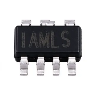
AP63203WU-7 - 2A, 32V Synchronous Buck, 3.3V Fixed Output | Diodes Inc
Référence : AP63203WU-7 ✓ Actif| Qté | Prix unitaire | Total |
|---|---|---|
| 1 | $0.76 | $0,76 |
| 10 | $0.68 | $6,80 |
| 100 | $0.55 | $55,00 |
| 500 | $0.46 | $230,00 |
| 1 000 | $0.39 | $390,00 |
| 3 000 | $0.32 | $960,00 |
AP63203WU-7 Présentation
What is a synchronous buck converter? A synchronous buck (step-down) converter is a type of switching voltage regulator that uses two MOSFETs (high-side and low-side) to convert a higher DC input voltage to a lower DC output voltage. Synchronous buck designs replace the traditional Schottky rectifier with a low-side MOSFET, improving efficiency especially at high loads. Buck converters sit within the power management IC hierarchy: switching regulator > DC-DC converter > power management IC > semiconductor. They are preferred over linear regulators when VIN-VOUT differentials exceed 1-2V due to dramatically higher efficiency.
Key features of the AP63203WU-7 include an ultra-low 22 uA quiescent current, 0.8V +/-1% reference voltage accuracy, fixed 3.3V output, and 1.1 MHz switching frequency. Enhanced EMI performance is achieved through proprietary switching techniques. The 1.1 MHz switching frequency enables small external LC filters. Cycle-by-cycle peak current limiting, hiccup mode short-circuit protection, and thermal shutdown provide robust fault handling.
The AP63203 employs constant-on-time (COT) control architecture, delivering fast transient response without requiring external loop compensation components. The integrated MOSFETs eliminate the need for an external Schottky diode. The high-side P-channel MOSFET blocks inrush current at startup.
Typical applications include industrial 24V bus distributed power systems, USB Type-C PD adapters, home automation IoT nodes, white goods control boards, and FPGA/CPLD auxiliary rails. The wide 3.8V-32V input tolerates voltage transients commonly found in industrial and PoE applications.
When designing with this device, place the input capacitor (minimum 4.7 uF ceramic) as close as possible to VIN and GND pins. The output inductor (typically 2.2 uH) and output capacitor (22 uF minimum ceramic) form the FBAR network that sets ripple performance. The EN pin can be tied to VIN for automatic startup or driven by a GPIO for sequencing.
This page synthesizes distributor pricing, drop-in alternatives, and practical design notes not found in the manufacturer datasheet.
Alternatives de remplacement direct pour AP63203WU-7 — même boîtier, compatible broche à broche. Les références à boîtier différent nécessitant une retouche du PCB sont exclues.
Variantes de cette série
Modèles de la même série directement compatibles avec AP63203WU-7 (même facteur de forme et même empreinte) — différant par Package, Protection Features, Quiescent Current, Switching Frequency, Topology.
Outil de comparaison rapide — sélectionnez des références alternatives pour une comparaison côte à côte :
AP63205WU-7
✅ Remplacement direct✓ En stock
$0.2036 / unité
Voir la fiche technique →AP63201WU-7
✅ Remplacement direct✓ En stock
$0.45 / unité
Voir la fiche technique →AP63200WU-7
✅ Remplacement direct✓ En stock
$0.49 / unité
Voir la fiche technique →TPS62177DQCR
✅ Remplacement direct📋 Alternative de référence (hors catalogue)
MP2155GQ-P
✅ Remplacement direct📋 Alternative de référence (hors catalogue)
AP63203WU-7 Valeurs maximales et caractéristiques électriques
| Topologie | Synchronous Buck (Step-Down) |
| Plage de tension d'entrée | 3.8 V to 32 V |
| Tension de sortie | Fixed 3.3 V |
| Continuous Output Current | 2 A |
| Fréquence de commutation | 1.1 MHz |
| High-Side MOSFET Rds(on) | 125 mOhm |
| Low-Side MOSFET Rds(on) | 68 mOhm |
| Courant de repos | 22 uA (ultralow) |
| Reference Voltage Accuracy | 0.8 V +/-1% |
| Light-Load Efficiency (1 mA) | Up to 80% |
| Light-Load Efficiency (5 mA) | Up to 88% |
| Température de fonctionnement | -40C to +85C |
| Boîtier | TSOT-23-6 (Thin SOT-23-6) |
| Type de montage | Surface Mount |
| Enable Input | Yes (EN active-high) |
| Protection Features | Cycle-by-cycle current limit, hiccup mode, thermal shutdown |
| Statut RoHS | Compliant |
Configuration des broches de AP63203WU-7
| Broche 1 | GND — Ground reference |
| Broche 2 | VIN — Input supply voltage (3.8V to 32V) |
| Broche 3 | SW — Switch node - connect to inductor |
| Broche 4 | FB — Feedback sense for output voltage regulation |
| Broche 5 | EN — Enable input (active high) |
| Broche 6 | BST — Bootstrap for high-side gate driver [DATA_NEEDED: per-package exact function] |
Applications typiques
AP63203WU-7 convient pour 6 applications: Industrial 24V Bus Distributed Power, USB Type-C Power Delivery Adapter, Home Automation IoT Sensor Node, White Goods and Appliance Control Board, FPGA/CPLD Auxiliary Rail Supply, Point-of-Sale Terminal Power.
Industrial 24V Bus Distributed Power
The AP63203WU-7's wide 3.8V to 32V input tolerance makes it ideal for industrial 24V bus systems where transients and ripple are common. It converts 24V directly to 3.3V at 2A without a preregulator, delivering up to 88% efficiency at moderate loads and eliminating thermal management challenges. The integrated 125 mOhm/68 mOhm MOSFETs minimize PCB area, while 22 uA quiescent current preserves standby budget. Place a 4.7 uF ceramic input cap close to VIN/GND to absorb bus transients.
Recommandé
USB Type-C Power Delivery Adapter
The AP63203WU-7 fits USB Type-C PD adapter secondary-side regulation where 5-20V input must be stepped to 3.3V rail for MCU and protocol IC. Its 1.1 MHz switching frequency enables small inductor (2.2 uH) and 22 uF ceramic output cap, fitting within compact adapter enclosures. Enhanced EMI reduction meets CISPR 22/32 Class B with simple input filtering. Synchronous rectification eliminates the Schottky diode, reducing BOM cost by approximately $0.05 per unit.
Recommandé
Home Automation IoT Sensor Node
The AP63203WU-7's 22 uA ultralow quiescent current extends battery life in home automation IoT sensor nodes that spend 99% of time in sleep mode. With 80% efficiency at 1 mA and 88% at 5 mA, the device minimizes standby drain while supporting 2A peaks for radio transmissions. The wide 3.8-32V VIN accepts energy-harvested or multi-cell battery inputs directly. Thermal shutdown and hiccup-mode short-circuit protection ensure unattended long-term reliability.
Recommandé
White Goods and Appliance Control Board
White goods control boards operate from rectified 24V or 12V rails with significant motor-induced transients. The AP63203WU-7's 32V maximum input rating tolerates load-dump transients in washing machines, refrigerators, and dishwashers without a TVS clamp. Fixed 3.3V output drives MCU, display, and sensor subsystems at 2A peak load. The TSOT-23-6 package fits within tight control-board layouts, and the -40C to +85C operating range covers appliance environments.
Recommandé
FPGA/CPLD Auxiliary Rail Supply
FPGAs and CPLDs require multiple low-voltage rails (3.3V, 2.5V, 1.8V, 1.2V) generated from a common 5V or 24V input. The AP63203WU-7 provides the 3.3V rail with 1.1 MHz switching that does not couple into a synthesizer's PLL reference. Cycle-by-cycle peak current limit and hiccup-mode protection guard against FPGA in-rush during configuration. The exposed GND pad enables direct thermal dissipation into the inner PCB ground plane.
Recommandé
Point-of-Sale Terminal Power
Point-of-sale (POS) terminals use 24V adapters that must power printers, displays, card readers, and embedded controllers. The AP63203WU-7 converts 24V input to 3.3V at 2A peak for the main processor and connectivity subsystems. The enhanced EMI reduction feature simplifies FCC/CE Class B certification by attenuating switching noise below regulatory thresholds. The fixed 3.3V output eliminates external feedback components, reducing BOM cost in cost-sensitive POS designs.
Recommandé
Récapitulatif des produits recommandés
Données de référence d'ingénierie pour AP63203WU-7 — comparaison, recommandations de conception et informations de conformité.
Guide de sélection
Comparaison avec les alternatives
| Paramètre | Ce produit | AP63205WU-7 | AP63201WU-7 | AP63200WU-7 | TPS62177DQCR | MP2155GQ-P |
|---|---|---|---|---|---|---|
| Package | TSOT-23-6 | TSOT-23-6 - same | TSOT-23-6 - same | TSOT-23-6 - same | TSOT-23-6 - same | TSOT-23-6 - same |
| Brand | Diodes Incorporated | Diodes Incorporated | Diodes Incorporated | Diodes Incorporated | Texas Instruments | MPS |
| Output Voltage | Fixed 3.3V | Fixed 5.0V | Fixed 3.3V | Fixed 3.3V | Fixed 3.3V | Fixed 3.3V |
| Output Current | 2 A | 2 A | 2 A | 2 A | 0.5 A | 1.5 A |
| Input Voltage Range | 3.8 V to 32 V | 3.8 V to 32 V | 3.8 V to 32 V | 3.8 V to 32 V | 4.7 V to 28 V | 4.5 V to 28 V |
| Switching Frequency | 1.1 MHz | 1.1 MHz | 500 kHz | 500 kHz | 1.0 MHz | 1.0 MHz |
| Quiescent Current | 22 uA | 22 uA | 22 uA | 22 uA | 17 uA | 40 uA |
| Light-Load Efficiency | Up to 88% at 5 mA | Up to 88% at 5 mA | Higher (PFM mode) | Up to 88% at 5 mA | Up to 85% at 5 mA | Up to 80% at 5 mA |
| Enhanced EMI Reduction | Yes | Yes | Yes | Yes | No | No |
Principaux différenciateurs
- Wide 32V maximum VIN for low-temperature automotive/industrial transients (vs TPS62177DQCR)
- 2A continuous output vs 0.5A on TPS62177 (vs TPS62177DQCR)
- Enhanced EMI Reduction built-in (vs MP2155GQ-P)
Notes de conception
Place the 4.7 uF minimum ceramic input capacitor as close as possible to VIN (pin 2) and GND (pin 1) of the AP63203WU-7. The high-side MOSFET's 125 mOhm Rds(on) draws pulsed currents up to 2A; trace inductance between the input cap and VIN pin creates voltage spikes that can exceed the absolute maximum rating. Use a 22 uF ceramic output capacitor with low ESR (X7R dielectric) within 5 mm of the SW node to minimize ripple and improve load transient response.
Keep the feedback (FB) trace away from the SW node and inductor to avoid noise injection that destabilizes the COT control. Use a ground pour under the IC to provide thermal dissipation; the TSOT-23-6 package relies on the copper pour for cooling at 2A continuous load. Estimated: at VIN=12V, VOUT=3.3V, and 2A load, power dissipation is approximately (12V-3.3V) * 2A * (1 - efficiency) = ~1.2W, requiring at least 100 mm^2 of 1-oz copper pour to keep junction temperature below 100C.
Do not exceed the absolute maximum VIN of 32V; automotive load-dump transients can reach 40V. Do not operate below 3.8V VIN as the high-side P-MOSFET cannot fully turn on and the output drops out of regulation. The EN pin must not be left floating if used; tie to VIN through a 100 kOhm resistor or drive with a logic signal. Do not use electrolytic capacitors on the output - the COT control requires ceramic output capacitance for stable ripple detection.
The AP63203WU-7's enhanced EMI reduction uses proprietary edge-rate control to attenuate switching harmonics. To meet CISPR 22/32 Class B conducted EMI, add a small LC pi-filter (1 uH + 4.7 uF) at the input. For radiated EMI, minimize the SW node copper area and place the inductor away from the board edge. The 1.1 MHz fundamental frequency is above the AM broadcast band, simplifying EMI compliance.
Informations de conformité
RoHS and lead-free per Diodes Incorporated product page. Not AEC-Q100 qualified - this is an industrial-grade part rated -40C to +85C.