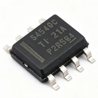
BQ24133RGYR - 2.5A 1.6MHz Sync Buck Charger | TI
Référence : BQ24133RGYR ✓ Actif| Qté | Prix unitaire | Total |
|---|---|---|
| 1 | $2.35 | $2,35 |
| 10 | $2.11 | $21,10 |
| 100 | $1.9 | $190,00 |
| 500 | $1.78 | $890,00 |
| 1 000 | $1.69 | $1 690,00 |
BQ24133RGYR Présentation
A battery charger IC is a power-management device that safely controls charging current and voltage for rechargeable cells. The BQ24133 uses a synchronous buck converter topology to step down input voltage efficiently, minimizing heat compared to linear chargers. It belongs to the battery management IC hierarchy within power management semiconductors, essential for portable electronics, tools, and medical devices.
Key features include high-accuracy regulation with plus/minus 1% charge voltage accuracy, a wide input range from a DC source as high as 17V including automotive car batteries, and an adjustable input overvoltage limit via the OVPSET pin with 30V rating on AVCC, ACP, and ACN pins. An integrated power path selector lets the system run from the adapter while charging the battery, and an external thermistor enables charging only within a safe temperature window.
Technically, the constant-frequency synchronous PWM controller at 1.6 MHz permits small inductors and capacitors. Charge current is programmable via an external resistor, and cell count is configured for 1, 2, or 3 series cells. Thermal regulation reduces charge current when die temperature exceeds threshold, and a low-power sleep mode minimizes battery drain when input is removed. On high-voltage DC insertion, Q1 and Q2 remain off to protect the system.
Typical applications include smartphones, tablets, digital cameras, power banks, solar-powered chargers, battery-powered industrial equipment, and medical devices.
Design tip: ensure adequate copper pour for thermal dissipation and place input/output capacitors close to the IC; select the inductor based on the 1.6-MHz switching frequency to minimize ripple.
Alternatives de remplacement direct pour BQ24133RGYR — même boîtier, compatible broche à broche. Les références à boîtier différent nécessitant une retouche du PCB sont exclues.
Variantes de cette série
Modèles de la même série directement compatibles avec BQ24133RGYR (même facteur de forme et même empreinte) — différant par Battery Temperature Monitoring, Cell Count.
Outil de comparaison rapide — sélectionnez des références alternatives pour une comparaison côte à côte :
BQ24133QRGYR
✅ Remplacement direct✓ En stock
$2.53 / unité
Voir la fiche technique →BQ24130RGYR
⚡ Même boîtier ⚠️ Spécifications non vérifiées📋 Alternative de référence (hors catalogue)
BQ24133RGYR Spécifications
| Battery Chemistry | Li-Ion / Li-Polymer |
| Cell Count | 1, 2, or 3 series cells |
| Maximum Charge Current | 2.5 A |
| Charger Topology | Synchronous buck (switch-mode) |
| Fréquence de commutation | 1.6 MHz |
| Input Voltage (DC source) | Up to 17 V (car battery compatible) |
| Pin Voltage Rating (AVCC/ACP/ACN) | 30 V |
| Charge Voltage Accuracy | ±1% |
| Integrated MOSFETs | Two N-channel power MOSFETs |
| Power Path Management | Yes (external power path selector) |
| Input OVP | Adjustable via OVPSET pin |
| Battery Temperature Monitoring | External thermistor (TS pin) |
| Thermal Regulation | Charge current reduction at high die temperature |
| Température de fonctionnement | -40°C to +85°C |
| Boîtier | VQFN-24 (RGY) 5.5 x 3.5 mm |
| Type de montage | Surface Mount |
| Niveau MSL | 2 (260°C, 1 year) |
| Sleep Mode | Yes (low-power when input removed) |
Configuration des broches de BQ24133RGYR
| Broche 1 | AVCC — Analog input supply, 30V rated |
| Broche 4 | ACP — Adapter/input power sense node, 30V rated |
| Broche 5 | ACN — Input current sense node, 30V rated |
| Broche 6 | OVPSET — Adjustable input overvoltage limit setpoint |
| Broche 10 | ISET — Charge current programming (external resistor) |
| Broche 12 | TS — Battery temperature thermistor input |
| Broche 13 | VFB / CELL — Voltage feedback / cell count select (1-3 cells) |
| Broche 20 | PH — Switching node between integrated MOSFETs |
| Broche 24 | PGND — Power ground |
| Broche 17 | BTST / BOOT — High-side MOSFET driver bootstrap |
Applications typiques
BQ24133RGYR convient pour 6 applications: Smartphones and Tablets, Power Banks, Automotive and 12V Bus Charging, Solar-Powered Chargers, Medical and Portable Instruments, Industrial Handheld Equipment.
Smartphones and Tablets
The BQ24133's 2.5A charge current and 1.6-MHz switching frequency enable rapid charging with small external inductors and capacitors, ideal for thin portable devices. The integrated power path selector lets the phone run from the adapter while charging, supporting instant power-on with a deeply discharged battery. Thermal regulation prevents overheating in enclosed enclosures. Sourced from TI datasheet Rev. D typical applications.
Recommandé
Power Banks
Power banks benefit from the BQ24133's synchronous buck efficiency and integrated MOSFETs, which reduce BOM count and board area. The 1-3 cell configuration covers common 1S and 2S/3S pack architectures, while the external thermistor on TS pin enables safe charging of Li-Polymer pouch cells. The 17V maximum input allows charging from 12V adapters as well as 5V sources.
Recommandé
Automotive and 12V Bus Charging
With a DC input as high as 17V including car batteries and 30V transient rating on AVCC, ACP, and ACN pins, the BQ24133 survives automotive load-dump-adjacent conditions. The OVPSET pin adjusts the input overvoltage limit to match 12V vehicle bus ranges. The Q1 variant (BQ24133QRGYRQ1) provides AEC-Q100 qualification for production automotive designs.
Recommandé
Solar-Powered Chargers
The BQ24133's 17V input limit and adjustable input OVP via OVPSET accommodate typical 12V solar panels. The stand-alone operation requires no host microcontroller, reducing firmware complexity in solar garden lights and remote sensors. Designers should verify panel IV characteristics since the part lacks dedicated MPPT; adding input current limiting through the OVPSET network helps avoid panel collapse.
Recommandé
Medical and Portable Instruments
Battery-powered medical devices require accurate and safe charging. The BQ24133's ±1% charge voltage accuracy maximizes capacity use without overcharging cells, and the thermistor window prevents charging outside safe temperatures - a key patient-safety requirement. The low-power sleep mode minimizes battery drain when the charger input is removed, extending shelf life of portable diagnostic instruments.
Recommandé
Industrial Handheld Equipment
Two-way radios, barcode scanners, and test tools charge from 12V industrial adapters through the BQ24133's wide input range. The 30V pin rating on the ACN/ACP pins adds robustness against adapter hot-plug transients, and the power path selector keeps the device operational during charging - critical for duty-cycle equipment. Thermal regulation protects against high-ambient dock charging conditions.
Recommandé
Récapitulatif des produits recommandés
Données de référence d'ingénierie pour BQ24133RGYR — comparaison, recommandations de conception et informations de conformité.
Guide de sélection
Comparaison avec les alternatives
| Paramètre | Ce produit | BQ24133QRGYRQ1 | BQ24130RGYR |
|---|---|---|---|
| Package | VQFN-24 (RGY) 5.5x3.5 mm | VQFN-24 (RGY) - same | VQFN-24 (RGY) - same |
| Brand | Texas Instruments | Texas Instruments | Texas Instruments |
| Max Charge Current | 2.5 A | 2.5 A | 2.5 A |
| Cell Count | 1-3 cells | 1-3 cells | 1-3 cells |
| Switching Frequency | 1.6 MHz | 1.6 MHz | 1.6 MHz |
| Grade | Commercial/Industrial | AEC-Q100 (Q1) | Commercial |
| Power Path Selector | Yes | Yes | Yes |
Principaux différenciateurs
- Standard grade at lower cost (vs BQ24133QRGYRQ1)
- Stand-alone operation with integrated MOSFETs (vs BQ24610QRGERQ1)
- 1.6 MHz switching frequency (vs BQ24130RGYR)
Notes de conception
At 2.5A charge current with a large VIN-VOUT delta, the integrated MOSFETs dissipate significant power. Use the VQFN-24 exposed thermal pad with a solid ground plane and at least 4-6 thermal vias to inner layers. The BQ24133's thermal regulation feature will reduce charge current if the die overheats, which extends charge time - good copper design prevents this in enclosed products.
At 1.6 MHz switching frequency, keep the power loop (ACP - ACN - PH - inductor - battery) as short and tight as possible. Place input ceramic capacitors within 2-3 mm of AVCC/ACP pins and output capacitors at the battery node. Follow the PCB layout example in TI datasheet Rev. D, section on application information.
Size the inductor for the 1.6-MHz frequency with adequate saturation current above the 2.5A charge current plus ripple. Set OVPSET correctly for the input source: too low a threshold causes nuisance shutdowns with long adapter cables. Use 1% tolerance resistors for voltage feedback to preserve the ±1% charge voltage accuracy. Do not omit the TS thermistor network - charging outside the safe window risks cell damage.
Informations de conformité
MSL Level 2 (260°C, 1 year) per PartGenie. AEC-Q100 qualification applies to the BQ24133QRGYRQ1 variant, not the standard BQ24133RGYR. Confirm RoHS/REACH status on TI product page.