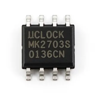
ICS511MIT - 160MHz PLL Clock Multiplier | Renesas | 8-SOIC
Référence : ICS511MIT ✗ Fin de vieICS511MIT Présentation
A PLL clock multiplier belongs to the clock and timing IC family. Unlike a simple logic inverter or buffer, it uses a phase-locked loop to lock an internal or output frequency to a stable reference and multiply that reference by an integer ratio. Clock generators and frequency synthesizers sit within the broader timing-control hierarchy used to coordinate processors, transceivers, memory, and data-conversion equipment.
The primary identified characteristics are a 160 MHz maximum clock frequency, a PLL clock-multiplier function, and an 8-SOIC package measuring 0.154 inch, or 3.90 mm, in body width. The ICS511MIT is also described as a high-frequency clock generator intended for precision applications. Its supported input sources are identified as a clock or crystal, and it belongs to the ICS511 series.
Because the device is obsolete, lifecycle planning is more important than headline performance differences. An existing design can often continue using the same ICS511 family pin arrangement, but a clock source is a board-level dependency: replacement parts must reproduce the reference frequency, output frequency range, output drive, and pin mapping. A nominal maximum frequency alone does not guarantee timing compatibility with an existing circuit.
Typical uses include precision frequency multiplication in communications equipment, clock distribution for high-speed digital subsystems, test and measurement instrumentation, and timing architectures that require a derived clock rather than a free-running oscillator. In such systems, the PLL output replaces or supplements a lower-frequency reference while preserving phase coherence with the reference source.
When laying out a board, route the reference input and clock outputs away from noisy switching nodes and provide a stable ground reference beneath the device. Keep clock traces short, use controlled-impedance routing when operating at high edge rates, and confirm the exact output-divider and feedback configuration against the manufacturer datasheet before releasing a new layout.
This page combines the identified device characteristics, lifecycle information, cross-reference results, and practical clock-tree guidance. It also documents the limitations of an obsolete timing IC so procurement and engineering teams can assess redesign risk rather than relying on a headline frequency rating alone.
Alternatives de remplacement direct pour ICS511MIT — même boîtier, compatible broche à broche. Les références à boîtier différent nécessitant une retouche du PCB sont exclues.
Variantes de cette série
Modèles de la même série directement compatibles avec ICS511MIT (même facteur de forme et même empreinte) — différant par Package, Product Type, Manufacturer, Series.
ICS511M
✅ Remplacement directContactez-nous pour le prix
Voir la fiche technique →ICS511MT
✅ Remplacement directContactez-nous pour le prix
Voir la fiche technique →ICS511MI
✅ Remplacement directContactez-nous pour le prix
Voir la fiche technique →ICS511ML
✅ Remplacement direct ⚠️ Spécifications non vérifiées📋 Alternative de référence (hors catalogue)
ICS511MIT Spécifications
| Product Type | PLL clock multiplier / clock generator IC |
| Manufacturer | Renesas Electronics |
| Series | ICS511 |
| Fréquence d'horloge maximale | 160 MHz |
| Multiplier Output | 1 |
| Reference Input | Clock or crystal |
| PLL | Yes |
| Boîtier | 8-SOIC |
| Package Body Width | 0.154 inch (3.90 mm) |
| Type de montage | Surface mount |
| Shipping Format | Tape and reel |
| Product Status | Obsolete |
| Programmability | Not verified |
Guide de configuration des broches du ICS511MIT 0.154 inch (3.90 mm)
Configuration des broches du ICS511MIT (boîtier 0.154 inch (3.90 mm)). La numérotation des broches, les fonctions et les schémas de connexion sont définis dans la fiche technique du fabricant. Consultez-la pour l'empreinte exacte et les directives de soudage.

Aucune donnée de brochage détaillée disponible pour ICS511MIT.
Consultez la fiche technique pour la configuration complète des broches.
Applications typiques
ICS511MIT convient pour 6 applications: Precision Communications Clocking, High-Speed Digital Subsystem Clocking, Test and Measurement Instrumentation, Industrial Control and Data Acquisition, Phase-Coherent Clock Distribution, Legacy System Maintenance and Repair.
Precision Communications Clocking
The ICS511MIT is suitable for a communications subsystem that needs a higher-frequency, phase-coherent clock derived from a lower-frequency reference. Its PLL clock-multiplier architecture and listed 160 MHz maximum frequency make it appropriate for serializer, transceiver, or high-speed digital interface timing. Place the reference source close to the device, keep the feedback and output routes short, and confirm that the required multiplication ratio and output frequency fall within the part-specific limits in the datasheet. Because the ICS511MIT is obsolete, it is most appropriate for maintaining an existing qualified design rather than driving a new platform.
Recommandé
High-Speed Digital Subsystem Clocking
Use the ICS511MIT to create a multiplied clock for logic that requires more clock frequency than the board reference can supply directly. The identified 160 MHz capability supports high-speed clock-tree sections in processor, storage, and data-conversion systems, provided the actual output range and output-drive requirements are verified from the manufacturer datasheet. Route the clock as a transmission-line class net if rise time demands it, avoid unnecessary stubs, and keep switching regulators and high-current nets physically separated from the reference and clock outputs.
Recommandé
Test and Measurement Instrumentation
The ICS511MIT can supply a derived clock for instrumentation requiring a stable reference relationship across multiple internal circuits. Using a PLL multiplier allows a single crystal-derived reference to support other clock domains while maintaining a defined relationship to the source. The design must account for reference purity, output jitter, and the propagation delay through the feedback loop. Validate the maximum frequency and reference-input conditions in the datasheet, and measure the generated clock at the load rather than relying only on an unloaded probe point.
Recommandé
Industrial Control and Data Acquisition
The ICS511MIT can support industrial control and data-acquisition boards that synchronize sampling, conversion, and processing sections to a common reference. Its listed clock-generator function, PLL capability, and 160 MHz maximum frequency suit systems requiring deterministic timing relationships between modules. Keep analog and power-conversion sections separated from the clock generator, maintain a low-impedance ground return, and verify the operating-temperature grade before using the part in industrial equipment. For new platforms, evaluate the current supported alternative alongside the legacy ICS511 family.
Recommandé
Phase-Coherent Clock Distribution
Use the ICS511MIT when several logic domains must remain phase-coherent rather than simply receive independent oscillator outputs. A PLL-multiplied clock provides a derived frequency with a defined relationship to its clock or crystal reference, which is useful for parallel data paths, converters, and timing controllers. The reference trace should be short and isolated, while clock outputs should be buffered or routed according to the load capacitance specified by the manufacturer. Scope the waveform at the far end of the board to verify amplitude, edge quality, and absence of reflected pulses.
Recommandé
Legacy System Maintenance and Repair
The ICS511MIT is most relevant to maintenance, repair, and lifecycle-extension programs for equipment that already uses the ICS511 family. Its 8-SOIC package and identified 160 MHz clock-generator specification support controlled substitution within an existing design, provided the reference-input range, pin mapping, supply requirements, and temperature grade are confirmed. Document any alternate ordering code in the equipment records and perform timing measurements after replacement. New production quantities should be reserved for spares rather than assumed as a guaranteed long-term supply.
Recommandé
Récapitulatif des produits recommandés
Données de référence d'ingénierie pour ICS511MIT — comparaison, recommandations de conception et informations de conformité.
Guide de sélection
Comparaison avec les alternatives
| Paramètre | Ce produit | ICS511M | ICS511MT | ICS511MI | ICS511ML |
|---|---|---|---|---|---|
| Package | 8-SOIC | 8-SOIC | 8-SOIC | 8-SOIC | 8-SOIC |
| Brand | Renesas Electronics | Renesas Electronics | Renesas Electronics | Renesas Electronics | Renesas Electronics |
Principaux différenciateurs
- Documented high-frequency ICS511 clock-generator positioning (vs ICS511M)
- Same-family alternative with matching tape-and-reel logistics (vs ICS511MI)
- Direct ordering-code continuity within the ICS511 family (vs ICS511MT)
Notes de conception
Treat the reference input and clock outputs as high-speed signals even when the reference frequency is relatively low. Place the ICS511MIT close to the oscillator or crystal network, keep the reference path short, and avoid routing it beneath digital return currents. Place any crystal at the device pins and keep unrelated high-current switching nodes away from the oscillator area to reduce supply-to-output coupling and clock jitter.
Confirm output amplitude, edge rate, and load capability at the far end of the clock route. If the trace length or edge rate creates a transmission-line condition, use a controlled-impedance layout with a defined termination strategy instead of relying on a point probe at the generator. Avoid long stubs and test taps that add capacitive loading, because either effect can degrade rise time and shift the timing relationship seen by downstream logic.
Do not treat every ICS511 ordering code as electrically identical. Verify the exact pinout, supply voltage, reference-frequency range, output-frequency limit, temperature grade, and feedback configuration before replacing the ICS511MIT. A package match and a 160 MHz class headline value do not prove timing compatibility. For production maintenance, record the approved alternate part number and validate it against the original schematic and operating envelope.
Follow the manufacturer bypass-capacitor recommendations and provide the required supply decoupling directly at the device pins. A clock generator can translate supply noise directly into output jitter, especially when the PLL multiplies a reference containing periodic disturbances. Route the return current through an uninterrupted ground plane, keep the decoupling loop compact, and verify supply ripple at the IC rather than only at the power supply connector.
Informations de conformité
The indexed product information identifies the device as obsolete but does not state RoHS, REACH, AEC-Q100, lead-free, halogen-free, or conflict-minerals status. Compliance attributes therefore remain unknown.