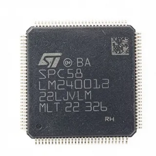
LPC4323JBD144E - Dual-Core Cortex-M4/M0 MCU | NXP
Référence : LPC4323JBD144E ✓ ActifLPC4323JBD144E Présentation
A microcontroller is a programmable semiconductor platform that combines a processor core, memory, communication peripherals, timers, and I/O in one integrated circuit. The LPC4323JBD144E belongs to the Arm Cortex-M4 microcontroller family and sits within the broader embedded-processing and power-management hierarchy. Its two-core architecture can divide control, communications, and real-time work between Cortex-M4 and Cortex-M0 domains while retaining a unified software-development environment.
The LPC4323 part family supports Arm Cortex-M4 processing with an Arm Cortex-M0 coprocessor capable of operation up to 204 MHz. The supplied product information identifies 512 kB flash and 136 kB SRAM for LPC4323JBD144, two high-speed USB ports, Ethernet connectivity, and LCD support. A quad SPI Flash Interface, State Configurable Timer, Serial General Purpose I/O interface, and EEPROM memory are also identified as family-level features.
The LQFP-144 package provides 144 external leads and supports access to the device's extensive communications and general-purpose I/O resources. Because the target is a pin-intensive mixed-signal microcontroller rather than a simple power component, careful assignment of pins is necessary when designing PCB fanout, USB, Ethernet, display, and external-memory interfaces. The package is supplied in tray packaging according to the verified distributor listing.
Typical uses include industrial Ethernet equipment, USB-to-serial or protocol-conversion controllers, human-machine interface controllers, connected test equipment, and embedded gateways. The Ethernet and dual high-speed USB resources make the device suitable for systems that must bridge multiple communication standards while using the Cortex-M0 core for background control or low-power peripheral servicing.
The principal design consideration is firmware and board planning rather than a simple power-rail trade-off. Designers should reserve the required USB, Ethernet, LCD, clock, reset, debug, and programming pins before assigning general-purpose I/O. The exact pin names, multiplexing limits, clock requirements, decoupling values, and analog characteristics should be checked against the manufacturer datasheet before schematic capture.
This page consolidates the verified manufacturer and distributor information for the LPC4323JBD144E, identifies same-family LQFP-144 alternatives, and separates confirmed specifications from parameters that still require datasheet verification. That distinction helps engineers compare procurement options without mistaking a family relationship for complete application-level equivalence.
Alternatives de remplacement direct pour LPC4323JBD144E — même boîtier, compatible broche à broche. Les références à boîtier différent nécessitant une retouche du PCB sont exclues.
Variantes de cette série
Modèles de la même série directement compatibles avec LPC4323JBD144E (même facteur de forme et même empreinte) — différant par Flash Memory, Package.
LPC4323JBD144
✅ Remplacement direct ⚠️ Spécifications non vérifiées📋 Alternative de référence (hors catalogue)
LPC4322JBD144
✅ Remplacement direct ⚠️ Spécifications non vérifiées📋 Alternative de référence (hors catalogue)
LPC4321JBD144
✅ Remplacement direct ⚠️ Spécifications non vérifiées📋 Alternative de référence (hors catalogue)
LPC4325JBD144E
✅ Remplacement direct ⚠️ Spécifications non vérifiéesContactez-nous pour le prix
Voir la fiche technique →LPC4353JBD144
✅ Remplacement direct ⚠️ Spécifications non vérifiées📋 Alternative de référence (hors catalogue)
LPC4323JBD144E Valeurs maximales et caractéristiques électriques
| Product Type | 32-bit dual-core microcontroller (MCU) |
| Primary Processor Core | Arm Cortex-M4 |
| Coprocessor Core | Arm Cortex-M0 |
| Cortex-M0 Coprocessor Maximum Frequency | 204 MHz |
| Flash Memory | 512 kB |
| On-Chip SRAM | 136 kB |
| Family Maximum Flash Memory | Up to 1 MB |
| Family EEPROM Memory | Up to 16 kB |
| High-Speed USB Interfaces | 2 |
| Ethernet Support | Yes |
| LCD Support | Yes |
| Quad SPI Flash Interface | Yes |
| State Configurable Timer | Yes |
| Serial General Purpose I/O Interface | Yes |
| Tension d'alimentation | 3.3 V |
| Boîtier | LQFP-144 |
| Type de montage | Surface Mount |
| Manufacturer Product Family | LPC435x/3x/2x/1x |
Guide de configuration des broches du LPC4323JBD144E lqfp-144
Configuration des broches du LPC4323JBD144E (boîtier lqfp-144). Ce circuit intégré numérique comprend des GPIO, des interfaces de communication (UART, SPI, I2C) et des broches d'alimentation. Consultez la fiche technique du fabricant pour les fonctions alternatives des broches et les options de configuration. Indispensable pour la conception de systèmes embarqués et la conception de circuits imprimés.
Aucune donnée de brochage détaillée disponible pour LPC4323JBD144E.
Consultez la fiche technique pour la configuration complète des broches.
Applications typiques
LPC4323JBD144E convient pour 6 applications: Industrial Ethernet Gateway Controller, USB Protocol Converter, Human-Machine Interface Controller, Connected Test and Measurement Instrument, Embedded Data Acquisition Controller, Embedded Communications Coprocessor.
Industrial Ethernet Gateway Controller
The LPC4323JBD144E fits an industrial Ethernet gateway because it combines an Arm Cortex-M4 processor, an Arm Cortex-M0 coprocessor, 512 kB flash, 136 kB SRAM, and verified Ethernet support in an LQFP-144 package. The Cortex-M4 can handle protocol processing and gateway logic, while the Cortex-M0 can service control tasks or peripheral interrupts independently. Its two high-speed USB interfaces add a path for local configuration, diagnostics, or storage. Compared with a single-core MCU, the architecture allows workload partitioning without adding a second package. The implementation still requires verified Ethernet PHY integration, isolation requirements, controlled-impedance routing, clock planning, and exact NXP pin-multiplexing checks before the board is released.
Recommandé
USB Protocol Converter
The LPC4323JBD144E is appropriate for a USB-to-serial or USB-to-fieldbus converter because it provides two high-speed USB interfaces, 512 kB flash, and 136 kB SRAM for protocol stacks and buffering. One USB port can serve as the host-facing interface while another supports a peripheral function, subject to the device's verified USB role and pin assignments. The Cortex-M0 coprocessor can support lightweight status monitoring while the Cortex-M4 executes USB and protocol software. In a production design, USB connector routing, differential-pair geometry, common-mode filtering, power requirements, and firmware support for the selected USB class are the main engineering constraints. The supplied data does not quantify USB data rates, so the current NXP datasheet must be checked before bandwidth commitments are made.
Recommandé
Human-Machine Interface Controller
The LPC4323JBD144E can serve as the central controller in an embedded human-machine interface because the verified LPC4323 product information identifies LCD support alongside Ethernet and dual high-speed USB. Its 512 kB flash accommodates graphical firmware, fonts, and interface assets, while 136 kB SRAM supports working memory and display buffers. The Cortex-M4 core can run the primary interface and communications logic, and the Cortex-M0 coprocessor can handle periodic input scanning or status updates. Engineering attention should focus on the selected LCD interface, panel-specific timing, backlight control, touch-controller connectivity, and the exact I/O mux assigned to the display. Since no LCD resolution or controller timing is provided in the verified data, those values must be established from the manufacturer datasheet and selected display module documentation.
Recommandé
Connected Test and Measurement Instrument
The LPC4323JBD144E fits connected instrumentation that needs flexible processing, multiple communication paths, and substantial SRAM. The Arm Cortex-M4 core can execute acquisition control and user-interface logic, the Cortex-M0 coprocessor can handle background peripheral tasks, and the verified 136 kB SRAM provides working memory for local buffering. Ethernet supports host connectivity, while the two high-speed USB interfaces can serve as a control link or peripheral connection. The LQFP-144 package offers many external signals for front-panel controls, displays, and instrument buses. Signal integrity, analog isolation, grounding, and USB or Ethernet implementation remain system-level responsibilities; the supplied snippets do not specify converter accuracy or acquisition-channel performance, so analog front-end design must be handled separately from the MCU selection.
Recommandé
Embedded Data Acquisition Controller
The LPC4323JBD144E is suitable for a data-acquisition controller that must combine real-time control with buffered communications. The Cortex-M4 core provides the primary execution environment for sequencing and data handling, while the Cortex-M0 coprocessor can execute a simpler control loop or service timing-critical peripherals. The confirmed 512 kB flash stores firmware and configuration, and 136 kB SRAM provides a local working buffer for short acquisition segments. Ethernet and two high-speed USB interfaces allow the controller to transfer results to a host or storage peripheral. The primary design caveat is that the verified data does not define ADC channels, conversion speed, DAC performance, or pin multiplexing for a specific sensor interface. Those parameters must be matched to the chosen external converter and NXP pin assignment before architecture approval.
Recommandé
Embedded Communications Coprocessor
The LPC4323JBD144E can act as a dedicated communications processor in a larger embedded system because its dual-core architecture provides a Cortex-M4/M0 split within one package. The Cortex-M4 can execute protocol conversion, packet processing, and USB or Ethernet tasks, while the Cortex-M0 coprocessor performs low-complexity monitoring, control, or peripheral servicing. The verified 512 kB flash and 136 kB SRAM provide resources for firmware and working data, and the LQFP-144 package exposes the wide set of family peripherals. The trade-off is that software partitioning must be planned explicitly because both cores share device-level resources. Interrupt ownership, memory arbitration, boot behavior, clock configuration, and peripheral pin allocation are not detailed in the supplied snippets and must be confirmed from the current NXP technical documentation before splitting workloads across the cores.
Recommandé
Récapitulatif des produits recommandés
Données de référence d'ingénierie pour LPC4323JBD144E — comparaison, recommandations de conception et informations de conformité.
Guide de sélection
Comparaison avec les alternatives
| Paramètre | Ce produit | LPC4323JBD144 | LPC4322JBD144 | LPC4321JBD144 | LPC4325JBD144 | LPC4353JBD144 |
|---|---|---|---|---|---|---|
| Brand | NXP Semiconductors | NXP Semiconductors | NXP Semiconductors | NXP Semiconductors | NXP Semiconductors | NXP Semiconductors |
| Package | LQFP-144 | LQFP-144 | LQFP-144 | LQFP-144 | LQFP-144 | LQFP-144 |
| Processor Architecture | Arm Cortex-M4/M0 | Arm Cortex-M4/M0 | Arm Cortex-M4/M0 family | Arm Cortex-M4/M0 family | Arm Cortex-M4/M0 family | Arm Cortex-M4/M0 family |
| Special Feature | Arm Cortex-M0 coprocessor | Arm Cortex-M0 coprocessor | Arm Cortex-M0 coprocessor | Arm Cortex-M0 coprocessor | Arm Cortex-M0 coprocessor | Arm Cortex-M0 coprocessor |
Principaux différenciateurs
- Confirmed 512 kB flash configuration (vs LPC4353JBD144)
- Verified 136 kB SRAM for the specified LPC4323 device (vs LPC4321JBD144)
- Confirmed dual high-speed USB interfaces (vs LPC4322JBD144)
- Confirmed Ethernet and LCD integration (vs LPC4323JBD144)
Notes de conception
Reserve the NXP-recommended USB and Ethernet pins before assigning general-purpose I/O, and route USB differential pairs as controlled-impedance nets over a continuous reference plane. Place any Ethernet magnetics or PHY close to the corresponding connector, while keeping high-current and switching-regulator paths away from sensitive communications. The supplied data confirms USB, Ethernet, and LCD functions but does not provide routing dimensions, so the final layout must follow the current NXP hardware-design guidance and selected PHY or transceiver reference design.
Use the manufacturer's recommended supply topology, decoupling values, and power-up sequence rather than a generic 3.3 V regulator arrangement. The verified listing confirms a 3.3 V device but does not specify total current, internal core-voltage requirements, or bypass capacitance. Place each required capacitor adjacent to its corresponding power pin, provide low-impedance supply and ground planes, and verify startup behavior across the complete temperature and voltage range. Unsupported power values must be obtained from the current datasheet before schematic release.
Do not treat all LQFP-144 LPC43xx devices as automatically interchangeable merely because they use the same package. Confirm flash size, SRAM availability, Ethernet MAC or PHY requirements, USB roles, LCD resources, clock configuration, and every multiplexed pin. Also verify the meaning of the E ordering suffix against the NXP ordering table. A board-level migration is acceptable only after compiling the target and replacement pin functions and confirming startup, debug, and firmware dependencies.
Treat the 144-pin package as a pin-constrained design rather than a generic surface-mount part. Build the pin assignment around dedicated power, reset, clock, debug, USB, Ethernet, LCD, and programming functions first, then assign multiplexed signals. Check the package pin numbering in the manufacturer datasheet and the selected LQFP-144 land pattern. Maintain adequate assembly clearances, thermal-via strategy, and ground return paths around the fine-pitch leads to reduce soldering and EMC risk.
Informations de conformité
The supplied web results do not explicitly state the component's RoHS, REACH, AEC-Q100, lead-free, halogen-free, or conflict-minerals status. These values remain unknown rather than being inferred from the manufacturer or package.