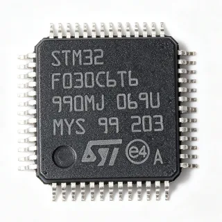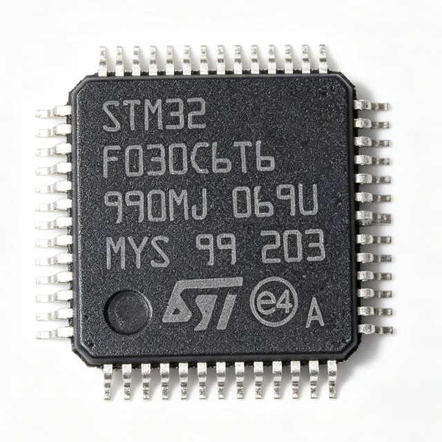
STM32F030C6T6 - 48MHz Cortex-M0 MCU, 32KB Flash, LQFP-48 | STMicroelectronics
Référence : STM32F030C6T6 ✓ Actif| Qté | Prix unitaire | Total |
|---|---|---|
| 1 | $2.45 | $2,45 |
| 10 | $2.12 | $21,20 |
| 100 | $1.78 | $178,00 |
| 500 | $1.42 | $710,00 |
| 1 000 | $1.15 | $1 150,00 |
STM32F030C6T6 Présentation
What is a microcontroller? A microcontroller (MCU) is a compact integrated circuit that combines a processor core, non-volatile program memory (Flash), volatile data memory (SRAM), and programmable input/output peripherals on a single die. In the system hierarchy, an MCU is an embedded processor, which falls under the broader category of integrated circuits and semiconductors. The STM32F030C6T6 sits in the mainstream 32-bit segment, positioned above legacy 8-bit MCUs and below high-performance application processors, offering an economical entry point into the ARM Cortex-M ecosystem with deterministic real-time behavior.
Key features of the STM32F030C6T6 include a 12-bit SAR ADC with up to 10 external channels, two 16-bit general-purpose timers plus one 16-bit advanced-control timer for PWM, a 32-bit real-time timer, and a 5-channel DMA controller. Communication interfaces comprise I2C, SPI, and USART, and the device exposes up to 39 GPIO pins. The integrated 4 MHz to 32 MHz external crystal oscillator and internal 8 MHz RC with PLL enable flexible clocking. Low-power Sleep, Stop, and Standby modes are supported for battery-powered designs.
From a technical perspective, the Cortex-M0 core implements the ARMv6-M architecture with a 3-stage pipeline, delivering 0.9 DMIPS/MHz and supporting Thumb/Thumb-2 instruction subsets. The 32 KB Flash supports read-while-write, enabling in-field firmware upgrades without halting execution. A 96-bit unique device ID and a cyclic redundancy check (CRC) hardware unit assist in traceability and data integrity. The NVIC provides deterministic interrupt handling with configurable priority levels.
Typical applications include industrial sensor interfaces, home automation nodes, consumer white goods, low-cost motor control, LED lighting drivers, and USB-to-UART bridges. The combination of timers, ADC, and DMA enables efficient closed-loop control, while the small LQFP-48 footprint supports compact PCB layouts.
When designing with this device, decouple each VDD pin with a 100 nF X7R ceramic capacitor placed within 3 mm of the pin, and add a 4.7 uF bulk capacitor on the main rail. Configure the BOOT0 pin to select Flash, System memory (USART bootloader), or SRAM boot. The SWD interface requires only two pins (SWDIO/SWCLK) plus GND, simplifying in-circuit programming and debug.
This page synthesizes distributor pricing, drop-in alternatives, and practical design notes not found in the ST datasheet, providing a comprehensive resource for engineers evaluating the STM32F030C6T6.
Alternatives de remplacement direct pour STM32F030C6T6 — même boîtier, compatible broche à broche. Les références à boîtier différent nécessitant une retouche du PCB sont exclues.
Variantes de cette série
Modèles de la même série directement compatibles avec STM32F030C6T6 (même facteur de forme et même empreinte) — différant par Package, Communication Interfaces, Core, Flash Memory, Timers.
Outil de comparaison rapide — sélectionnez des références alternatives pour une comparaison côte à côte :
STM32F030C8T6
✅ Remplacement direct✓ En stock
$0.98 / unité
Voir la fiche technique →STM32F030CCT6
✅ Remplacement direct✓ En stock
$1.48 / unité
Voir la fiche technique →STM32F030F4P6
✅ Remplacement direct✓ En stock
$0.5768 / unité
Voir la fiche technique →HK32F030C6T6
✅ Remplacement direct📋 Alternative de référence (hors catalogue)
STM32F030C6T6 Valeurs maximales et caractéristiques électriques
| Core Architecture | ARM Cortex-M0 32-bit RISC |
| Fréquence d'horloge maximale | 48 MHz |
| Flash Memory | 32 KB |
| SRAM | 4 KB |
| Supply Voltage Range | 2.4 V to 3.6 V |
| Température de fonctionnement | -40 C to +85 C |
| Boîtier | 48-pin LQFP (7x7 mm) |
| ADC | 12-bit SAR, up to 10 channels |
| Timers | 1x 16-bit advanced-control, 2x 16-bit general-purpose, 1x 32-bit RTC |
| DMA Channels | 5 |
| Communication Interfaces | 1x I2C, 1x SPI, 1x USART |
| GPIO Count | 39 |
| Debug Interface | Serial Wire Debug (SWD), 2-pin |
| Low-Power Modes | Sleep, Stop, Standby |
| Statut RoHS | Compliant |
| Niveau MSL | 3 |
Configuration des broches de STM32F030C6T6
| Broche 1 | PB8 — General-purpose I/O / I2C1 SCL (alternate function) |
| Broche 2 | BOOT0 — Boot mode selection (Flash / System memory / SRAM) |
| Broche 3 | PB9 — General-purpose I/O / I2C1 SDA (alternate function) |
| Broche 4 | NRST — Reset input, active low; internal pull-up |
| Broche 5 | VDDA — Analog supply voltage (2.4 V to 3.6 V) |
| Broche 6 | PA0 — GPIO / ADC_IN0 / WKUP / TIM2_CH1 |
| Broche 7 | PA1 — GPIO / ADC_IN1 / TIM2_CH2 |
| Broche 8 | PA2 — GPIO / ADC_IN2 / USART1_TX / TIM15_CH1 |
| Broche 9 | PA3 — GPIO / ADC_IN3 / USART1_RX / TIM15_CH2 |
| Broche 10 | PA4 — GPIO / ADC_IN4 / SPI1_NSS / TIM14_CH1 |
| Broche 11 | PA5 — GPIO / ADC_IN5 / SPI1_SCK / TIM2_CH1_ETR |
| Broche 12 | PA6 — GPIO / ADC_IN6 / SPI1_MISO / TIM3_CH1 / TIM16_CH1 |
| Broche 13 | PA7 — GPIO / ADC_IN7 / SPI1_MOSI / TIM3_CH2 / TIM17_CH1 |
| Broche 14 | PB0 — GPIO / ADC_IN8 / TIM3_CH3 |
| Broche 15 | PB1 — GPIO / ADC_IN9 / TIM3_CH4 |
| Broche 16 | PB2 — GPIO / BOOT1 (alternate function) |
| Broche 17 | VDD — Digital supply voltage (2.4 V to 3.6 V) |
| Broche 18 | VSS — Digital ground |
| Broche 19 | PA8 — GPIO / USART1_CK / TIM1_CH1 / MCO |
| Broche 20 | PA9 — GPIO / USART1_TX / TIM1_CH2 / I2C1_SCL |
| Broche 21 | PA10 — GPIO / USART1_RX / TIM1_CH3 / I2C1_SDA |
| Broche 22 | PA11 — GPIO / USART1_CTS / TIM1_CH4 |
| Broche 23 | PA12 — GPIO / USART1_RTS / TIM1_ETR |
| Broche 24 | PA13 — GPIO / SWDIO (debug) |
| Broche 25 | VSS — Digital ground |
| Broche 26 | VDD — Digital supply voltage (2.4 V to 3.6 V) |
| Broche 27 | PA14 — GPIO / SWCLK (debug) |
| Broche 28 | PA15 — GPIO / SPI1_NSS / TIM2_CH1_ETR |
| Broche 29 | PB3 — GPIO / SPI1_SCK / TIM2_CH2 |
| Broche 30 | PB4 — GPIO / SPI1_MISO / TIM3_CH1 |
| Broche 31 | PB5 — GPIO / SPI1_MOSI / TIM3_CH2 |
| Broche 32 | PB6 — GPIO / USART1_TX / I2C1_SCL / TIM16_CH1_N |
| Broche 33 | PB7 — GPIO / USART1_RX / I2C1_SDA / TIM17_CH1_N |
| Broche 34 | BOOT0 — Boot mode selection (shared with PB8 via option byte) |
| Broche 35 | VSS — Digital ground |
| Broche 36 | VDD — Digital supply voltage (2.4 V to 3.6 V) |
| Broche 37 | PB8 — GPIO / TIM16_CH1 / I2C1_SCL |
| Broche 38 | PB9 — GPIO / TIM17_CH1 / I2C1_SDA |
| Broche 39 | PB10 — GPIO / USART3_TX / I2C2_SCL / TIM2_CH3 |
| Broche 40 | PB11 — GPIO / USART3_RX / I2C2_SDA / TIM2_CH4 |
| Broche 41 | PB12 — GPIO / SPI2_NSS / TIM1_BKIN |
| Broche 42 | PB13 — GPIO / SPI2_SCK / TIM1_CH1N |
| Broche 43 | PB14 — GPIO / SPI2_MISO / TIM1_CH2N |
| Broche 44 | PB15 — GPIO / SPI2_MOSI / TIM1_CH3N |
| Broche 45 | PA8 — GPIO / TIM1_CH1 / MCO |
| Broche 46 | PA9 — GPIO / USART1_TX / TIM1_CH2 |
| Broche 47 | VSS — Digital ground |
| Broche 48 | VDD — Digital supply voltage (2.4 V to 3.6 V) |
Applications typiques
STM32F030C6T6 convient pour 6 applications: Industrial Sensor Interface Module, Home Automation and Smart Home Hub, Consumer White Goods Control Board, Low-Cost LED Lighting Driver, USB-to-UART Bridge and Protocol Converter, Battery-Powered Remote Control and HMI Keypad.
Industrial Sensor Interface Module
The STM32F030C6T6 is well-suited for industrial 4-20 mA sensor transmitter boards and bridge-sensor signal conditioning hubs. Its 12-bit ADC with up to 10 external channels samples thermocouple, RTD, or load-cell inputs at up to 1 Msps, while the 5-channel DMA offloads conversion data without CPU intervention. The 48 MHz Cortex-M0 core executes linearization and PID compensation within the 10 ms loop time required by process control, and the 2.4-3.6 V supply accepts 3.3 V regulated rails directly from industrial 24 V bus converters. The 39 GPIOs drive HART modems, isolated UARTs, and LED status indicators.
Recommandé
Home Automation and Smart Home Hub
The STM32F030C6T6 powers low-cost home automation nodes such as Zigbee-to-WiFi bridges, smart plug controllers, and HVAC zone thermostats. The Cortex-M0 core runs the application layer of Zigbee 3.0 or Matter-over-Thread stacks, while the 32 KB Flash fits sub-gHz or BLE 5.0 co-processor firmware. I2C drives temperature/humidity sensors (SHT40, HDC2080), SPI drives segment LCDs, and the USART provides a debug console. Stop mode at 8 uA extends battery life in wireless window/door sensors, and the -40 to +85 C range supports outdoor enclosures.
Recommandé
Consumer White Goods Control Board
In washing machines, dishwashers, and induction cooktops, the STM32F030C6T6 serves as the main HMI and motor timing controller. The 16-bit advanced-control timer generates complementary 3-phase PWM for BLDC drain pumps and inverter compressors, with programmable dead-time to prevent shoot-through. The 12-bit ADC reads motor current via shunt resistors, and the DMA feeds the current loop at 20 kHz without CPU load. The 39 GPIOs drive 7-segment displays, capacitive touch keypads, and buzzer PWM, while the USART interfaces the main WiFi/BLE module for app connectivity.
Recommandé
Low-Cost LED Lighting Driver
The STM32F030C6T6 implements DALI-2, DMX512, and 0-10 V dimming in commercial LED drivers and architectural lighting fixtures. The 16-bit timer generates high-resolution PWM up to 100 kHz for constant-current buck/boost LED drivers, enabling flicker-free dimming down to 0.1%. The 12-bit ADC monitors LED string current and temperature for thermal foldback, and the 32 KB Flash holds DALI-2 application controller and device libraries. Stop and Standby modes drop quiescent to 3 uA for emergency lighting battery backup, and the LQFP-48 package fits inside compact downlight form factors.
Recommandé
USB-to-UART Bridge and Protocol Converter
The STM32F030C6T6 provides an economical bridge between legacy RS-232/RS-485 industrial equipment and modern USB hosts. The USART (up to 3 Mbaud) interfaces the legacy bus, while the SWD pin pair can be reconfigured to bit-bang USB 2.0 Full-Speed CDC, enabling a virtual COM port without a dedicated USB peripheral. The 32 KB Flash fits CDC, vendor-class, and HID bridge firmware, and the 4 KB SRAM handles 64-byte USB packet buffers. The 2.4-3.6 V supply is compatible with USB 3.3 V rail, and the LQFP-48 fits standard DIP-24 adapter boards.
Recommandé
Battery-Powered Remote Control and HMI Keypad
The STM32F030C6T6 is ideal for TV remotes, garage door openers, and wireless thermostat keypads where a coin cell must last 5+ years. Standby mode at 3 uA with RTC running allows sleep currents that extend CR2032 battery life to over 5 years with typical 10 presses/day. The 32 KB Flash fits 4x4 keypad matrix scanning, IR protocol generation (NEC, RC5, SIRC), and sub-GHz or BLE wake-on-RX routines. The -40 to +85 C range supports outdoor keypads, and the LQFP-48 (7x7 mm) provides ample GPIO for backlit capacitive sliders and rotary encoders.
Recommandé
Récapitulatif des produits recommandés
Données de référence d'ingénierie pour STM32F030C6T6 — comparaison, recommandations de conception et informations de conformité.
Guide de sélection
Comparaison avec les alternatives
| Paramètre | Ce produit | STM32F030C8T6 | STM32F030CCT6 | STM32F030F4P6 | HK32F030C6T6 |
|---|---|---|---|---|---|
| Brand | STMicroelectronics | STMicroelectronics | STMicroelectronics | STMicroelectronics | HKC |
| Package | LQFP-48 (7x7) | LQFP-48 (7x7) - same | LQFP-48 (7x7) - same | LQFP-48 (7x7) - same | LQFP-48 (7x7) - same |
| Core | ARM Cortex-M0 | ARM Cortex-M0 | ARM Cortex-M0 | ARM Cortex-M0 | ARM Cortex-M0 |
| Max Clock | 48 MHz | 48 MHz | 48 MHz | 48 MHz | 48 MHz |
| Flash | 32 KB | 64 KB | 256 KB | 16 KB | 32 KB |
| SRAM | 4 KB | 8 KB | 32 KB | 4 KB | 4 KB |
| Supply Voltage | 2.4 V to 3.6 V | 2.4 V to 3.6 V | 2.4 V to 3.6 V | 2.4 V to 3.6 V | 2.0 V to 3.6 V |
| GPIO Count | 39 | 39 | 37 | 39 | 39 |
| Unit Price (qty 1000) | $1.15 | ~$1.55 | ~$2.80 | ~$0.95 | ~$0.80 |
Principaux différenciateurs
- Highest Flash density at same price in LQFP-48 footprint (vs STM32F030C8T6)
- Cross-brand pin-compatible option exists (vs HK32F030C6T6)
- Mature Cortex-M0 vs newer Cortex-M0+ (vs STM32G031K6T6)
Notes de conception
Estimated: At 48 MHz with all peripherals active, the STM32F030C6T6 core draws approximately 7 mA (IDD typ = 5 mA + 2 mA peripheral contribution at 3.3 V). Decoupling: place one 100 nF X7R 0402/0603 ceramic within 3 mm of each VDD pin (pins 17, 26, 36, 48) and one 4.7 uF X5R bulk capacitor on the main 3.3 V rail. The VDDA pin (5) requires its own 100 nF + 1 uF RC filter (10 ohm + 100 nF) for ADC reference accuracy.
Route the SWD signals (SWDIO pin 24, SWCLK pin 27) as short impedance-controlled traces (< 50 mm), and place a 4.7 kohm pull-up on SWDIO. The NRST pin (4) requires an external 10 kohm pull-up to VDD and a 100 nF capacitor to ground for a manual reset button. The LQFP-48 (7x7 mm) has a thermal pad underneath that MUST be soldered to a 4x4 mm copper pour connected to VSS for thermal dissipation above 50 mA loads.
Do not leave BOOT0 floating - tie it to VSS through a 10 kohm resistor for normal Flash boot, or to VDD through a 10 kohm resistor for System memory (USART bootloader) boot. When using the internal 8 MHz RC oscillator (HSI), enable the CRS (Clock Recovery System) for USB or CAN applications. The 5-channel DMA shares resources with timers and ADC; misconfigured priorities cause data corruption. Always enable the prefetch buffer (FLASH->ACR |= 0x10) before increasing SYSCLK above 24 MHz.
Informations de conformité
RoHS and REACH compliant per STMicroelectronics product page. Not AEC-Q100 qualified - not suitable for automotive safety applications. MSL 3 moisture sensitivity level requires dry-pack handling and pre-bake before reflow if exposed > 168 hours. PartGenie confirms MSL 3 and RoHS compliance.