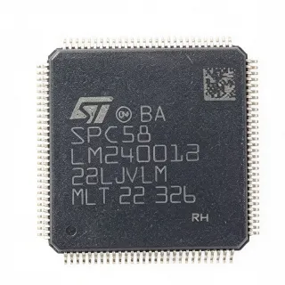
STM32F103ZEH6 - 72MHz Cortex-M3 512KB MCU | STMicroelectronics
Référence : STM32F103ZEH6 ✓ Actif| Qté | Prix unitaire | Total |
|---|---|---|
| 1 | $0 | $0,00 |
| 10 | $0 | $0,00 |
| 100 | $0 | $0,00 |
| 500 | $0 | $0,00 |
| 1 000 | $0 | $0,00 |
STM32F103ZEH6 Présentation
A microcontroller is a programmable system-on-chip that executes firmware, reads sensors, controls actuators, and manages digital interfaces. The STM32F103ZEH6 combines an ARM Cortex-M3 RISC core with Flash program memory, SRAM, direct-memory-access support, and multiple peripherals. Within the hierarchy, it is an embedded microcontroller, a 32-bit MCU, and a member of the STM32 family of ARM-based semiconductor devices.
Verified manufacturer information identifies a maximum CPU frequency of 72 MHz, 512 KB of Flash, USB, CAN, 11 timers, three ADCs, and 13 communication interfaces. Its broad peripheral mix allows several communications protocols and time-sensitive functions to coexist without external expansion devices. The high pin count also provides more externally accessible GPIO and peripheral connections than smaller STM32 packages.
The ARM Cortex-M3 core provides the instruction set and processing foundation, while the STM32 peripherals handle timers, analog conversion, serial communications, USB, and CAN. Multiple timers support periodic generation, input capture, encoder-related functions, and motor-control workflows. Three ADC channels groups permit analog measurements, while communication interfaces reduce demand for discrete protocol controllers.
Typical applications include industrial automation equipment, CAN-connected control panels, USB data loggers, communications hubs, motor controllers, and instrumentation gateways. The STM32F103ZEH6 is especially appropriate when firmware requires substantial Flash space and a broad set of embedded peripherals while retaining the established STM32F103 software ecosystem.
Designers should verify the complete pin assignment, power supply requirements, clock configuration, and peripheral multiplexing against the manufacturer datasheet before layout. A 144-pin LQFP package also demands careful escape routing and thermal-aware placement. Published pricing and stock conditions should be checked with authorized distributors because availability can change independently of technical suitability.
This page consolidates manufacturer specifications, distributor references, documented same-family alternatives, and practical procurement guidance. It also distinguishes verified data from unprovided parameters so engineers can assess fit without relying on assumptions.
Alternatives de remplacement direct pour STM32F103ZEH6 — même boîtier, compatible broche à broche. Les références à boîtier différent nécessitant une retouche du PCB sont exclues.
Variantes de cette série
Modèles de la même série directement compatibles avec STM32F103ZEH6 (même facteur de forme et même empreinte) — différant par Communication Interfaces, Package, Timers.
Outil de comparaison rapide — sélectionnez des références alternatives pour une comparaison côte à côte :
STM32F103ZEH7
✅ Remplacement direct📋 Alternative de référence (hors catalogue)
STM32F103ZEH7TR
✅ Remplacement direct📋 Alternative de référence (hors catalogue)
STM32F103ZET6
✅ Remplacement direct✓ En stock
$5.39 / unité
Voir la fiche technique →STM32F103ZDH6
✅ Remplacement direct📋 Alternative de référence (hors catalogue)
STM32F103ZEH6 Valeurs maximales et caractéristiques électriques
| Product Type | 32-bit ARM Cortex-M3 microcontroller |
| Maximum CPU Frequency | 72 MHz |
| Core Architecture | ARM Cortex-M3 32-bit RISC |
| Flash Memory | 512 KB |
| Flash Organization | 512K x 8 bits |
| Timers | 11 |
| ADC Channels | 3 |
| Communication Interfaces | 13 |
| USB Support | Yes |
| CAN Support | Yes |
| Performance | 1.25 DMIPS/MHz at 72 MHz |
| Package Pins | 144 pins |
| Boîtier | LQFP-144 |
| Type de montage | Surface mount |
| Product Line | STM32F1 performance line |
Guide de configuration des broches du STM32F103ZEH6 lqfp-144
Configuration des broches du STM32F103ZEH6 (boîtier lqfp-144). Ce circuit intégré numérique comprend des GPIO, des interfaces de communication (UART, SPI, I2C) et des broches d'alimentation. Consultez la fiche technique du fabricant pour les fonctions alternatives des broches et les options de configuration. Indispensable pour la conception de systèmes embarqués et la conception de circuits imprimés.

Aucune donnée de brochage détaillée disponible pour STM32F103ZEH6.
Consultez la fiche technique pour la configuration complète des broches.
Applications typiques
STM32F103ZEH6 convient pour 6 applications: Industrial Automation Controller, CAN-Connected Control Panel, USB Data Logger, Motor Control Subsystem, Communications Gateway, Instrumentation and Sensor Hub.
Industrial Automation Controller
The STM32F103ZEH6 fits industrial automation controllers because its 72 MHz Cortex-M3 core and 512 KB of Flash provide headroom for control loops, state machines, diagnostics, and communications. Eleven timers support periodic execution, input capture, and output comparison, while three ADC channels groups can process analog process variables. Use the USB and CAN connectivity for service access and distributed plant communication. The LQFP-144 package also exposes a broad pin set, but industrial deployments still require validated isolation, surge protection, grounding, and EMC design.
Recommandé
CAN-Connected Control Panel
STM32F103ZEH6 is appropriate for a CAN-connected control panel because the device combines a 72 MHz ARM Cortex-M3 core with built-in CAN, 11 timers, and 13 communication interfaces. Firmware can coordinate remote I/O, monitor operating states, and expose diagnostics while 512 KB of Flash accommodates application and protocol code. The 144-pin package provides ample signal access, but the physical layer still requires a transceiver, termination, common-mode protection, and controlled routing. A production design should validate bus timing under worst-case clock and interrupt loads.
Recommandé
USB Data Logger
The STM32F103ZEH6 suits a USB data logger that combines analog acquisition, local storage, configuration, and host communication. Its three ADC channels support sensor inputs, while 11 timers can schedule sampling, timestamp events, and drive indicators. The 512 KB of Flash provides more room for firmware than small STM32 variants, and 13 communication interfaces permit expansion. Firmware should use DMA thoughtfully to move samples without blocking control functions. USB power, ESD protection, clock stability, and ground-return planning must be validated at the board level.
Recommandé
Motor Control Subsystem
STM32F103ZEH6 can serve as the control MCU in a motor-control subsystem where a 72 MHz core, multiple timers, three ADC channels, and extensive communications are useful. Timers can generate deterministic control events, ADC channels can sample command or feedback signals, and CAN or serial links can coordinate with a larger machine. Firmware must verify timer channels, complementary outputs, break inputs, ADC trigger paths, and pin multiplexing in the exact LQFP-144 pinout. Current sensing, gate-driver timing, thermal protection, and overvoltage handling require dedicated validation.
Recommandé
Communications Gateway
The STM32F103ZEH6 is well matched to a communications gateway because 13 communication interfaces, USB, CAN, 512 KB of Flash, and a 72 MHz Cortex-M3 core allow several protocol layers to run concurrently. Firmware can bridge local fieldbus traffic to USB or another serial link while timers support periodic heartbeat and timeout functions. The broad LQFP-144 connection count reduces the need for additional I/O expanders. Real products must account for protocol timing, buffer depth, bus impedance, ESD, surge exposure, and secure update requirements.
Recommandé
Instrumentation and Sensor Hub
STM32F103ZEH6 can coordinate instrumentation and sensor-hub functions because three ADC channels, 11 timers, and 13 communication interfaces support concurrent measurement and control. The 512 KB Flash capacity is useful for calibration tables, drivers, protocol handlers, and diagnostic data. Engineers can use timer inputs for trigger capture and communication interfaces to aggregate remote sensors before forwarding results through USB or CAN. Calibration, reference accuracy, analog noise, grounding, and sampling timing must be verified in the target enclosure and operating environment.
Recommandé
Récapitulatif des produits recommandés
Données de référence d'ingénierie pour STM32F103ZEH6 — comparaison, recommandations de conception et informations de conformité.
Guide de sélection
Comparaison avec les alternatives
| Paramètre | Ce produit | STM32F103ZEH7 | STM32F103ZEH7TR | STM32F103ZET6 | STM32F103ZDH6 |
|---|---|---|---|---|---|
| Package | LQFP-144 | LQFP-144 | LQFP-144 | LQFP-144 | LQFP-144 |
| Brand | STMicroelectronics | STMicroelectronics | STMicroelectronics | STMicroelectronics | STMicroelectronics |
Principaux différenciateurs
- High verified Flash capacity within the STM32F103ZE orderable family (vs GD32F103ZET6)
- Broad integrated peripheral complement (vs STM32F103ZEH7)
- Same-family sourcing path (vs STM32F103ZET6)
Notes de conception
Treat the LQFP-144 footprint as a high-pin-count escape-routing problem. Assign pins by priority, keep sensitive analog and communication routes away from switching nodes, and route decoupling directly to the relevant supply pins with a low-impedance ground return. Confirm the manufacturer land pattern and pin-1 orientation before Gerber release; the supplied web results do not provide a verified pin table.
Build the supply network from the manufacturer's voltage and decoupling requirements rather than generic STM32 assumptions. The supplied data verifies a 72 MHz core and 512 KB Flash but does not provide operating-voltage limits or regulator recommendations. Confirm all VDD and VDDA pins, place bulk and high-frequency capacitance according to the datasheet, and measure startup droop under the highest expected peripheral load.
Do not substitute an STM32F103 family member solely because it has 144 pins. The supplied alternatives identify STM32F103ZEH7, STM32F103ZEH7TR, STM32F103ZET6, and STM32F103ZDH6 as related candidates, but their suffix-specific temperature, memory, qualification, and lifecycle details are not provided. Check the exact ordering code, compare every used peripheral and pin, rebuild the image, and run worst-case timing tests before approving a substitution.
Informations de conformité
The supplied records do not explicitly provide target-part RoHS, REACH, AEC-Q100, lead-free, halogen-free, or conflict-minerals declarations. Obtain current STMicroelectronics compliance documentation for the exact MPN.